

Page 1

/ Instruction Manual
Analog Input/Output Interface Card
"OPC-G1-AIO"
Fuji Electric Co., Ltd. INR-SI47-1288b-JE
Page 2

English Version
Page 3

Page 4
Preface
Thank you for purchasing our analog input/output interface card.
This instruction manual describes the analog input/output interface card "OPC-G1-AIO" designed for the
FRENIC-MEGA series of inverters.
Mounting the analog input/output interface card on your FRENIC-MEGA enables analog input (voltage and
current for each terminal) and analog output (voltage and current for each terminal) to/from the inverter.
The analog input/output interface card can be connected to any one of the three option connection ports (A-, B-,
and C-ports) on the FRENIC-MEGA.
This instruction manual does not contain inverter handling instructions. Read through this instruction manual in
conjunction with the FRENIC-MEGA Instruction Manual and be familiar with proper handling and operation of
this product. Improper handling might result in incorrect operation, a short life, or even a failure of this product.
Keep this manual in a safe place.
• Read through this instruction manual and be familiar with the analog input/output interface card before
proceeding with installation, connections (wiring), operation, or maintenance and inspection.
• Improper handling might result in incorrect operation, a short life, or even a failure of this product as
well as the motor.
• Deliver this manual to the end user of this product. Keep this manual in a safe place until this product
is discarded.
Safety precautions
Read this manual thoroughly before proceeding with installation, connections (wiring), operation, or
maintenance and inspection. Ensure you have sound knowledge of the device and familiarize yourself with all
safety information and precautions before proceeding to operate the inverter.
Safety precautions are classified into the following two categories in this manual.
Failure to heed the information indicated by this symbol may lead to
dangerous conditions, possibly resulting in death or serious bodily injuries.
Failure to heed the information indicated by this symbol may lead to
dangerous conditions, possibly resulting in minor or light bodily injuries
and/or substantial property damage.
Failure to heed the information contained under the CAUTION title can also result in serious consequences.
These safety precautions are of utmost importance and must be observed at all times.
i
Page 5
Installation and wiring
• Before starting installation and wiring, turn OFF the power and wait at least five minutes for inverters
with a capacity of 22 kW or below, or at least ten minutes for inverters with a capacity of 30 kW or
above. Make sure that the LED monitor and charging lamp are turned OFF. Further, make sure,
using a multimeter or a similar instrument, that the DC link bus voltage between the terminals P(+)
and N(-) has dropped to the safe level (+25 VDC or below).
• Qualified electricians should carry out wiring.
Otherwise, an electric shock could occur.
• Do not use the product that is damaged or lacking parts.
Doing so could cause a fire, an accident, or injuries.
• Prevent lint, paper fibers, sawdust, dust, metallic chips, or other foreign materials from getting into
the inverter and the option.
Otherwise, a fire or an accident might result.
• Incorrect handling in installation/removal jobs could cause a failure.
A failure might result.
• Noise may be emitted from the inverter, motor and wires. Implement appropriate measure to prevent
the nearby sensors and devices from malfunctioning due to such noise.
Otherwise, an accident could occur.
Operation
• Be sure to install the front cover before turning the inverter's power ON. Do not remove the cover
when the inverter power is ON.
Otherwise, an electric shock could occur.
• Do not operate switches with wet hands.
Doing so could cause an electric shock.
• If you configure the function codes wrongly or without completely understanding FRENIC-MEGA
Instruction Manual and the FRENIC-MEGA User's Manual, the motor may rotate with a torque or at a
speed not permitted for the machine. Confirm and adjust the setting of the function codes before
running the inverter.
Otherwise, an accident could occur.
Maintenance and inspection, and parts replacement
• Before proceeding to the maintenance/inspection jobs, turn OFF the power and wait at least five
minutes for inverters with a capacity of 22 kW or below, or at least ten minutes for inverters with a
capacity of 30 kW or above. Make sure that the LED monitor and charging lamp are turned OFF.
Further, make sure, using a multimeter or a similar instrument, that the DC link bus voltage between
the terminals P(+) and N(-) has dropped to the safe level (+25 VDC or below).
Otherwise, an electric shock could occur.
• Maintenance, inspection, and parts replacement should be made only by qualified persons.
• Take off the watch, rings and other metallic objects before starting work.
• Use insulated tools.
Otherwise, an electric shock or injuries could occur.
ii
Page 6

Disposal
• Treat the interface card as an industrial waste when disposing of it.
Otherwise injuries could occur.
Others
• Never modify the interface card.
Doing so could cause an electric shock or injuries.
Icons
The following icons are used throughout this manual.
This icon indicates information which, if not heeded, can result in the product not operating to full
efficiency, as well as information concerning incorrect operations and settings which can result in
accidents.
This icon indicates information that can prove handy when performing certain settings or operations.
This icon indicates a reference to more detailed information.
iii
Page 7

Table of Contents
Preface ............................................................................... i
Safety precautions ............................................................. i
Chapter 1 BEFORE USING THIS OPTION ..................... 1-1
1.1 Acceptance Inspection ........................................... 1-1
1.2 Applicable Inverters ................................................ 1-2
1.3 Operating Environment .......................................... 1-2
1.4 Installation and Removal of the Interface Card .......1-2
1.4.1 Installing the interface card ............................ 1-3
1.4.2 Removing the interface card .......................... 1-4
1.5 Wiring ..................................................................... 1-5
1.6 Terminal Allocation and Symbol Diagram ............... 1-7
Chapter 2 WIRING .......................................................... 2-1
2.1 Connection Diagram ................................................. 2-1
2.2 Terminal Functions ................................................... 2-2
2.3 Configuring Inverter's Function Codes ..................... 2-4
2.4 Function Codes Details ............................................ 2-6
Chapter 3 I/O CHECKING ............................................... 3-1
Chapter 4 PROTECTIVE FUNCTION ............................. 4-1
iv
Page 8
Chapter 1 BEFORE USING THIS OPTION
1.1 Acceptance Inspection
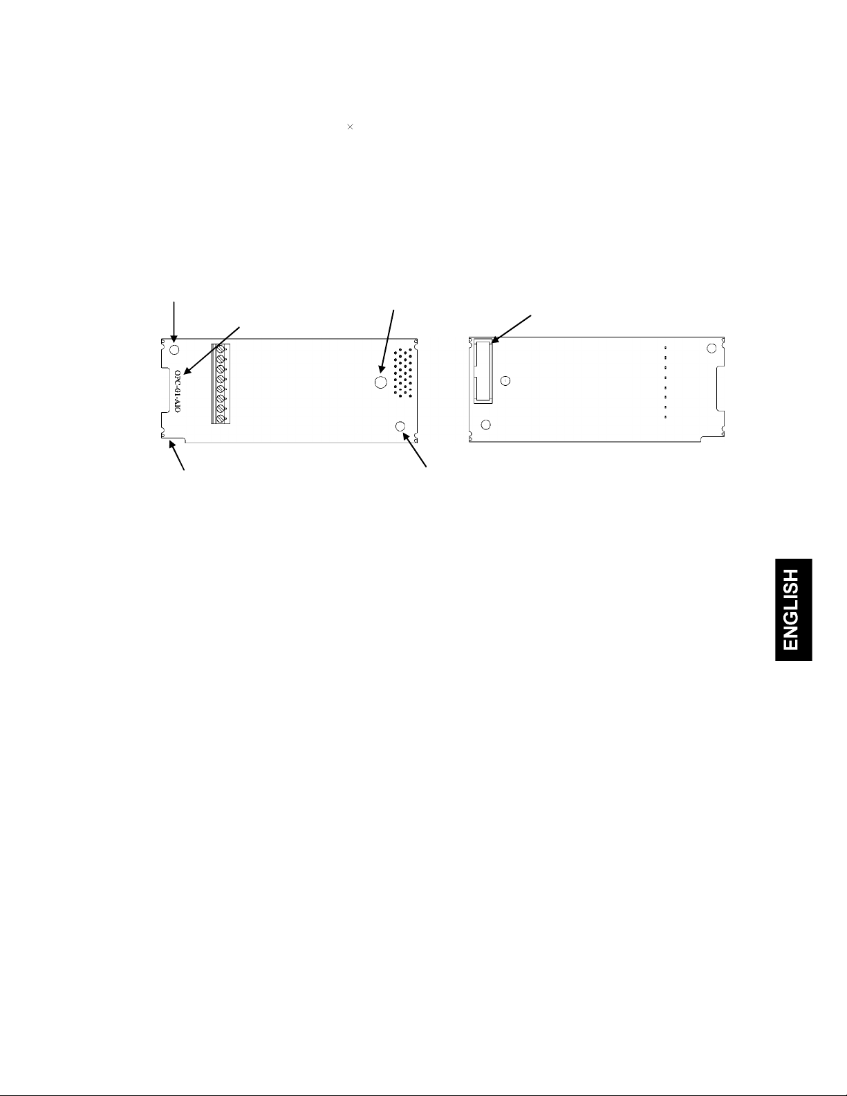
Unpack the package and check the following:
(1) An interface card, two screws (M3 8), and the Analog Input/Output Interface Card Instruction Manual (this
manual) are contained in the package.
(2) The interface card is not damaged during transportation--no defective parts, dents or warps.
(3) The model name "OPC-G1-AIO" is printed on the interface card. (See Figure 1.1.)
If you suspect the product is not working properly or if you have any questions about your product, contact the
shop where you bought the product or your local Fuji branch office.
Screw hole (left)
Model name
(Front) (Back)
Positioning cutout
Figure 1.1 Name of Parts on Analog Input/Output Interface Card (OPC-G1-AIO)
Release knob
Screw hole (right)
CN1
1-1
Page 9
1.2 Applicable Inverters
This interface card is applicable to the following inverters and ROM version.
Table 1.1 Applicable inverter and ROM version
Series Inverter type Applicable motor rating ROM version
FRENIC-MEGA FRN G1 - All capacities 0700 or later
* The boxes replace alphabetic letters depending on the nominal applied motor, enclosure, and power supply voltage.
To check the inverter's ROM version, use Menu #5 "Maintenance Information" on the keypad. (Refer to the
FRENIC-MEGA Instruction Manual, Chapter 3, Section 3.4.6 "Reading maintenance information."
Display on LED Monitor Item Description
Inverter's ROM version Shows the inverter's ROM version as a 4-digit code.
1.3 Operating Environment
Install the inverter equipped with this interface card in an environment that satisfies the requirements listed in
Table 1.2.
Table 1.2 Environmental Requirements
Item Specifications
Site location Indoors
Surrounding temperature
Relative humidity 5 to 95% (No condensation)
Atmosphere
Altitude 1,000 m max.
Atmospheric pressure 86 to 106 kPa
Vibration Refer to the FRENIC-MEGA Instruction Manual, Chapter 2.
(Note) Do not install the inverter in an environment where it may be exposed to lint, cotton waste or moist dust or dirt which will
clog the heat sink of the inverter. If the inverter is to be used in such an environment, install it in a dustproof panel of your
system.
Refer to the FRENIC-MEGA Instruction Manual, Chapter 2.
The inverter must not be exposed to dust, direct sunlight, corrosive gases, flammable
gases, oil mist, vapor or water drops.
Pollution degree 2 (IEC60664-1) (Note)
The atmosphere can contain a small amount of salt.
(0.01 mg/cm2 or less per year)
The inverter must not be subjected to sudden changes in temperature that will
cause condensation to form.
1.4 Installation and Removal of the Interface Card
Before starting installation and wiring, turn OFF the power and wait at least five minutes for inverters with a
capacity of 22 kW or below, or at least ten minutes for inverters with a capacity of 30 kW or above. Make
sure that the LED monitor and charging lamp are turned OFF. Further, make sure, using a multimeter or a
similar instrument, that the DC link bus voltage between the terminals P(+) and N(-) has dropped to the safe
level (+25 VDC or below).
Otherwise, an electric shock could occur.
1-2
Page 10

• Do not use the product that is damaged or lacking parts.
Doing so could cause a fire, an accident, or injuries.
• Prevent lint, paper fibers, sawdust, dust, metallic chips, or other foreign materials from getting into
the inverter and the interface card.
Otherwise, a fire or an accident might result.
• Incorrect handling in installation/removal jobs could cause a failure.
A failure might result.
1.4.1 Installing the interface card
Before mounting the interface card, perform the wiring for the main circuit terminals and control circuit
terminals.
(1) Remove the front cover from the inverter and expose the control printed circuit board (control PCB). As
shown in Figure 1.2, the interface card can be connected to any one of the three option connection ports
(A-, B-, and C-ports) of the inverter.
To remove the front cover, refer to the FRENIC-MEGA Instruction Manual, Section 2.3. For inverters
with a capacity of 30 kW or above, open also the keypad enclosure.
(2) Insert connector CN1 on the back of the interface card (Figure 1.1) into any of the A-port (CN4), B-port
(CN5), and C-port (CN6) on the inverter's control PCB. Then tighten the two screws that come with the card.
(Figure 1.4)
Check that the positioning cutout (shown in Figure 1.1) is fitted on the tab ( in Figure 1.3) and
connector CN1 is fully inserted ( in Figure 1.3). Figure 1.4 shows the interface card correctly
mounted.
(3) Perform wiring on the interface card.
Refer to Section 1.5 "Wiring."
(4) Put the front cover back into place.
To put back the front cover, refer to the FRENIC-MEGA Instruction Manual, Section 2.3. For inverters
with a capacity of 30 kW or above, close also the keypad enclosure.
Figure 1.2 In the case of 0.4 kW
1-3
Page 11

Fit the positioning cutout of the card over the
tab on the inverter to determine the mounting
position.
Insert connector CN1 on the card into any of
the three ports (A-, B- and C-ports) on the
inverter's control PCB.
Note: Be sure to follow the order of and .
Inserting CN1 first may lead to
insufficient insertion, resulting in a
contact failure.
Tab
Figure 1.3 Mounting the Interface Card (to B-port)
(Release knob)
Figure 1.4 Mounting Completed (on B-port)
1.4.2 Removing the interface card
Remove the two screws that secure the interface card and pull the release knob (shown above) to take the card
out of the inverter.
1-4
Page 12

1.5 Wiring
• Before starting installation and wiring, turn OFF the power and wait at least five minutes for inverters with
a capacity of 22 kW or below, or at least ten minutes for inverters with a capacity of 30 kW or above.
Make sure that the LED monitor and charging lamp are turned OFF. Further, make sure, using a
multimeter or a similar instrument, that the DC link bus voltage between the terminals P(+) and N(-) has
dropped to the safe level (+25 VDC or below).
• Qualified electricians should carry out wiring.
Otherwise, an electric shock could occur.
• In general, the covers of the control signal wires are not specifically designed to withstand a high voltage
(i.e., reinforced insulation is not applied). Therefore, if a control signal wire comes into direct contact with
a live conductor of the main circuit, the insulation of the cover might break down, which would expose the
signal wire to a high voltage of the main circuit. Make sure that the control signal wires will not come into
contact with live conductors of the main circuit.
Failure to observe this precaution could cause an electric shock or an accident.
Noise may be emitted from the inverter, motor and wires.
Take appropriate measures to prevent the nearby sensors and devices from malfunctioning due to such
noise.
An accident could occur.
Perform wiring for the interface card observing the precautions below. Refer to the connection diagram shown in
Figure 2.1 (Chapter 2) and the wiring examples shown in Figure 1.7.
(1) Turn the inverter's power OFF.
(2) Use shielded wires.
(3) To prevent malfunction due to noise, keep the wiring for the interface card away from the main circuit wiring
and other power lines as far as possible. Never install them in the same wire duct.
(4) Complete wiring before turning the inverter ON.
(5) See Table 1.3 for the specifications of the terminal block on the interface card.
When using stripped wires (without attaching a crimp terminal), strip the wire end by 5 to 7 mm. (Figure 1.5)
When using a crimp terminal, attach a vinyl-insulated ferrule.
Loosen the terminal screw, insert the wire end into above the metal part of the terminal block, and tighten
the screw to fasten it. (Figure 1.6)
Table 1.3 Terminal Specifications
Item Specifications
Wire size
Terminal screw size M2
Tightening torque 0.22 to 0.25 N·m
5 to 7 mm
AWG24 to AWG18 (0.25 to 0.75 mm2),
wire with rated temperature 105°C (UL) recommended
Figure 1.5 Wire End Treatment (For Connection to
Terminals on Interface Card)
Figure 1.6 Connecting to a Terminal
on Interface Card
• Route the wiring of the interface circuit terminals as far from the wiring of the main circuit as
possible. Otherwise electric noise may cause malfunctions.
• Fix the interface circuit wires with a cable tie inside the inverter to keep them away from the live
parts of the main circuit (such as the terminal block of the main circuit).
1-5
Page 13

Depending upon the wire type and the number of wires used, the front cover may be lifted by the
wires, which impedes normal keypad operation. If it happens, change the wire type or size.
Route the wires, taking care not to let them go over the control PCB, as shown in Figure 1.7.
Otherwise, malfunctions may occur.
• For inverters with a capacity of 22 kW or below
When grounding the shielded cable, use a
crimp ring terminal with insulation sheath,
R1.25-3 or the like and fasten it together
with the card using this screw.
Location for grounding
the shielded cable
* Pass the wires from the interface card between the control
circuit terminal block and the front cover.
In the case of 0.4 kW
• For inverters with a capacity of 30 kW or above
In the case of 75 kW
Figure 1.7 Examples of Wiring
1-6
Page 14

1.6 Terminal Allocation on the Interface Card
CS+ CS- Ao+ Ao- C2 P10 32 31
Figure 1.8 Terminal Allocation and Symbol Diagram
1-7
Page 15

Chapter 2 WIRING
A
A
2.1 Connection Diagram
FRENIC-MEGA
Power supply for
the potentiometer
Analog voltage
input
0 to +10 VDC
(0 to ±10 VDC)
Analog current
input
4 to 20 mA DC
L1/R
L2/S
L3/T
U
V
W
OPC-G1-AIO
3
2
1
(+)
(-)
P10
Analog current
output
4 to 20 mA DC
+10 VDC
32
31
C2
Analog voltage
output
0 to ±10 VDC
+24 VDC
0 V
o+
o-
Analog voltmeter
CS+
CS-
Analog ammeter
Figure 2.1 Connection Diagram
2-1
Page 16

2.2 Terminal Functions
Symbol Name Functions
Table 2.1 Terminals and Their Specifications
P10 Power supply
for the
potentiometer
32 Analog
voltage input
C2 Analog
current input
31 Analog
common
Ao+ Analog
voltage output
(+)
Power supply for frequency command potentiometer (Variable resistor: 1 to 5 k )
The potentiometer of 1/2 W rating or more should be connected.
(10 VDC, 10 mA DC max.)
(1) Used as analog voltage input from external equipment. One of the following
signals can be assigned to this terminal by specifying o60 data.
- Auxiliary frequency command - PID command
- PID feedback amount - Ratio setting
- Torque limiter level - Analog input monitor
(2) Hardware specifications
• Input voltage: 0 to 10 VDC/0 to 100% (0 to 5 VDC/0 to 100%)
• Input impedance: 22 k
• The maximum input is 15 VDC, however, the voltage higher than 10
VDC is handled as 10 VDC.
• Resolution: 1/3000
• Adjustable range of the gain: 0.00 to 200%
(1) Used as analog current input from external equipment. One of the following
signals can be assigned to this terminal by specifying o66 data.
- Auxiliary frequency command - PID command
- PID feedback amount - Ratio setting
- Torque limiter level - Analog input monitor
(2) Hardware specifications
• Input current: 4 to 20 mA DC/0 to 100%
• Input impedance: 250
• The maximum input is +30 mA DC, however, the current larger than
+20 mA DC is handled as +20 mA DC.
• Resolution: 1/3000
• Adjustable range of the gain: 0.00 to 200%
Reference terminal for [P10], [32] and [C2].
Isolated from terminals [CS+] and [CS-].
Same potential as terminals [Ao-] and [11] on the inverter.
(1) Outputs the monitor signal of analog DC voltage (0 to 10 VDC). One of the
following signals can be issued from this terminal by specifying o71 data.
- Output frequency - Output current - Output voltage
- Output torque - Load factor - Input power
- PID feedback amount - PG feedback value
- DC link bus voltage - Universal AO
- Motor output - Calibration
- PID command (SV) - PID output (MV)
Ao- Analog
voltage output
(-)
(2) Hardware specifications
• Output voltage: 0 to 10 VDC
• Input impedance of the external device: Min. 5 k (at 0 to 10 VDC
output)
(While the terminal is outputting 0 to 10 VDC, it is capable of driving
up to two analog voltmeters with 10 k impedance.)
• Resolution: 1/3000
• Adjustable range of the gain: 0 to 300%
Reference terminal for [Ao+].
Isolated from terminals [CS+] and [CS-].
Same potential as terminal [31] and [11] on the inverter.
2-2
Page 17

Symbol Name
C
Functions
CS+ Analog
current
output (+)
(1) Outputs the monitor signal of analog DC current (4 to 20 mA DC). One of the
following signals can be issued from this terminal by specifying o74 data.
- Output frequency - Output current - Output voltage
- Output torque - Load factor - Input power
- PID feedback amount - PG feedback value
- DC link bus voltage - Universal AO
- Motor output - Calibration
- PID command (SV) - PID output (MV)
(2) Hardware specifications
• Output current: 4 to 20 mA DC
• Input impedance of the external device: Max. 500 (at 4 to 20 mA DC
output)
• Resolution: 1/3000
• Adjustable range of the gain: 0 to 300%
<Control circuit>
Current
Ammeter
24 VDC
urrent
source
CS+
CS-
CS- Analog
current
output (-)
CM
([CM] on the inverter)
2-3
Page 18

2.3 Configuring Inverter's Function Codes
Table 2.2 lists the function codes related to the analog input/output interface card.
Function codes o66 through o75 become available when the interface card is connected to the inverter.
Table 2.2 Function Codes and Parameters
Drive control *3
Function
code
o60
o61
o62
o63
o64
o65
o66
o67
Name Data setting range
Terminal [32] Function
(Mode selection)
(Offset adjustment) -5.0 to +5.0%
(Gain adjustment) 0.00 to 200.00%
(Filter setting) 0.00 to 5.00 s
(Gain base point) 0.00 to 100.00%
(Polarity) 0: Bipolar
Terminal [C2] Function
(Mode selection)
(Offset adjustment) -5.0 to +5.0%
0: No assignment
1: Auxiliary frequency command 1
2: Auxiliary frequency command 2
3: PID command
5: PID feedback amount
6: Ratio setting
7: Analog torque limit value A
8: Analog torque limit value B
20: Analog input monitor
1: Unipolar
0: No assignment
1: Auxiliary frequency command 1
2: Auxiliary frequency command 2
3: PID command
5: PID feedback amount
6: Ratio setting
7: Analog torque limit value A
8: Analog torque limit value B
20: Analog input monitor
w/o
PG
w/
PG
V/f
N Y 0 Y Y Y
Y* Y 0.0 Y Y Y
Y* Y 100.00 Y Y Y
Y Y 0.05 Y Y Y
Y* Y 100.00 Y Y Y
N Y 1 Y Y Y
N Y 0 Y Y Y
Y* Y 0.0 Y Y Y
o68
o69
o70
*1 Y*: Possible, Y: Possible, N: Impossible
(For details about Y* and Y, refer to the FRENIC-MEGA Instruction Manual, Chapter 5, Section 5.1 "Function Code
Tables.")
*2 Y: Possible, N: Impossible
*3 Y: Applicable, N: Not applicable
(Gain adjustment) 0.00 to 200.00%
(Filter setting) 0.00 to 5.00 s
(Gain base point) 0.00 to 100.00%
2-4
Y* Y 100.00 Y Y Y
Y Y 0.05 Y Y Y
Y* Y 100.00 Y Y Y
Page 19

Drive control *3
Function
code
o71
o72
Name Data setting range
Terminal [Ao] Function
(Mode selection)
(Gain to output voltage) 0 to 300%
0: Output frequency 1
(before slip compensation)
1: Output frequency 2
(after slip compensation)
2: Output current
3: Output voltage
4: Output torque
5: Load factor
6: Input power
7: PID feedback amount
8: PG feedback value (speed)
9: DC link bus voltage
10: Universal AO
13: Motor output
14: Calibration
15: PID command (SV)
16: PID output (MV)
w/o
PG
w/
PG
V/f
Y Y 0 Y Y Y
Y* Y 100 Y Y Y
o73
o74
o75 (Gain to output current) 0 to 300% Y* Y 100
*1 Y*: Possible, Y: Possible, N: Impossible
(For details about Y* and Y, refer to the FRENIC-MEGA Instruction Manual, Chapter 5, Section 5.1 "Function Code
Tables.")
*2 Y: Possible, N: Impossible
*3 Y: Applicable, N: Not applicable
Terminal [CS] Function
(Polarity) 0: Bipolar
(Mode selection)
1: Unipolar
0: Output frequency 1
(before slip compensation)
1: Output frequency 2
(after slip compensation)
2: Output current
3: Output voltage
4: Output torque
5: Load factor
6: Input power
7: PID feedback amount
8: PG feedback value (speed)
9: DC link bus voltage
10: Universal AO
13: Motor output
14: Calibration
15: PID command (SV)
16: PID output (MV)
Y Y 1 Y Y Y
Y Y 0 Y Y Y
Y Y Y
2-5
Page 20

2.4 Function Codes Details
This section details the function codes.
AI function (o60 and o66)
Configure function codes o60 and o66 to assign functions to terminals [32] and [C2].
o60 o66 Function Description
0 0 No assignment
1 1 Auxiliary frequency command 1
2 2 Auxiliary frequency command 2
3 3 PID command
5 5 PID feedback amount
6 6
7 7 Analog torque limit value A
8 8 Analog torque limit value B
Ratio setting
The analog input function is disabled by default.
0 to 10 V/0 to 100%
4 to 20 mA/0 to +100%
• 100% = Maximum frequency
• Positive during forward rotation
• Negative during reverse rotation
0 to 10 V/0 to 100%
4 to 20 mA/0 to +100%
• Under PID process control: Unipolar
• Under dancer reference position control: Bipolar
• 100% = 100% of the PID command
0 to 10 V/0 to 100%
4 to 20 mA/0 to +100%
• 100% = 100% of the PID feedback amount
0 to +10 V/0 to +100%
4 to 20 mA/0 to +100%
• +100% = Ratio 1
0 to 10 V/0 to 100%
4 to 20 mA/0 to +100%
• 100% = 200% of the rated motor torque
20 20 Analog input monitor
0 to +10 V/
Display coefficient B (E41) to display coefficient A (E42)
4 to 20 mA/
Display coefficient B (E41) to display coefficient A (E42)
2-6
Page 21

Gain (o62, o64, o68 and o70)
Specified value
100%
Gain
(o62, o68)
0
Point
X
Gain base
point
(o64, o70)
Analog input
100%
Filter (o63 and o69)
o63 and o69 configure a filter time constant for an analog voltage and current input, respectively. The larger the
time constant, the slower the response. Specify the proper filter time constant taking into account the response
speed of the machine (load).
- Data setting range: 0.00 to 5.00 (s)
Polarity (o65)
o65 configures the input range for analog input voltage.
o65 Specifications for terminal input
0 -10 to +10 V
1 0 to +10 V (A negative component of the input will be regarded as 0 VDC.)
2-7
Page 22

AO function (o71 and o74)
Configure function codes o71 and o74 to assign functions to terminals [Ao] and [CS].
o71 o74 Function Description
0 0
1 1
2 2
3 3
4 4
5 5
6 6
7 7
8 8
9 9
10 10
11 11
13 13
14 14
15 15
Output frequency 1
(before slip compensation)
Output frequency 2
(after slip compensation)
Output current
Output voltage
Output torque
Load factor
Input power
PID feedback amount
PG feedback value (speed)
DC link bus voltage
Universal AO
Motor output
Calibration Outputs 10 V or 20 mA.
PID command (SV)
PID output (MV)
0 to 10 V/0 to 100%
4 to 20 mA/0 to +100%
• 100% = Maximum frequency
0 to 10 V/0 to 200%
4 to 20 mA/0 to +200%
• 100% = Inverter rated current
200 V class series:
0 to +10 V/0 to +250 V
4 to 20 mA/0 to +250 V
400 V class series:
0 to + 10 V/0 to +500 V
4 to 20 mA/0 to +500 V
0 to 10 V/0 to 200%
4 to 20 mA/0 to +200%
• 100% = Motor rated torque
0 to +10 V/0 to +200%
4 to 20 mA/0 to +200%
• 100% = Motor rated load
0 to +10 V/0 to +200%
4 to 20 mA/0 to +200%
• 100% = Inverter rated output
0 to +10 V/0 to +100%
4 to 20 mA/0 to +100%
• 100% = 100% of the PID feedback amount
0 to 10 V/0 to 100%
4 to 20 mA/0 to +100%
• 100% = Maximum frequency
200 V class series:
0 to +10 V/0 to +500 V
4 to 20 mA/0 to +500 V
400 V class series:
0 to +10 V/0 to +1000 V
4 to 20 mA/0 to +1000 V
0 to 10 V/0 to 100%
4 to 20 mA/0 to +100
• 100% = 20000d
0 to 10 V/0 to 200%
4 to 20 mA/0 to +200%
• 100% = Motor rated output
0 to 10 V/0 to 100%
• 100% = Feedback amount
0 to 10 V/0 to 100%
• 100% = Maximum frequency
2-8
Page 23

Gain (o72 and o75)
F30 = 300%
F30 = 200%
10 V
5 V
0 V
0%
50%33%
Meter scale
Polarity (o73)
o73 configures the output range for analog output voltage.
o73 Specifications for terminal input
0 -10 to +10 V
1 0 to +10 V (A negative component reverses the output.
Example: -5V +5V)
F30 = 100%
F30 = 50%
100%
2-9
Page 24

Chapter 3 I/O CHECKING
Using Menu #4 "I/O Checking" in FRENIC-MEGA program mode displays the I/O status of external signals on
the LED monitor of the keypad.
Figure 3.1 Menu Transition in Menu #4 "I/O Checking"
Basic key operation
To check the status of the I/O signals, set function code E52 to "2" (Full-menu mode) beforehand.
(1) Turn the inverter ON. It automatically enters Running mode. In that mode, press the key to switch to
Programming mode. The function selection menu appears.
(2) Use the and keys to display "I/O Checking" ( ).
(3) Press the key to proceed to a list of I/O check items (e.g. ).
(4) Use the and keys to display the desired I/O check item, then press the key.
The corresponding I/O check data appears.
(5) Press the key to return to the list of I/O check items. Press the key again to return to the menu.
For details of Menu #4 "I/O Checking," refer to the FRENIC-MEGA Instruction Manual, Chapter 3, Section
3.4 "Programming Mode."
3-1
Page 25

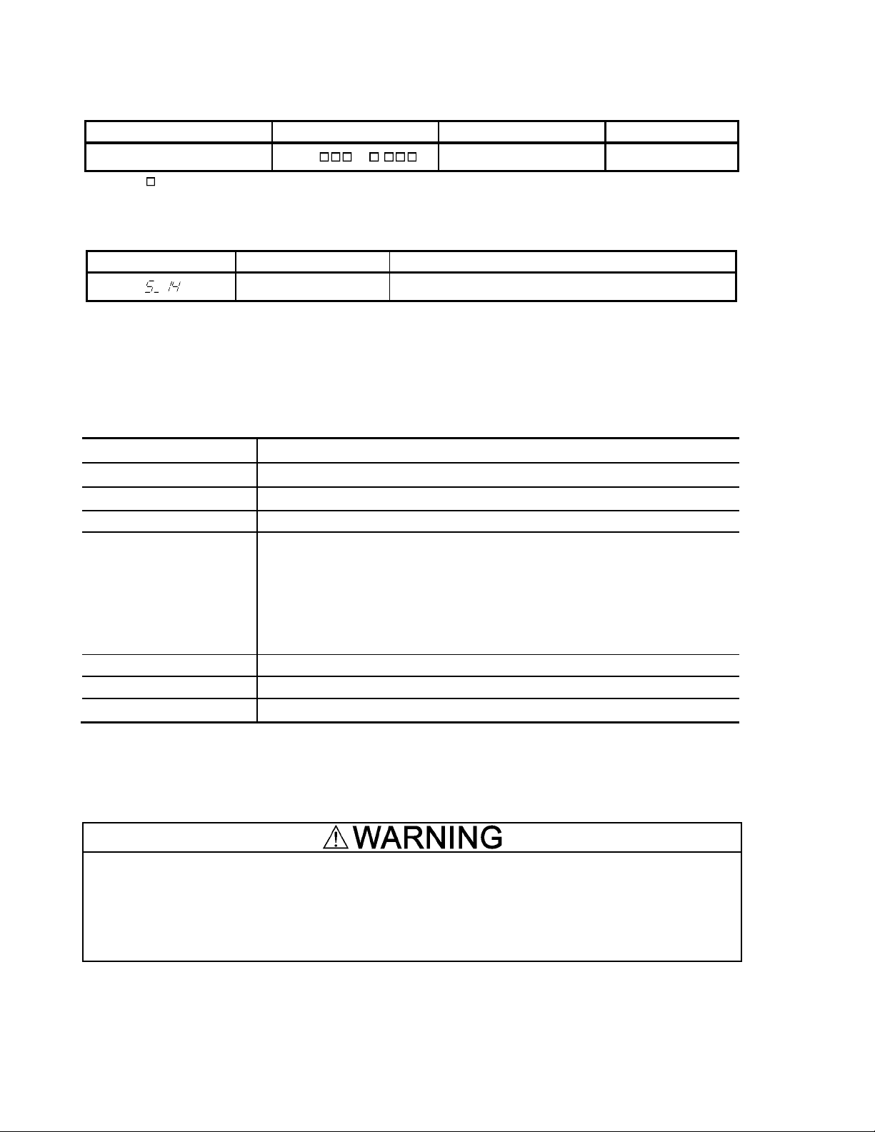
Table 3.1 I/O Check Items
LED monitor
shows:
Item Description
Input voltage on terminal [32] Shows the input voltage on terminal [32] in volts (V).
Input current on terminal [C2] Shows the input current on terminal [C2] in milliamperes (mA).
Output voltage on terminal [Ao] Shows the output voltage on terminal [Ao] in volts (V).
Output current on terminal [CS] Shows the output current on terminal [CS] in milliamperes (mA).
3-2
Page 26

Chapter 4 PROTECTIVE FUNCTION
Option communications error ( )
Problem A communications error occurred between the analog input/output interface card and the inverter.
Possible Causes What to Check and Suggested Measures
(1) There is a problem with the
connection between the
interface card and the
inverter.
(2) Strong electrical noise.
(3) Two or more interface cards
of the same type are
mounted.
Check whether the connector on the interface card is firmly engaged with that of
the inverter.
Reload the interface card into the inverter.
Check whether appropriate noise control measures have been implemented (e.g.
correct grounding and routing of signal wires, communications cables, and main
circuit wires).
Implement noise control measures.
Check whether two or more interface cards of the same type are mounted.
Limit the number of interface cards of the same type on an inverter to only
one.
When no o code is displayed even if an interface card is mounted, check whether the connector on
the interface card is firmly engaged with that of the inverter. In this case, does not appear.
Option error ( )
Problem An error occurred on the analog input/output interface card.
Possible Causes What to Check and Suggested Measures
(1) An error occurred on the
interface card mounted on the
inverter.
Check whether this error is due to the interface card itself.
The CPU or its printed circuit board (PCB) is defective. Contact your Fuji
Electric representative.
4-1
Page 27

Page 28

Analog Input/Output Interface Card
"OPC-G1-AIO"
Instruction Manual
First Edition, April 2008
Third Edition, April 2011
Fuji Electric Co., Ltd.
The purpose of this manual is to provide accurate information in the handling, setting up and operating of
the analog input/output interface card for the FRENIC-MEGA series of inverters. Please feel free to send
your comments regarding any errors or omissions you may have found, or any suggestions you may have
for generally improving the manual.
In no event will Fuji Electric Co., Ltd. be liable for any direct or indirect damages resulting from the
application of the information in this manual.
Page 29

URL http://www.fujielectric.co.jp/
Fuji Electric Co., Ltd.
Gate City Ohsaki, East Tower, 11-2, Osaki 1-chome,
Shinagawa-ku, Tokyo, 141-0032, Japan
Phone: +81 3 5435 7283 Fax: +81 3 5435 7425
URL http://www.fujielectric.com/
2011-04 (D11b/L08) 1CM
 Loading...