

Page 1

Victoreen® 875
June 2008
Manual No. 877-1-1 Rev. 11
©2004, 2005, 2008, 2009 Fluke Corporation, All rights reserved. Pri
All product names are trademarks of their respective companies
High Range Containment Monitor
Operators Manual
nted in U.S.A.
Page 2

Page 3

Fluke Biomedical
6045 Cochran Road
Cleveland, Ohio 44139
440.498.2564
www.flukebiomedical.com
Page 4

Table of Contents
SECTION 1:
1.1 G
1.2 Specifications......................................................................................................................... 1-1
1.3 Equipment Overview..............................................................................................................1-3
.4 Receiving Inspection.............................................................................................................. 1-8 1
.5 Storage................................................................................................................................... 1-9
1
1.6 Procedures, Warnings, and Cautions....................................................................................1-9
INTRODUCTION ......................................................................................... 1-1
eneral Description ............................................................................................................... 1-1
SECTION 2: INSTALLATION .......................................................................................... 2-1
2.1 Installation.............................................................................................................................. 2-1
2.2 Cable and Wiring Installation................................................................................................. 2-3
SECTION 3: OPERATION ............................................................................................... 3-1
3.1 Operation ............................................................................................................................... 3-1
SECTION 4: FUNCTIONAL DESCRIPTION.................................................................... 4-1
4.1 Functional Description ........................................................................................................... 4-1
4.2 Readout Module 876A-1........................................................................................................ 4-1
SECTION 5: MAINTENANCE, CALIBRATION, AND TROUBLESHOOTING................. 5-1
5.1 Maintenance........................................................................................................................... 5-1
5.2 Field Calibration..................................................................................................................... 5-1
5.3 Troubleshooting ..................................................................................................................... 5-3
5.4 Power Supply Measurements................................................................................................ 5-4
5.5 Signal Input Circuit................................................................................................................. 5-4
5.6 Metering Circuit...................................................................................................................... 5-5
5.7 The Alarm Circuits.................................................................................................................. 5-5
5.8 High Alarm Circuit.................................................................................................................. 5-6
5.9 Muting Stages of the Alarm Circuits....................................................................................... 5-6
5.10 ESC Board............................................................................................................................. 5-7
5.11 Overall Fail Circuitry Associated with the ECS Test.............................................................. 5-9
5.12 Starting with Pins M and P on the Power Supply Schematic ................................................ 5-9
5.13 Starting with Terminal H on Relay Driver Board.................................................................... 5-9
5.14 Provision of Inputs to Terminals M and P on the Power Supply Board................................. 5-9
5.15 Outputs of U206 Pulse Generator on the ECS Board ......................................................... 5-10
5.16 Operation of the Latch Circuit.............................................................................................. 5-10
i
Page 5

APPENDIX A
A.1 Calibration Procedures ..........................................................................................................A-1
A.2 Test Procedures............................................................................................................ .........A-1
APPENDIX B
B.1 Cable and Pull Box Procedures.................................................. -1
...........................................B
PPENDIX C
A
C.1 Applicable Drawings........................................................................................................
C.2 Bill of Materials...........
............................................................................................................C-3
.......C-1
ii
Page 6

General Information
General Description
1
Section 1
Introduction
1.1 General Desc
Containment Monitor 8
Containment Monitor 875 functions as an accident monitor for reactor containments
sists of the 877-1 Ion Chamber Detector that is located within the reactor containment, and the 876A-
con
1 Readout Module that is con
supply that provides the nece
onnected to the detector by two cables, a coaxial high voltage cable and a coaxial signal cable.
c
Specific le are contained b
1
Detector 877-1
Radiation Detected Photons above 60 keV
ations for the detector and readout modu elow.
.2 Specifications
ription
75
NOTE
The 875 Containment Monitor has been qualified
for use in Nuclear Safety related applications.
Qualification Test Rep
950.310A define the
verified by test and ar le for purchase.
tained in a rack in the control room. The readout module contains a power
ssary power both for itself and the detector. The readout module is
orts, 950.301, 950.308A, and
parameters that have been
e availab
, refer to Figure 1-1. It
ange
R 1 R/h to 1E7 R/h
Energy Response ± 20 % from 80 keV to 2 MeV
hamber Construction ng, 3
C Stacked parallel plate, 316 stainless steel housi
terminal, guarded ion chamber
Saturation > 80 % up to full scale on instrument
Collection Voltage 450 to 550 VDC
Current Output 7E-11 to 7E-4 Amp/R/Hr (nominal
hamber Capacitance C 435 picofarads (nominal)
Voltage 5E10-5 amperes
C Approximately 430 pf apacitance
)
Withstand and Leakage @ 500 VDC between either ground and
connector pins
1-1
Page 7

Victoreen 875 High Range Containment Monitor
Operator Manual
Hermetic Integrity 1E10-5 cm
atmosphere
3
of helium per second @ one standard
Chamber Fill Gas (2%) at tmospheric pressure
ensions (W x H x D) with
Dim 9.25 x 12.5 x 10.06 in
Mounting Br (234.95 x 317.5 x 255.52 mm)
Weigh
acket
t Approximately 18 lb (8.17 kg)
Nitrogen/helium a
Temperature, Storage 40 °F to 160 °F (4 °C to 71 °C)
T 40 °F to 160 °F (4 °C to 7
emperature, Operating 1 °C)
375 °F (180 ccident, 3 hours
R rproof)
elative Humidity 100 % (wate
T 0 % margin,
otal Integrated Dose 2E8 Rads + 1
Chemical Spray 0.45 Gallons/minute/ft
Boron, and NaOH; ph of 11
LOCA Test Duration
28 days
°C) peak, a
60
Co
2
(0.28 molar H3BO3, 3000 ppm
, 24 hrs
(Consult Fluke Biomedical for a complet
e description of Qualification Test Results)
Readout Module 876A-1
Range 1 to 10
Input Current Minimum: 6.5 to 7.5 x 10
Maximum: 6.5 to 7.5 x 10
7
R/h
-11
-4
A
A
Recorder Output 0 to +1 VDC, logarithmic (0 - 10 mV and 0 – 5 V
optional)
Computer Output 0 to +5 VDC, logarithmic (0
- 100 mV and 0 - 50 mV
optional)
(Other Outputs Available Upon Request)
System Accuracy (during "all" conditions) Accumulative @ Meter
Analog Outputs +28 % of inp
Power Requirements:
a) AC Voltage: 108 to 132 VAC, RMS @ 60 ± 3 Hz
+36 % of input radiation
ut radiation
b) Battery Power: 22 to 32 VDC @ 600 mA DC
maximum
Temperature Coefficient 0.40 %/°C, + 0.25 R/h/°C
Dimensions (W x H x D) 8.46 x 5.25 x 15.
(214.88 x 133.35 x 386.33 mm)
21 in
Weight 20 lbs (9.07 kg)
Environmental Parameters Temperature (Storage): 40 °F to 140 °F (4
Temperature (Operating): 40 °F to 120 °
°C to 60 °C)
F (4 °C to 49 °C)
Relative Humidity (Storage): 0 % to 95 % (noncondensation)
1-2
Page 8

General Information
Specifications
Relative Humidity (Operating): 0 % to 90 % (noncondensatio
Irradiation: 3.5 to 1 x 10
40 years life.
n)
3
Rads @ 60 °C integrated over
1
Mounting assis
Available Op onsu 876A-100: dout, for use with digit l systems
Ou 100 mV
50 mV
10 mV
5 V
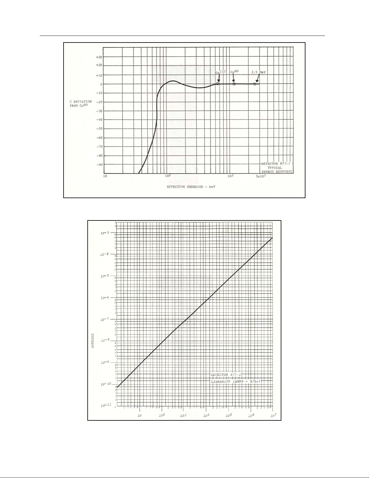
Fig rates th response for r, Figure 1-3 illustra pical linearity for
ure 1-2 illust
the d Figure radiation input er reading.
detector an
1. ent
3 Equipm Overview
H ontainm or Detecto
igh-Range C ent Monit r (877-1)
Th containm detector is a tector that has the appearance of a
e high-range
si r domed out seven inc er are two flange-mounted
x-inch diamete
el isting of haped plates, ur inches in diameter, stacked, and
ectrodes cons 31 flat, disk-s each about fo
ounted on disk rods. The assembly has the appearance of a large air capacitor. The mounting posts are
m
attached to the mounting flange throug
respect to the charges applied to the electrodes.
The whole assembly is covere
mounting flange. The mounting
for exhausting and back filling the chamber. The oth
el ted to the neutral mounting flange. When the coaxial signal
ectrode. One pin in each pair is connec
ca cable shield is connected to the neutral pin.
ble is connected to this connector, the
tions (c lt factory) Rea
e typical energy
1-4 illustrates
ent monitor
cylinder ab
h insulating spacers, so the flange and housing will be neutral with
d by the six-inch diameter housing which contacts only the neutral
flange is pierced by three holes. One hole supports the exhaust tube used
876-1-55, Rack Ch
a
tputs: 0 -
0 0 0 -
the detecto
versus met
n ion chamber de
hes long. Inside the cylind
er two support two 2-pin connectors, one for each
tes ty
T and nitrogen at atmospheric pressure and sealed.
he entire chamber is filled with a mixture of helium
F r to Section 4, Functional Description.
or further information refe
Readout Module (876A-1)
The 876A-1 Readout Module is designed to giv
ithin the ntainment area. The readout is c
w co omposed of an analog meter, indicator lights and operating
switches. The meter has a range of 1 to 10 R/h and is controlled by an eight position rotary switch. The
readout is mounted in the 876-1-55 Rack Chassis located in the cont rol room.
For further information refer to Section 4, Functional Description.
e an indication, on an analog meter, of radiation levels
7
Rack Chassis (876-1-55)
The 876-1-55 Rack Chassis permits mounting of two readout modules or one readout module and one
optical isolator in a 19-inch wide RETMA equipment rack. The panel height is 5.21 inches.
For further information refer to applicable drawing located in Appendix C.
Pull Box Assembly (878-12-5)
1-3
Page 9

Victoreen 875 High Range Containment Monitor
Operator Manual
T
he 878-12-5 Pull Box Assembly is designed to allow for thermal expansion of the detector cables and to
p a service loop. Various optional pull-box configurations are available per Table 1-1. Fo r more
rovide
in
ion refer to Section 2, Appendix B, and Appendix C.
format
able 1
T
-1. Pull-box Variations
Model Inlet, Size and Location
878-12 1" 270° 2, ¾", 90° 180°
878-12-M 1 1" MNPT 270° 2, ¾", 90° 180°
878-12-M2 1" MNPT 270° 2, 1", 90° 180°
878-12-M3 1" 270° 1, 1", 90° 180°
878-12-M4 1" 270° 1, 1", 90° 90°
878-12-M5 ¾" 270° 2, ¾", 90° 180°
878-12-M6 2, ¾" 0°/360° 2, ¾", 90° 90°
878-12-M7 1" MNPT 270° 2, ¾", 90° 90°
878-12-M8 2, ¾", 0° 1,1", MNPT, 90° 90°
878-12-M9 1,1" MNPT 90° 1, ¾" MNPT, 120° 150°
1, ½" MNPT, 210° 210°
878-12-M10 1,1" MNPT 2, ¾ 90° 0°
878-12-M11 2, ¾", 90° 1,1" MNPT 90° 0°
878-12-M12 2, ¾", 270° 1" MNPT, 0° 90°
Outlet, Size and
Location
Inlet/Outlet Orientation
Flexible Tubing (878-12-30TAB)
.0 inch diameter flexible stainless steel tubing is available in various lengths to interconnect the 877-1
1
etector to the first pull-box.
D
ables/Connectors/Panel
C
In-Containment Cable: (878-1-9-TAB)
Ex-Containment Cable: (50-103-TAB)
Replacement Detector Co
Blank Panel: (844-8-5)
nnector Kit: (878-7-5)
Optional Equipment
The following optional equipment is available:
878-10 Field Calibrator - 250 mCi
137
Cs
1-4
Page 10
General Information
Equipment Overview
Figure 1-1. High-Range Containment Monitor 875
1
1-5
Page 11
Victoreen 875 High Range Containment Monitor
Operator Manual
Figure 1-2. Typical Energy Response Curve – Detector 877-1
Figure 1-3. Typical Linearity Detector 877-1
1-6
Page 12
General Information
Equipment Overview
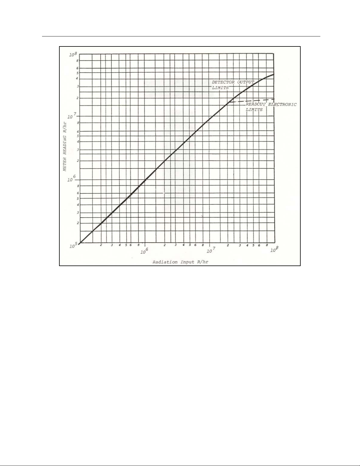
Figure 1-4.
Radiation Input vs. Meter Reading (Calculated Curve)
1
1-7
Page 13
Victoreen 875 High Range Containment Monitor
Operator Manual
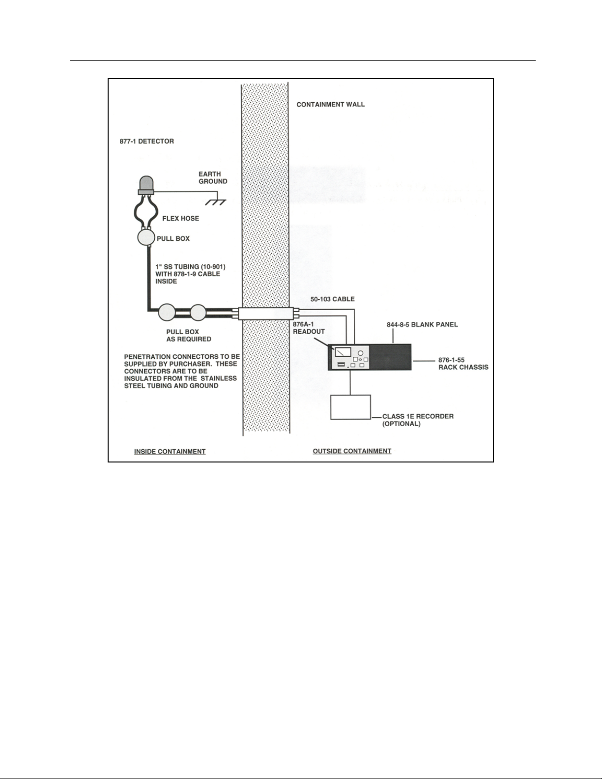
Figure 1-5. High-Range Detector, Recommended Installatio
n
1.4 Receiving Inspection
Upon receipt of the unit:
1. Inspect the carton(s) and contents fo
notify Fluke Biomedical at 440.248.9300.
2. Remove the contents from the packing material.
3. Verify that all items listed on the packing list have been received and are in good condition.
If any of the listed items are missing or damaged,
notify Fluke Biomedical.
1-8
r damage. If damage is evident, file a claim with the carrier and
NOTE
Page 14

General Information
Storage
1
1.5 Storage
Storage of Victoreen instruments must comply with level B storage requirements as outlined in ANSI
N45.2.2 (1972) Section 6.1.2(.2). The storage area shall comply with ANSI N45.2.2 (1972) Section 6.2
Storage Area, paragraphs 6.2.1 through 6.2.5. Housekeeping shall conform to ANSI N45.2.3 (1972).
Level B components shall be stored within a fire resistant, tear resistant, weather tight enclosure in a wellventilated building.
Storage of Victoreen instruments must comply with the following:
1. Inspection and examination of items in storage must be in accordance with ANSI N45.2.2 (1972)
Section 6.4.1.
2. Requirements for proper storage must be documented and written procedures or instructions must
be established.
3. In the event of fire, post-fire evaluation must be in accordance with ANSI N45.2.2 (1972), Section
6.4.3.
4. Removal of items from storage must be in accordance with ANSI N45.2.2 (1972), Sections 6.5 and
6.6.
1.6 Procedures, Warnings, and Cautions
The equipment described in this manual is intended to be used for the detection and measurement of
ionizing radiation. It should be used only by persons who have been trained in the pro per interpretation of
its readings and the appropriate safety procedures to be followed in the presence of radiation.
Although the equipment described in this manual is designed and manufactured in compliance with all
applicable safety standards, certain hazards are inherent in the use of electronic and radiometric
equipment.
WARNINGS and CAUTIONS are presented throughout this document to alert the user to potentially
hazardous situations. A WARNING is a precautionary message preceding an operation that h as the
potential to cause personal injury or death. A CAUTION is a precautionary message preceding an
operation that has the potential to cause permanent damage to the equipment and/or loss of data.
Failure to comply with WARNINGS and CAUTIONS is at the user's own risk and is sufficient cause to
terminate the warranty agreement between Fluke Biomedical and the customer.
Adequate warnings are included in this manual and on the product itself to cover hazards that may be
encountered in normal use and servicing of this equipment. No other procedures are warranted by Fluke
Biomedical. It shall be the owner’s or user's responsibility to see to it that the procedures described here
are meticulously followed, and especially that WARNINGS and CAUTIONS are heeded. Failure on the
part of the owner or user in any way to follow the prescribed procedures shall absolve Fluke Biomedical
and its agents from any resulting liability.
Indicated battery and other operational tests must be performed prior to each use to assure that the
instrument is functioning properly. If applicable, failure to conduct periodic performance tests in
accordance with ANSI N323-1978 (R1983) Radiation Protection Instrumentation Test and Calibration,
paragraphs 4.6 and 5.4, and to keep records thereof in accordance with paragraph 4.5 of the same
standard, could result in erroneous readings or potential danger. ANSI N323-1978 becomes, by this
reference, a part of this operating procedure.
1-9
Page 15

(Blank page)
Page 16

Installation
Cable and Wiring Installation
Section 2
Installation
2.1 Installation
Installation of the monitoring system consists of selecting suitable mounting sites for each component of
the system, mountin
configuration.
Installation of this system is as follows:
g each of the components, and connecting the components into the system
NOTE
2
Refer to the applicable drawings
further ins
Rack Chas
The 876-1-55 rd 19-inch chassis with a flame barrie
is required fo upport brackets
the rack esigned to mount on the 19-inch qu alified equipme
Recomm n drawings GEL876-1-55, and 876-1-114.
Readou
Readout Module 87 to fit into one-half
odule in the rack chassis (see draw en insert and tighten the two holding screws in
m ing GEL876A-1), th
the rear flanges of the ra The pawl fastener on the front
tightened.
Optical Isolat
sis
Rack Chassis is a standa r. When seismic qualification
r the readout, seismic s (P/N 876-1-114) are needed to supp ort the rear of
chassis. The brackets are d nt rack.
ended mounting is shown o
t Module
6A-1 is designed of an 876-1-55 Rack Chassis. Insert the readout
ck chassis. panel of the readout must be
or (No longer manufactured, consult factory)
tallation Instructions.
in Appendix C for
Detector
NOTE
The detector case MUST BE PHYSICALLY
GROUNDED TO EARTH GROUND. The readout
instrument circuit common SHOULD NOT be
grounded to earth ground.
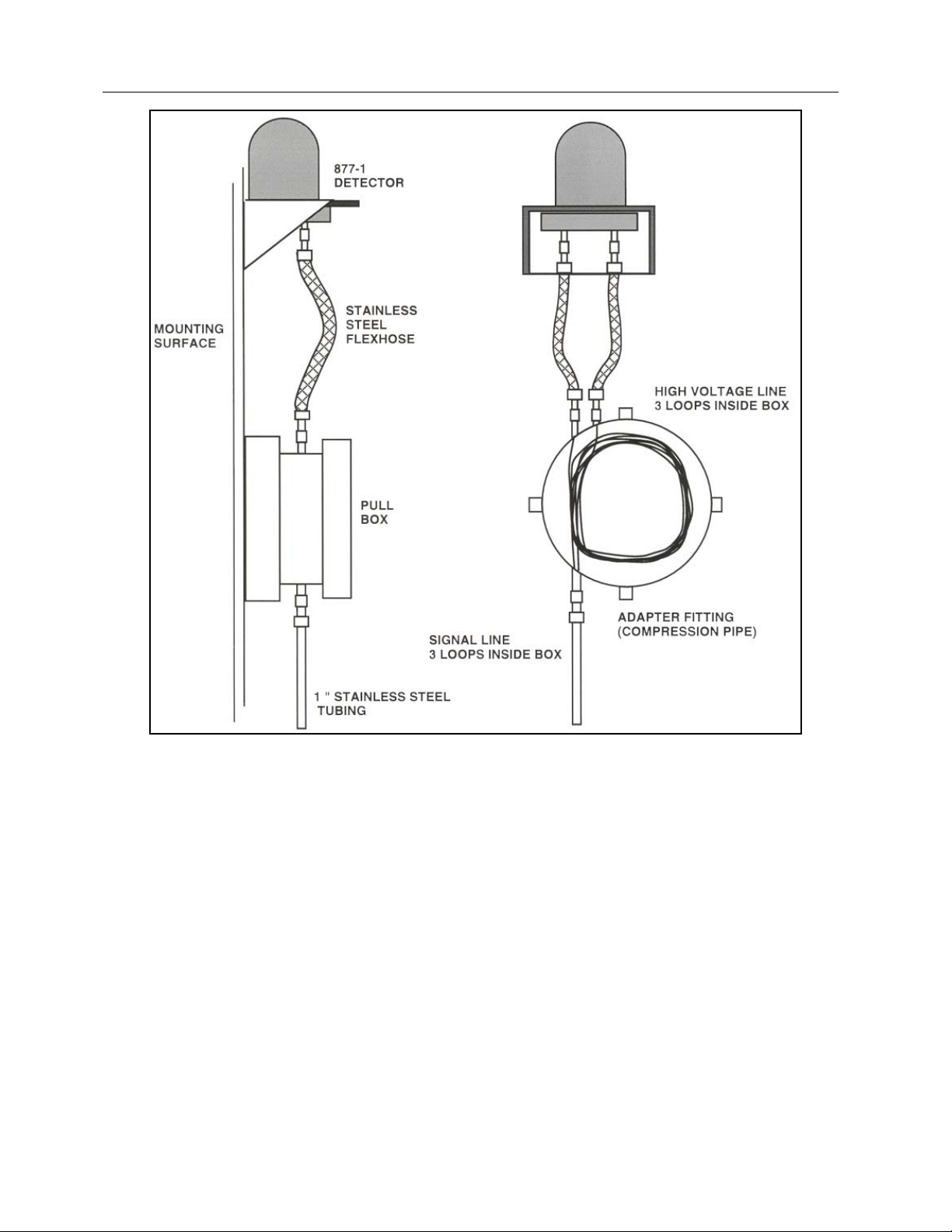
The 877-1 Detector is designed to mount on the c ent wall. A mounting bracket attached to the
detector has four holes that are used for mountin must be placed in the containment wall before
mounting the detector. D the holes in the
mounting bracket (refer ade 5. No lock
washers are to be used detector so that the
cable connectors are on amps
rovided, securing the b of 132 in. lbs. (Figure 1-5 and GEL877-1).
imensions for the studs are the same as the dimensions of
to drawing GEL877-1). Recommended studs are 5/16 inch Gr
and recommended torque for the nuts is 18 ft. lbs. Orient the
the underside. Attach the detector to the mounting bracket with the four cl
olts with a torquep
ontainm
g. Studs
Pull Box
A cable pull box is required to allow for thermal expansion of the detector cables and to provide a service
ld be loop. The pull box (drawing 878-12-5) is a typical type that mounts to the containment wall. It shou
mounted directly below the detector as shown in Figure 1-1. Depending on actual detector location
than one pull
box may be necessary.
, more
2-1
Page 17

Victoreen 875 High Range Containment Monitor
Operator Manual
NOTE
Under potential L.O.C.A. conditions of pressure and
temperature, the cable may expand as much as 11
inches per 100 feet.
The distance from the p
th
e detector cables. Additional information is found in the paragraph below Cable Sealing and in CABLE-
877 and 878-12-3 procedures in Appendix B.
ull box to the detector will be determined by the amount of flex hose used to seal
Once the cables have been pulled and tested, the pul
shut, follow the steps outlined in procedure
304 stainless steel.
878-12-3 in Appendix B. Pull box material type and grade is
l box cover must be bolted shut. To bolt the pull box
Cable Sealing
In-containment cable is 878-1-9. This is special cable designed to withstand the potential hig h radiation
that may exist following a L.O.C.A. or similar event. In order to withstand the high pressure and moisture
generated during such an event, the entire cable length must be sealed so that moisture will not come in
contact with the cable. Cable specifications are listed below.
Specifications for Cable 878-1-9
Conductor
Insulation Tefz
Shield #36 AWG, Tinned copper brand, 90 % Coverage
Jacket Tefzel (BIWF)
Outside Diameter 0.250 to 0.295 in
(6.35 to
Impedance 75 ohms nominal
Capacitance 22 pf/ft nominal
Dielectric Strength 7000 V minimum
#24 AWG, 19/36 Tinned Copper
el (BIWF)
7.49 mm)
Operating Voltage 2300 V maximum
The following guidelines are based on
lex Hose 878-12-30, ¾ inch dsteel F iameter x 18.5 inche
should ctor and pull box. St
installed from etration for each cable
used, a one (1) inch diam ded.
be installed between the dete ainless steel tubing (¾ inch diameter) should be
the pull box to the pen . If a common stainless steel tubing run is
eter tube is recommen
the sealing method used during the qualification test. Stainless
s long (with welded Swagelok connectors)
NOTE
Seismic su technique at
penetration requirements.
Technique e customer's
responsibilit
Attach the sta e pull box with compression fitt
tightening, tig e flex hose connection at the pull box is
manner. The dete hose is swaged to the cable co
done until cable is pull (Refer to the proc
information.)
2-2
inless steel tubing to th ings (¾ inch) and, after finger
hten at least 1-¼ turns. Th installed in the same
ctor end of the flex nnector backshell. This should not be
ed and tested. edure Cable-877, in Appendix B, for more
pport and the sealing
vary with plant
s and materials used are th
y.
Page 18

Installation
Cable and Wiring Installation
NOTE
Minimum bend radius of the 878-1-9 cable is four
inches. When bending conduit or flex hose, take
this into consideration. Typical bend
radius for P/N
878-12-30 is ¾ inch; stainless steel flex house is 12
in
ches.
.2 Cable and Wiring Installation
2
etector Cable I ide Containment
D ns
etector cables used inside c ccording to procedure
D ontainment are to be installed and terminated a
able-877, in Appe any moistu ts to depos nectors used
C ndix B. Do
r installing cables l for ele e det s extremely
small current tions the tratio
ust be shielded but not grounded (qualified butt splices are acceptable). Refer to drawing GEL875-1 for
m
lectrical connectio and to 878-1-9 for cable .
e ns data
due to the potentia
signals, no terminal block connec are acceptable in pene n. Signal conductor
not allow re or contaminan
ctrical leakage. Becaus
UTION
CA
it on the con
ector transmitfo the
2
The detector and readout must not be connect
during the following
Detector Te
esting of detector T cab equire rom cente
hield should yield better than 1000 megohms at 1000 VDC.
s
Typical resis .022 o C (68 ).
etector Cable O side C ntainment
D ut o
Detector cabl uld b l ty G 59
hould connect dire from e penetration to appropriate connectors on Readout Module 876A-1.
s ctly th the
erminal block con tions and unshielded ce onductors are not epta r installation. Fluke
T nec nter c acc ble fo
Biomedical recommends that cable 50-1 shown on drawing GEL 875-1. After
stallation, testing is required scribed in the previous paragraph. Specifications for cable used
in as de
utside containmen are liste Refer to drawing 50-103 for addi al da .
o t d below. tion ta
pecifications fo Cable
S r 50-103
Type RG 59/U, alternate
Conductor
Insulation
Flame Tape
Shield #36 AWG, 92% coverage
st After Installation
les after installation is r d. A leakage test f the r conductor to the
tance of the center conductor is 0 hm per foot at 20° °F
es used outside containment sho e a qualified coaxia pe R /U. Ideally, the cable
19/36 Tinned copper
Cross-linked polyethylene
Mica tape
test.
03 be used. Typical wiring is
ed
Insulation Wrap 0.001 inch (0.03 mm) mylar
Jacket Type Bostrad 7 (CSPE)
Thickness 0.015 inch (0.38 mm) nominal
Outer Diameter 0.217 inch (5.51 mm) nominal
Impedance 75 ohms nominal
Capacitance 22 pf/ft nominal
2-3
Page 19

Victoreen 875 High Range Containment Monitor
Operator Manual
Ancillary Wiring
Ancillary wiring for computer, recorder, power and alarm contacts are installed accor
875-1 and Table 2-1 which indicates connector pin designations.
able 2-1. Installation
T
ding to drawing GEL
Function J3
Ground D
Ground F
Computer E
Recorder C
A Alert larm I N NO NC
P C C
R NC NO
Alert A NO NC larm II D
E C C
F NC NO
High Alarm I S NO NC
T C C
U NC NO
High Alarm II G NO NC
H C C
J NC NO
Fail Alarm I K NO NC
L C C
M NC NO
Fail Alarm II A NO NC
B C C
C NC NO
A Line
Neutral B
Chassis Ground C
ys are Fail Safe, i.e. energized for normal operation. Relays de-energize during an alarm condition.
* Rela
All Alarms on P2 Normal Operation * Shelf State
Computer & Recorder
Power Connections (P1)
Normally open
NO =
= Common
C
C = Normally closed
N
2-4
Page 20

Operation
Operation
3
Section 3
Operation
.1
Operation
3
nce i sly
nstallation is completed, operation is fully automatic. The 876A-1 Readout Module continuou
O
dicat s an
es the level of radioactivity measured at the detector site. When the radiation level exceed
in
larm
set point, an alarm is actuated.
a
he fo
llowing steps explain how to operate the 875 monitor:
T
1. urce
Turn the function switch to the TEST position, and press and release the Electronic Check So
(ECS) push button. About four seconds later, the SAFE-RESET light should come on. Then
and hold the CHANNEL TEST push button. The ALERT, HIGH, and CHANNEL TEST lamps
light immediately.
NOTE
When channel test is pressed, the high and alert
alarm relays are deactivated. (Their coils are deenergized). The wiring of the channel test circuit is
such that the channel test lamp will not light unless
the alarm relay contacts are in the deactivated or
tripped state. This is for the purpose of assuring
that an actual contact state change has occurred,
identifying that the channel is in the test mode.
Reconciling these alarm conditions is the user's
responsibility, since the remote alarms are not
included in the standard containment monitor
system.
Release the CHANNEL TEST push button. The SAFE-RESET lamp should stay on. Either or both
2.
of the HIGH (red) and ALERT (yellow) lamps may stay on or go out depending on the alarm reset
mode chosen by the installation of jumpers on the alarm circuit board. The monitor is supplie
the manual reset mode selected.
3. will
To reset any alarm light, press the SAFE-RESET push button. If conditions are normal, the light
go out.
4.
Switch the function switch to the ALL position.
5. ut 10
Again press the ECS push button. The panel meter indicator should go to a reading of abo
R/h and the green SAFE-RESET light stays on in the operating condition. If the panel meter shows
little or no deflection at the pressing of the ECS push button, the green light should go out fou
seconds after the ECS push button is pressed. In this case, follow troubleshooting procedures.
6. To set the alert and high alarm adjustments, remove two screws in the rear of the chassis, loosen
knurled knob on the front of the chassis, and slide the module forward part way out of th
the e rack
reveal the adjustment potentiometers R513 and R509 on the relay driver printed circuit bo
to ard. To
adjust the HIGH alarm, depress the red HIGH push button and adjust R513 (drawing 876A-1-75A)
until the meter indicates the desired alarm level. To adjust the ALERT alarm, depress the yellow
ALERT push button and adjust R509 (drawing 876A-1-75A) until the meter indicates the desired
alarm level. Return the module to its proper position in the rack. Tighten the rear holding screws.
Tighten the knurled holding knob on the front. Return the module to service.
press
should
d with
r
3
3-1
Page 21

Victoreen 875 High Range Containment Monitor
Operator Manual
During normal operation, the radiation field is usually less than 1 R/h (the lower limit of detection of the
high range detector) and the analog meter display will be at the low end of the meter sc
ale.
Figure 3-1. Readout Module 876A-1, Front and Rear View (reference only, not to scale)
3-2
Page 22

Function Description
Functional Description
4
Section 4
Function Descriptio
4.1 Functional Description
High-Range Containment Monitor Detector 877-1
The high-range containment monitor detector is an ion chamber detector that has the appearance of a
six-inch diameter domed cylinder about seven inches long, mounted on an L shaped bracket. Inside the
cylinder are two flange-mounted electrodes consisting of 31 flat, disk-shaped plates, ea
inches in diameter, stacked, and mounted on disk rods. The 31 disks form two groups, interleaved wit
each other, 16 collection disks and 15 signal disks. Because of the interleaving, they appear as only on
stack, but the collection disks are mounted on three collection disk-posts and the signal disks on three
signal disk-posts. Spacers on t
clearance holes in the disks allow posts of the opposite polarity to pass through without conta ct. The
assembly has the appearance of a large air capacitor. The mounting posts are attached to the mounting
flange through insulating spacers, so the flange and housing will be neutral with respect to th e charges
applied to the electrodes. The collecting diskposts are elongated beyond the last collecting disk to support
a cup-shaped liner having the same potential as the collecting disks, thus becoming part of the collector.
The whole assembly is covered by the six-in
mounting flange. The mounting flange is pierced by three holes. One hole supports the exhaust tube use
for exhausting and back filling the chamber. The other two support two 2-pin connectors, one for each
electrode. One pin in each pair is connected to the neutral mounting flange. When the coaxial signal
cable is connected to this connector, the cable shield is connected to the neutral pin.
he posts keep the disks separated so they do not come in contact, and
ch diameter housing which contacts only the neutral
ch about four
n
h
e
d
The entire chamber is fille
sealed.
d with a mixture of helium (2%) and nitrogen at atmospheric pressure and
The seal on this chamber must not be broken. To
do so would alter the calibration and specifie
energy response of the system.
4.2 Readout Modu
Drawings 876A-1-3H and 876-1-3A serve as
interconnecting diagrams for trac
betw
876-1-3A contains the main power supply
CAUTION
d
le 876A-1
NOTE
ing signals
een printed circuit boards. In addition, drawing
4-1
Page 23

Victoreen 875 High Range Containment Monitor
Operator Manual
PreamplifierIMeter Printed Circuit Board (P/N 876A-1-86, Schem
The detector current, measuring from 7 x 10
the reading range, enters the readout on rear panel connector J1. From the rear panel, the ion chamber
current enters the preamplifier circuit through terminal J302. It passes to U301, a seven-decade
logarithmic amplifier, where it produces an output voltage of 5 V for minimum currents and -2.6 V for
maximum currents. This voltage can be monitored at TP501, on the relay driver PC Board.
-11
to 7 x 10⁻⁴ amperes respectively, at the bottom and top o
atic 876A-1-3E)
f
Q301A and Q301B have their bases connected to their collectors, so that they operate as diodes. Q30
limits over-range inputs to
keeping the current from falling below 1 % of the lower limit of sensitivity. This limiting of the low leve
current speeds the response of the logarithmic amplifier. The output of U301appears on terminal 13 of
J301. This terminal is connected to terminal 13 of J103 on the motherboard by a ribbon cable. From this
point, connection is made to terminal 14, J106 of the relay driver printed circuit board. This terminal is
effectively the point of input to the meter circuit and high and alert alarm circuits.
Amplifier and meter circuits can be tested by turning the function switch to TEST and depressing the
CHANNEL TEST push button on the front panel. This applies 15 volts to a circuit of which Q302B is a
series element; the purpose is to generate an input current for U301 (at pin 2) su ch that panel meter
M401 will be driven full scale.
Panel meter M401 may be switched into anyone of six positio
is determined by the voltage applied to pin 10 of U401 from pin 3 of J401. U401 is driven in turn by U5
of the relay driver printed circuit board. Connection is made from terminal 12 of the relay driver printed
circuit board to terminal 3, J401 of the preamplifier metering printed circuit board through pins 11 and 14,
J101 of the switchboard (drawing 876-1-3J) so that the signal path may be interrupted when it is desired
to use the meter for alarm setpoint checks.
One of the six sensitivity positions, the ALL position, displays all seven decades on the red meter scale.
Each of the other
addition there is a TEST position and an OFF position. The TEST p
positions expands the scale to achieve a three-decade display on the black scale. In
U301. Q302A is a lower-level clamp on the input to logarithmic amplifier U301,
ns of different sensitivity. The meter current
osition is also a seven-decade meter.
1
l
01
Power Supplies
Mother Board Power Supplies (P/N 876-1-78, Schematic 876-1-3A)
T101 acts as a step down transformer producing an o utput voltage of 24 VDC. This is rectified in the fullwave rectifier consisting of four diodes, CR101 through CR104. The 0.1 microfarad capacitors on the AC
input suppress spikes and limit noise. The output of this 24-volt supply provides the power to both the
positive and negative power supplies o
n the power supply printed circuit board.
Printed Circuit Board Power Supplies (P/N 876-1-89, Schematic 876-1-3C) (P/N 876-1-89A,
Schematic 876-1-93A)
Positive Power Supply
Twenty-four
circuit U2 is a voltage regulator; +15 V comes out of pin 2 of U2. A second supply of +14 volts is pro
through pass element Q1. This output serves relays, lights, and other high current circuit elements. It is
current-limited through R29. The 14 V supply is monitored at TP3.
(24) V power from the motherboard enters the power supply board on terminal 1. Integrated
vided
Negative Power Supply
Transistors Q7 and Q8 make up a free-running multivibrator with a 9 kHz repetition rate, which is powered
by the unregulated 24 volts from the motherboard power supply. Q6 acts as a current limiter for this
multivibrator. U1, pins 8, 9, and 10, and Q5 accept its output and act as a driver stage for the rectifier
which follows. This rectifier consists of CR4 and CR5, and produces a negative voltage, which should be
about -21 VAC, and can be measured at TP5. Voltage regulator U1 (located on the 876-1-89A add-on PC
board) takes this voltage as an input, and delivers a -10 V regulated voltage, which is obtained from
terminal K of the board, and can be monitored at TP4.
4-2
Page 24

Function Description
Readout Module876A-1
High Voltage Power Supply Normal Operation (non-ECS Test)
The multivibrator circuit of Q7 and Q8 also supplies the input to the high voltage generator. Two of the
transistors of U1 act as buffers between the multivibrator and the high voltage circuit. Q4 and Q3 serve a
output driving stage for the primary of high voltage transformer T1. The i
approximately 12.5 V peak to peak. T1 has a step-up ratio of approximately 20: 1. C22, C
C20 form a voltage doubler that gives a DC output of approximately 525 volts. The resistor capacitor
circuit R42, R43, and R44, and C17, C18, and C19 serve for further filtering, and ultimately a 506 volt
output is delivered at J1.
nput to T1 is a square wave,
R15, CR14, and
4
n
R37, R40 and R41 form a voltage divider across the 515 V input to the resistor capacitor filter. The
voltage at the junction of R37 and R40 is the input to OP AMP U2 pins 6 through series resistor R39. Pins
5 and 6 of U2 are the inpu
high voltage.
U2 (pins 1, 2, 3) is used as a logic c
Comparison Circuit on Power Supp
ECS test, and a muting
checking circuit during the ECS test, and is described in more detail in the "FAIL/SAFE" paragraph.
ts to a difference amplifier, which acts to produce additional regulation of the
ircuit in the SAFE/FAIL circuit of the monitor, refer to FAIL/SAFE
ly Board for additional information. In addition to the 6.2 V reference
resent at terminsignal, a voltage will be p
signal will also be present at terminal M. This circuit is a part of a complex
al P that comes from terminal 8 of the ECS board during the
Operation of High Voltage Supply During ECS Test
A low voltage ramp (approximately 0 to 6.2 V) from the ECS board enters the power supply board on
terminal 12, and proceeds through a series of auxiliary circuits to give a ramp of the same waveshape on
the center-tap of the primary of high voltage transformer T1, which point is also the source of power to the
driving circuit Q3 and Q4. As a result of this variation of the voltage at the center-tap, the amplitude of the
current in the primary varies accordingly, and ultimately the voltage output at J1 varies from 0 to 506
volts, linearly with time. This high voltage ramp generates the current in the detector circuit during the
ECS test period.
FAIL/SAFE Comparison Circuit on Power Supply Board
The comparison circuit on the power supply board, consisting of U2, pins 1, 2, and 3 has two functions
he first function, a monitoring of the high voltage, is in operation at all times except during the ECS test
T .
this voltage falls below 80
If % of its rated value, (roughly, from 500 to 400 volts), the FAIL/SAFE circuit
ill go out, and the FAIL relay will de-energize. During this period, a steady 6.2 volts, which is input on
w
rminal 13, serves as a comparison voltage. The voltage on pin 2 is proportional to the high voltage
te
h a high ratio voltage divider.
throug
:
The second function, a monitoring of the result of the ECS test, is in operation during this test. Du
period, the high voltage falls well below 400 volts (actually, practically to zero) so the monitoring of
high voltage
conditions.
On pin 2 there is impressed a positive 15-volt signal that lasts for
seconds). The voltage o
shape that creates this condition on terminal M is ca
whatever voltage would otherwise be present through the high ratio voltage divider from J1.
On pin 3 of the comparison circuit there is impressed a DC voltage that is either 6.2 volts (safe condition)
or 15 volts (fail condition). This voltage arrives on terminal P of the power supply board from a latch circuit
on the ECS board, which circuit will be described in connection with that board. A safe condition causes
the output on terminal N (from pin 1 of U2) to be -10 volts; a fail condition causes it to be +15 volts.
Terminal N is connected to the SAFE/FAIL circuit on the relay driver board, which controls the action of
the fail relay and the SAFE-RESET green lamp on the panel. A fail condition causes the green lamp to go
out and de-energizes the fail relay, although the
(6) second ECS test period. For the safe condition the green light is on, and the fail relay is energized.
as in the above paragraph is inapplicable. Instead, the following are the input and output
the duration of the ECS test (6.0
n terminal M is 15 volts during the ECS test and zero at all other times. The wave
lled the muting signal wave shape. It will override
muting signal delays these actions until the end of the six
ring this
the
4-3
Page 25

Victoreen 875 High Range Containment Monitor
Operator Manual
PreamplifierIMeter Board Power Supply (P/N 876-1-86, Schematic 876-1-3E)
A +6.2 V power supply contained on the preamplifier meter board has as its input the +15 V from the
power supply board. Integrated circuit U401, pins 12, 13, and
roviding a stable reference voltage. The output is adjustable by R413.
p
R
elay Driver Printed Circuit Board (P/N 876A-1-75A, Schematic 876A-1-3B)
T
he signal input to the relay driver printed circuit board which is taken from pin 13 of the preamplifier
m
eter may be monitored at this point through test point TP501. The signal enters pin 13 of OP AMP
U lifier stage can be adjusted by
501, and the output is taken from pin 14. The gain of this amp
potentiometer R503. The output of the OP AMP can be monitored at TP502; it provides inputs to:
• High Alarm circuit
• Alert Alarm circuit
• Meter buffer amplifier circuit
• Recorder/Com
puter drivers
14 is a voltage regulator with diode U402
High Alarm Circuit
The signal output to the high alarm circuit enter OP AMP U502 on pin 5. This is a difference amplifier,
whose other input (pin 6) is determined by the setting of potentiometer R513. The main purpose of this
stage is to control the high alarm threshold.
The output of the comparison OP AMP is connected, through diode CR504, to pin 6 of U503, whi ch
mainly as a power stage for the HIGH ALARM (red) panel light. The output of this stage (pin
serves as the input to the high alarm rela
The input to the high alarm relay driver stage of U503 is on pin 9, and the output is taken from pin 8.
Relay K502 is energized in the non-alarm state, and a signal above threshold serves to de-energize it.
There is a red HIGH ALARM jumper connected to the collector (pin 8) of the relay driver U503. The
following options are available with the presence or absence of the jumper when the radiation level
exceeds the threshold and triggers the alarm:
Manual Reset - The alarm will continue to be activated even after the radiation level recedes below
threshold until the SAFE/RESET indicator push button on the panel is depressed. This option occur
with the jumper in place.
Automatic Reset - The alarm will continue to be activated only as long as the radiation exceeds the
threshold level. This option occurs with the jumper removed.
The red warning light acts similarly to the alarms. It lights when the alarm relay is de-energized.
Each relay contains four Form C contacts, but only two of the four are accessible through the rear
connector.
The connection to the red panel warning light is from term
c to the colle in 7) of U503 sistor R5
onnected ctor (p through re 21.
A
lert Alarm Circuit
T m circuit enters a differen mplifier,
he signal input to the alert alar
w ther input (pin rmined by ote 509. The se of this
s to control the hreshol ut of the on OP AM d, through
tage is alert alarm t d. The outp comparis P is connecte
d 3, which acts m wer rt (yellow) panel light. The
iode CR501, to pin 13 of U50
o o serves a the ale y driver 03, whose
main functio 1. The i rt ala stage on pin 2,
and the output to the relay is taken from p 01 is he non e, and a
s bove threshold de-energ
ignal a serves to
n is to driv
2) is dete
n 14) als
e relay K50 nput to the ale
y driver stage U503, whose main function is to drive relay K502.
inal 3 of the printed circuit board, which is
OP AMP U502 o
the setting of p
ainly as a po
s the input to
K5
ize it.
n pin 3. This is
ntiometer R
stage for the Ale
rt alarm relautput of this stage (pi
rm relay driver
energized in -alarm sta
t
main purpohose o
stage U5
of U503 is
7) also
ce a
tin 1. Relay
acts
s
4-4
Page 26

Function Description
Readout Module876A-1
There is a yel
stage of U503
radiation level exceeds the threshold and triggers the alarm:
Manual Reset - The alarm will continue to be activated even after the radiation level recedes below
threshold until the S
the jumper in place.
tomatic Reset - The alarm will continue to be activated only as long as the radiation exceeds the
Au
threshold level. This action occurs with the jumper removed.
The yellow warning light acts similarly to the alarms. It lights when the alarm relay is de-energized.
Each relay contains four Form C contacts, but only two of them are accessible from the rear connector.
The connection to the yellow panel warning light is from terminal 2 of the printed circuit board, which is
connected to the collector (pin 14) of U503 through R526.
low ALERT ALARM jumper connected to the collector (pin 1) of the alert alarm relay driver
. The following options are available with the presence or absence of the jumper when the
AE/RESET indicator push button on the panel is depressed. This action occurs with
4
Fail/Safe Circuit
Input to the fail/safe circuit comes from pin 1 of U2 on the power supply board, entering the relay driver
board on pin H of the relay driver printed circuit board. The input is a DC voltage that is either high (15 V)
or low (0 V); if it is low, relay K3 is energized (non-alarm condition). If the signal is high, the green
SAFE/RESET lamp will go off and the relay is de-energized, indicating a fault somewhere in the sy
The circuit consists basically of two inverters in tandem so the voltage on
approximately the same as the input voltage, the diode CR508 preventing current flow through the
solenoid if the collector is slightly higher than the 14 V at the other end of the solenoid coil.
the collector of Q502 is
stem.
Recorders and Computer Buffers
Provisions have been made for delivering DC output voltages to a recorder and computer for further
processing. The buffers are located on the relay driver board. If a commercial device is to be conne
a signal isolator must be installed between the
both computer and recorder buffers arrive at pin R of the relay driver printed circuit board, coming from
terminal 3 on the ECS printed circuit board. The computer buffer consists of and OP AMP using pins 1, 2
and 3 of U501, the output being taken off the relay driver board at pins 4 (+) and 2 (-) of P502. Resistors
R532 and R533 act
options are shown in Table 4-1.
The recorder buffer consists of an OP AMP using pins 5, 6 and 7 of U501, the output being taken off the
relay driver board at pins 1 (+) and 3 (-) of P502. Resistors R530 and R531 act as voltage dividers for t
output. Their value for standard usage and available options are shown in Table 4-1. Both buffers are
disabled during the ECS test by a switching circuit on the ECS board, so that the ECS current is no
recorded. This circuit consists of Q201 and Q
during the ECS test.
as voltage dividers for the output. Their values for standard usage and available
device and the 876A-1 Readout Module output. Inputs to
202 on the ECS board and is activated by a muting voltage
cted,
he
t
Table 4-1. Resistance Options for Voltage Dividers
Resistor Std. Option 1 Option 2 Option 3
Recorder
Voltage
R53 200 ohms 0 1 kilohm 119.8 kilohms 200 ohms
R53 200 ohms 1 kilohm 1 kilohm 1 200 ohms
R53 0 ohms 2 200 ohms 11.8 kilohms 23.8 kilohms 20
R53 s 200 ohms 1 kilohm 3 1 kilohm 200 ohm
Computer
Voltage
0 – 1 V 0
0 – 5 V 1 – 100 mV 0 – 50 mV 0 – 5 V
– 10 mV 0 – 5 V 0 – 5V
4-5
Page 27

Victoreen 875 High Range Containment Monitor
Operator Manual
en Clamp
P
The pen clamp circuit is a CR502. It
prevents pin 9 from goin en from being jammed
clamping circuit consisting of U501, pins 8, 9 and 10 and diode
g negative. The purpose of this is to prevent the recorder p
against the baseline.
Electronic Check So hematic 876A-1-
urce (ECS) Printed Circuit Board (P/N 876A-1-92, Sc
30)
Due to the range of the /h), a remotely activated radioactive check source is
practical, since the sou and the shielding necessary for this source would
effect detector energy response. For this reason, an electronic check sour
source operation, the detector remains connected to the system as a passive cap
the current-voltage relation in a capacitor is such that the current is proportional to
th y current. It is
e applied voltage, an applied voltage, in the form of a linear ramp, will produce a stead
th
is current which is read during the ECS test.
The ECS board (drawing 876A-1-3D) has two main functions: 1. To genera
in the high voltage supply, develops the high voltage ramp responsible for the test current in the detector
during the ECS test. 2. To monitor the current flowing during the ECS test, and recognize whether the test
signifies a passing of failing condition in the circuits of the unit. One of the circuits involved in this
monitoring process is actually on the power supply printed circuit board.
The voltage ramp which develops the detector current during the ECS test rises from 0 to 506 volts ov
three seconds, so that the rate of change of voltage is approximately 170 V/second. The capacitance
the detector is approximately 435 picofarads and therefore, the steady current during the rise of the
voltage ramp is approximately 7 x 10
The ramp occurs when ECS is initiated for a period of about six (6) seconds, during which time the
system is not acting as a radiation monitor.
The ECS test may be initiated at the will of the operator. For this purpose there is a manually operated
ECS push button. If the ECS test is not initiated by the operator, it will take place automatically every 17.1
minutes. After each manually initiated test, the automatic circuits are reset so that a test will be initiated
17.1 minutes later.
detector (1 to 10E7 R
rce activity would be high im
-8
amperes, which puts the panel meter at about one-third full scale.
ce is provided. During check
acitive element. Since
the rate of change of
te the low voltage ramp which,
er
of
In addition to causing visual alarms and relay de-energizing if circuit failures are found, the ECS test
affects the panel meter as in the three cases described below. It is the processing of the voltage rea d by
the panel meter during the ECS test that is responsible for the action of the circuits directly involved in
driving the visual (green light) and relay (fail) alarm circuits. Recorder and computer outputs are muted
during the ECS and will indicate zero
while the test is in progress, approximately six (6) seconds.
Panel Meter Action During ECS Test
The meter action to be expected during the test period with the containment monitor operating prop
can best be explained by considering three initial conditions: 1) Panel meter is
end of scale; 2) Panel meter on scale but below 10
1. Meter at extreme lower end of scale
3
R/h; 3) Meter above 103 R/h at start of test.
In this case, the meter needle should remain motionless for about 1 second, rise to 10
resting at extreme lower
3
remain there for about three seconds, and then fall to its initial position.
3
2. Meter on scale, but below 10
R/h
In this case, the meter needle should fall to zero at the beginning of the test period. It will then rise
to approximately one-third full scale, and remain in this position for about four seconds. After this,
will resume its original reading, w
3
3. Meter above 10
R/h at start of test
This case is quite similar to the above except that the meter may not fall to zero at the start of the
test, and at the upswing, it will take a position higher than 10
ith perhaps some slight negative overshoot.
3
R/h, the excess depending on the
ambient radiation. It will ultimately resume the same position as before the test as in item 2 above.
erly
R/h and
it
4-6
Page 28

Function Description
Readout Module876A-1
NOTE
During the ECS test, all alarms are muted; that is,
their operation is disabled until the completion of
the test. During this six-second period there is no
warning of a high radiation condition. If this
situation is not tolerable, two containment monitors
must be installed.
Action of Green Safe/Reset Light and Alarm During ECS Test
The behavior of the green SAFE/RESET panel light during the test is as follows:
A pass condition is indicated by the green light remaining lighted throughout the test.
A fail condition is indicated if the green light goes out at the end of the test.
Circuit Actions at Manual and Automatic Initiation of ECS Test
Whether the ECS test is initiated automatically or at the will of the operator, a trigger signal is delivere
pin 4 (manual) or pin 5 (automatic) of U206, whose output initiates the low voltage ramp generation.
Automatic operation may be disabled by the removal of jumper 200A. The system will then respond on
to the pressing of the ECS button.
4
d to
ly
The circuit containing U201 (pins 5, 6, 7) and U208 (pins 11 and 12) constitutes a clock
illisecond repetition rate. It is followed by counters U204 and U205. The action of U204 is entirely
m
stricted may be
re to automatic control of the ECS test, as is the output from pin 1 of U205 (note that it
pen-cir s
o
that enter into
m
fu
) re-initiation rator
2
in
in
in
to
nput); 3) pin rator
(i
Q
xplanati
e
ow Vol
L
he elem
T
ssociated ca
a
t the arr
A
uickly to rging
q
apacito ntiometer
c
R
harge of cap tor plates.
c
cuited by the removal of jumper 200A). However, the outputs from pins 3, 5, and 6 have function
both manual and automatic action. In addition, they involve both the ramp-gen
onitori
ng functions of the ECS board, and also enter into the operation of two important auxiliary
nction test and;
s: 1) generation of a muting pulse, so that the alarms will not be set off during the ECS
prevention--that is the prevention of malfunction on manual operation in case the ope
adverte use the
stant of ECS button
itiates t 5 pin 6
the latc ; 2) pin 5, U207
205. Th
ntly presses the ECS button more than once. The monitoring function is involved beca
generation of the latch-enable pulse occurs a precise time after the pressing of the
he test (toward the end of the test, when conditions have stabilized). The path from U20
h-enable generator may be seen to involve the following points: 1) pin 10, U203
6, U207 (output) and finally pin 11, U207, whose output drives the latch-enable gene
e latch and latch enable functions will be explained with the monitoring circuits after the
on of the ramp generation.
tage Ramp Generator
ents that enter the generation of the low voltage ramp are U203, U208, U201, Q204, and
pacitors, resistors, and diodes. U203 is an auxiliary element.
ival of the trigger, Q204 serves the purpose of reducing the voltage previously at terminal 5
zero, at which instant the ramp-generator proper takes over. Basically, C210 is the cha
r, and the other components serve either as charging resistors or linear elements. Pote
227, ramp v rate of
oltage per second adjustment (RAMP V/SEC ADJUST), serves to determine the
acitor C210, and consequently, the rate of rise of the voltage applied to the detec
with a 0.976
eration and
he ra only 6.2
mp that is generated by the ramp generator appears at terminal 5, where its maximum is
T
olts. Fro d circuit
v
oard, wh scription of
b
e power supply printed circuit board.
th
m terminal 5, it is connected to the high voltage generator on the power supply printe
ere it controls the generation of the high voltage, as explained in the functional de
4-7
Page 29

Victoreen 875 High Range Containment Monitor
Operator Manual
Monitoring Circuits of The ECS Board
The input to the monitoring ci
on terminal 1 is effectively proportional to the current produced in the detector by the application of the
rcuits of the ECS board is on terminal 1, the output on terminal 8. The input
high voltage ramp. The ov
p
ower supplies; and the SAFE/FAIL circuit on the relay driver printed circuit board.
Ultima the charge integration adjustment potentiometer (CHA RGE INTEG.
tely, by the action of R218,
A of
DJ.), charging capacitor C209, and other auxiliary elements, a DC voltage is produced on terminal 10
U20
1, and an output voltage on pin 8 which results in an input to pin 10 of U208 which will be
ap on
proximately zero if the system is operative, and approximately + 15 V it a malfunction is present, or
ch
annel power-up before the first automatic or manually initiated ECS test.
This s
ignal is the input to the latch-and-flop circuit composed of the NOR circuits U202 (pins 1 to 13). The
latch i f
s quiescent until triggered near the end of the ECS test period by the latch-enable input on pin 1 o
U202. ss indication to a fail
This trigger voltage will cause the output (pin 10 of U202) to flop from a pa
indication if a malfunction exists in the detector cable, or signal input circuit.
If the system is operative, a voltage that is low (6.2 V) will appear at terminal 8; if the system has a
malfunction, a voltage that is high (+15 V) will appear at this terminal (+15 V will appear momentar
immediately after power on). This voltage determines the action of a comparison circuit U4A, and the
output of U4A determines the action of the SAFE/FAIL circuit.
A block diagram of the entire monitoring circuit of the ECS test is shown in Figure 4-1.
erall circuit that monitors the ECS test also includes U2, described with the
ily
Figure 4-1. Block Diagram of ECS Test
4-8
Page 30

Function Description
Readout Module876A-1
4
Safe/Reset Sub-circuits
The three sub-circuits described below are all involved in the operation of the green SAFE/RESET lamp
and its associated alarm:
1. A latch for the SAFE/RESET lamp built around four NOR circuits of integrated circuit U202, with
several auxiliary elements.
2. A threshold detector U201 (pins 8, 9, and 10) ascertains by comparison with a standard voltage
whether the current produced by the ECS ramp is sufficiently high.
3. A one-shot multivibrator, U207, pins 9 to 15, which provides an enable signal to allow the latch
circuit to flop from a pass to a fail condition if the signal from the threshold detector is a fail signal.
This enable signal is necessary because the detector current during the ECS test is higher than the
average normal radiation current. The monitoring circuits must therefore be examined ju st at the
proper time, which is immediately after the cessation of the ECS current.
It will be noted that a trigger signal from the counter U205 is applied to the base of Q207, whose collector
is connected to Q203. . The purpose of this sub-circuit is to short-circuit capacitor C209, so that the
integration of the ECS may proceed from a stable and repeatable starting point. If the system is a
functioning properly, a 2.57 volt level will be present at terminal 1 at the top of the ramp, corresponding to
the 103 R/h meter indication. If voltage at pin 1 is below 2.48 V at this point, ECS circuitry will indicate
channel failure. See Figure 5-1 and drawing 876A-1-3D. This voltage, applied to the integrator circuit
consisting of R218, R224, C209 and the OP AMP circuit U201, pins 12, 13 and 14, produces a linearly
failing voltage of about 2 V/second at pin 14 of U201. This voltage begins just above 0 V. When it reaches
-6.2 volts, a quick switching action takes place in U201, the important result being a sharp change in the
output voltage (pin 8) from +15 to 0 volts. A low (approximately 0 V) input at pin 10 of U208 results
ultimately in a safe report (green light stays on and the alarm relay is energized); whereas a high
(approximately 15 V) input results in a fail report (green light goes out and alarm relay is de-energized).
For any change in the output of the latch circuit (pin 10 of U202) an enable pulse is required. This signal
is output by one-shot multivibrator U207, pin 9, which receives its input from one of the outputs of the
muting multivibrator U207 (pins 1 to 8).
Muting Circuits of ECS Board
During ECS test, it is possible that the normal current generated by the ECS voltage ramp will exceed the
trip-level chosen for the high and/or alert alarm circuits. To avoid an unwanted alarm, the alarm circuits
are muted during the ECS test--that is the alarm circuits are made inactive, so that their lamps and alarm
relays will not respond during the test. Effectively, this is done by generating voltage pulses in the ECS
circuits which last for the duration of the test, and applying them at appropriate points in the alarm circuits
on the relay driver board, so that the alarm circuitry will be momentarily disabled. Computer and recorder
buffers are also muted during the ECS test.
The circuits of the ECS board that generate the muting pulses are, to some degree, involved with the
ramp-generating and monitoring circuits of the ECS board, since all must be in time synchronization.
Generally speaking, however, the most important elements of the muting circuits are contained in
integrated circuit U207 (pins 1 to 8) and integrated circuit U206 (pins 9 to 15). The muting pulse is a
voltage which starts from zero, rises abruptly to +15 V, lasts about six seconds, and falls abruptly to zero.
Initiation takes place on pin 5 of U207, and the output is taken from pin 13 of U208. The signal for muting
the alarms appears on terminal 9 of the ECS board, but a second path leading to pin 12 of U203 serves
the auxiliary purpose of preventing re-initiation of the manually generated trigger produced by pressing
the ECS button on the panel.
4-9
Page 31

(Blank page)
Page 32

Maintenance, Calibration, and Troubleshooting
Maintenance
Section 5
Maintenance, Calibration, and Troubleshooting
5.1 Maintenance
5
The monitor is designed to ope
replacement schedule should k
very five years - Replace the 4 capacitor, P/N 92-3005-A (C1 01), and the RFI
E 200 microfarad electrolytic
e filter, P/N 92-9015A (FL101 other board of the 876A-1-108 or 876A-100
lin
R
eadout Module.
henever detector cables are re
W
co
nnectors as described in the CABLE-877 procedu
r n the containment without attention. The following
ate for long periods i
e uble-free operation.
ep the monitor in tro
), located on the 876-1-78 m
moved - Replace the nickel seals, P/N 877-1-60-1, on the detector
re in Appendix A.
Calibration 5.2 Field
The monitoring systems req
recalibrated at regular interv
should be ions personnel. For further calibration informatio n, refe
calibration Appendix A.
he high-range containment are calibration prior
T a monitor underwent a complete electronic and isotopic
to leaving the Fluk plant. The electroni
supplied in th primary iso
(greater than
capability of m
recommended:
Detectors shall either be returne
or the own procedure to determine
calibrator respon deviate from original
To encompass Nu
test. The repro
Concerning the
known decay ch
positioning, calibrator pu g tension and the
if the reproducibility of th
damaged.
Electronic
TP876A-1
test. The Readout should be c rce to verify its ability to measure the input
current accu 10 %.
determined by operat r to the applicable
procedure provided in
e Biomedical c calibration procedure for the 876A-1 Readout is
is manual. Prior to topic calibration, the detector's hermetic seal, insulation
d capacitance are opic calibration requires a highly radioactive source
400 curies) with National Bureau of Standards (NBS) traceability. As this is beyond the
ost facilities to perform, the following method of verifying detector calibration is
er must establish a that the average A/R/h output current or field
se, does not factory calibration by more than ± 20 %.
reg-0737 guidelines, on-site in-situ calibration checks can be perfo rmed with the 878-
Fie10 High-Range
ld Calibrato producing a 10 R/h indication on the channel under
ducibility of the in +/- 20 %.
878-10 Field C he 877-1 Detector, its reproducibility is based on the
aracteristics o e, the mechanical tolerances of the calibrator, detector
alignment of the 87 nal Test Procedure,
-108 included in App -1.
nnel must be fully knowl pting to perform the
rately to within +/-
e libration before placing them into service. In addition, they should be
uir ca
als ring routine service. The length of time between calibration intervals
du
verified
r that is capable of
calibrator is with
f the
ll strin skill of the user. Factory recalibration is recommended
e decayed output value exceeds +/- 20 %, or if the unit has been physically
6A Readout may be performed using Functio
edgeable in the operation of the readout prior to attemPerso
alibrated with a current sou
. Primary isotresistance an
d to Fluke Biomedical at a five (5) year interval from the date of delivery
alibrator used with t
137
Cs sourc
endix A, and the standard test equipment as listed in Table 5
5-1
Page 33

Victoreen 875 High Range Containment Monitor
Operator Manual
NOTE
Disconnect
Detector 877-1 from Readout Module
876A-1 by removing cables from J1 and J2 before
starting electronic calibration.
Table 5-1. Recommended Tes
Current Generator - Test Electrometer
Range 1 x 10
Accuracy, Current Generator
Accuracy Test Electrometer
Adjustable AC Voltage Source
Maximum Voltage Low range 140 VAC, high-range 280 VAC
Frequency 60 Hz
4 ½ Digit Digital Multimeter
Fluke 8600A or equivalent
Ranges + 0 to 100 mV up to + 0 to 100 V (20 % over-range)
Accuracy
In put Impedance > 10 megohms
D C Voltage
AC Voltage
DC Current
Carbon Composition Resistor
Resistance 10 kilohms, ½ W, 5 %
Lead Connectors Small alligator clips
DC Power Supply
Output Voltage 0 to + 25 VDC
Output Current 0 to 600 mA
L
oad Regulation
A it Down to 10 mA djustable Current Lim
M nter ulti-function Cou
F luke 1900A or equivalent
Frequency 5 Hz to 80 MHz (0.1 to 100 Hz Resolution)
Period 5 Hz to 1 MHz, single and multiple period averages
(1 to 100 nsec resolution)
Total Counts 1 to 999,999 counts
t Equipment
-12
Amps to 1 x 10⁻³ Amps
-12
Amps ± 10 %
10
-11
Amps ± 3 %
10
-10 -7
10 to 10 Amps ± 2 %
-7
to 10-3 Amps ± 0.2 %
10
± 0.2 % ± 1 digit with integration time long enough to accumulate 3
significant digits of volts indicated on display V/R ± 0.2 % ± 1 digit
100 mV range: ± (0.05 % of input ± 0.02 % of range)
all other ranges: ± (0.02 % of input ± 0.01 % of range)
± 0.03 %
± 1 %
± 0.3 %
Trim Pot Adjustment Tool
0.01 % ± 4 mV
5-2
Page 34

Maintenance, Calibration, and Troubleshooting
Troubleshooting
Test Procedure TP876A-1-108
Factory test procedure, rm electronic
alignment of the 876A-1 dix A.
5.3 Troubleshoo
TP876A-1-108, contains this information necessary to perfo
-108 Readout Module. This procedure is included in Appen
ting
5
The 875 High-Range Co r has been assembled
y techniques and with parts selected for the reliability required in a nuclear application. Any repairs
b
made to the detector or readout (other than replacement of parts listed in Section 5) may void the
related rating. The troubleshooting procedure that follows is a guide to isolating a fault in the syste
Replacement of parts is at the printed circuit board level only. Printed c
Fluke Biomedical for service.
There are two self-contained system tests avai inment Monitor 875, the Channel Test and
the ECS Test. In both ca
desired output.
mportant di Test and the ECS Test: the former applies an input
the readout module (that is, to the first electronic circuit in the Containment Monitor); however, it does
to
not test the detector or the cables connecting the detector to the readout module. In addition, the Channel
Test applies a DC voltage, whereas the ECS Test applies a ramp voltage to the detector
monitoring the resultant current into the readout module.
The digital multimeter mentioned in Table 5-1 of the ca
troubleshooting.
If
the ECS Test gives a favorable result, the following conditions exist:
1. The detector cannot have any appreciable malfunction.
2. The cables must have continuity.
3. The ECS board and power supply board must be operative.
4. lfunction exists in the fail/safe circuitry.
It is highly improbable that any ma
5. The amplifier, meter and alarm circuitry must be operative.
ntainment Monitor is safety-related equipment. The monito
safety-
m.
ircuit boards must be returned to
lable in Conta
ses, the procedure is to put a known input into the system, and to look for the
fference between the Channel There is an i
plates,
libration section is also recommended for
Essentially, the Ch ntally verifies all
o
f the power supplies except the high voltage power supply.
For clarity, troubleshooting is divided into six divisions:
1.
Power supplies
2. Input c
3. Meter circuit
4. Alarm circuits
5. ECS board
6.
Overall fail circuitry
annel Test verifies only #5 of the above. However, in doing so, it incide
ircuit
5-3
Page 35

Victoreen 875 High Range Containment Monitor
Operator Manual
NOTE
Disconnect Detector 877-1 from Readout Module
876A-1 by removing cables from J1 and J2 before
starting troubleshooting of readout module. The
user will probably wish to disconnect the external
alarms as well. It is the responsibility of the user to
see tha
t the alarms are not set off by disconnection.
5.4 Power Supply Measurements (P/N 876-1-89 Schematic 876-1-3C)
urn the 876A-1 on by turning the function switch to the ALL position.
T
CAUTION
Allow all equipment, including the readout module,
to warm up for at least 60 minutes before
attempting any calibration.
Adjust the mechanical zero of the panel meter (use mirror scale to avoid parallax error) so that the needle
is centered on the first hash mark o
f the black expanded arc to within 0.50 needle width.
Verify the output voltage of the power supplies as follows (See drawings 876-1-78 and 876-1-89).
Mother Board (P/N 876-1-78, Schematic 876-1-3A)
1. Connect the negative lead of the DMM to T
2. Probe TP101 with VDC.
Power Supply Printed
3. Probe TP5 (white) .
4. Probe TP4 with th MM should read -10.00 ± 0.01 VDC. Adjust R4 as
necessary to correct this reading.
5. Probe TP2 with the positive lead. The DMM should read + 15.0 ± 0.2 VDC. Adju
achieve correct readings.
6. Probe TP3 with the positive lead. The DMM should read +14.3 ± 0.4 VDC.
PreamplifierIMeter Board (P/N 876A-1-86, Schematic 876A-1-3E)
7. Probe TP401 on preamplifier meter board with the positive lead. The DMM should read +6.200
0.001 VDC. Adjust R413 as necessary to correct this reading.
Rear Panel
8. Probe the back panel high voltage connector, J2. The DMM should read +506 ± 10 VDC.
the positive lead of the DMM. The DMM should read +24 ± 3
Circuit Board (P/N 876-1-89, Schematic 876-1-3C)
with the positive lead. The DMM should read -21 ± 2 VDC
e positive lead. The D
P102.
st R5 as required to
5.5 Signal Input Circuit
(P/N 876A-1-35, Schematic 876A-1-92 & P/N 876A-1-75A, Schematic 876A-
3B)
±
1-
The signal input circuit is partly on the preamplifier board, and partly on the
of logarithmic amplifier U301 and its associated circuitry (preamplifier meter b
(relay driver board). The output of U501 provides the input for the meter circuit on the preamplifier meter
board and the high and alert alarm circuits on the relay driver board. The alarm circuits are covered in the
"Alarm Circuits" paragraph. The signal input circuit can be tested at two test points, using the CHANNEL
5-4
relay driver board. It consists
oard) and amplifier U501
Page 36

Maintenance, Calibration, and Troubleshooting
Metering Circuit
TEST push button to provide a convenient input signal. Voltages at these points should be measured with
no signal input.
5
1. Disc ecting the readout module to the detector. T
2. Measure the voltages at TP501 and dition
The voltages should be:
onnect the cable conn urn the function switch to
TEST.
TP502 under two con s: 1) with no signal input; 2) with a
signal inp ressing EST push
No Signal
TP501 + -2.8 V
TP502 -1.5 V +
ut obtained by p the CHANNEL T button.
Channel Test Signal
5 V
6.3 V
These voltages are approximate and actual value ffer somewhat. Any marked departures from
these values is an indication of a malfunction.
5.6 Metering Cir
The signal circuit that dr er whose output on pin
9 should equal its input
These signals vary from button pressed.
All other faults in the me s.
cuit (P/N 876A-1-3E, Schematic 876A-1-92)
ives the meter is U401 (Figure 5-2). This is a voltage follow
on pin 10.
-1.5 V with no signal to +6.3 V with the CHANNEL TEST push
tering circuit should be detectable by resistance measurement
s may di
NOTE
The preamplifier metering bo
regulated p
should me
ower supply whose voltage is critical. It
asure 6.2 ± 0.001 V at TP401. It may be
ard contains a
adjusted by R413.
5.7 The Alarm Circuits
(P/N 876A-1-75, Schematic 876A-1-3B)
The alert and high alarm circuits differ only in very minor deta
sufficient to discuss them together. As a matter of fact, they a
the simplest way to eliminate certain problems is to replace printed circuit board 876A-1-75. Where the
discussion is given in terms of particular pin numbers for definiteness, the alert alarm circuit is to be
unders
deeme s
h
In
w s
curren pin 1 of U502 is -9.9 V (low) and the voltage at the same point is + 13.7 V when high.
However, if the voltage is measured on the other side of the resistor R510, the high is only +1.45 V,
whereas the low is still the same -9.9 V.
If the Channel Test has shown the system to be operative, the following will be the voltage state
critical points in the signal chain between test point TP502 and relay K501:
tood, but completely analogous procedures apply to the high alarm circuit. At some points, it is
d sufficient to describe the voltage state as simply high or low; at other points, particular voltage
ave been given. The maximum high value is +15 V, and the minimum low value is -10 V.
the alert alarm circuit, if a measurement can be made directly on a pin of an OP AMP, a high reading
ill u ually be close to +15 V, and a low reading close to -10 V. For example, the normal (low input
t) voltage on
ils, so for troubleshooting purposes, it will be
re similar for troubleshooting purposes. E.g.
s at
5-5
Page 37

Victoreen 875 High Range Containment Monitor
Operator Manual
The following are measured voltages at critical points in the alert a
separately). Reset the alarm after every test.
TP502 epe th of
1) 0 to 6 V d nding on streng radiation
larm circuit (muting stages are treated
Test Po Test
2) Pin 1 2
3) Junctio
) Pin 14 U503 +14.1 V +0.2 V
4
5) Pin 1 U503 +0.08 V +13.7 V
*Normal here signifies a small radiation signal so that the voltage at TP502 is close to zero volts.
int *Normal Channel
U50 -9.8 V +13.7 V
n of R510 and CR501 -9.8 V +1.45 V
NOTE
Both of the solenoids of the alert and high alarm
circuits must operate for the CHANNEL TEST lamp
to light.
The lighting of the CHANNEL TEST lamp does not
of itself show that the remote alarm contacts have
closed (See Relay Driver Schematic, drawing
876A-1-3B.) However, sim
ple resistance
measurements and reference to the relay driver
schematic can assure that the output to the remote
alarms is correct.
5.8 High Alarm Circuit
Troubleshooting in the h larm circuit.
Voltages may be slightly However, the high and
low state should be reco
igh alarm circuit is completely analogous to that in the alert a
different because R513 may be set differently from R509.
gnizable.
5.9 Muting Stages of the Alarm Circuits
The muting stages of the alarm circuits (U502 pins 8, 9, 10 and pins 12, 13, 14) can cause trouble in two
ways:
1. They can fail to mute the alarm circuits during the ECS Test, thus causing the alarms to sound
when this is undesired.
2. They can mute the alarms when the alarms should sound. This is the more und esirable of the two
possibilities.
If the CHANNEL TEST lamp lights when the CHANNEL TEST push button is pressed, the second
possibility is eliminated. Conversely, if it does not light, malfunction in the muting stages is among the
problems that must be considered in addition to those in the signal chain (also a light burn-out).
5-6
Page 38

Maintenance, Calibration, and Troubleshooting
Critical voltages in one of the two muting OP AMPS of U502 are:
ESC Board
5
Pin 10 +2 V +12.88 V* +2 V
Pin 9 0 V 0 V +12 V*
(Muting voltage)
Pin 8 +13.7 V 13.7 V -9.8 V
* An especially high voltage (12.88 V) is place on pin 10 during the Channel Test to overcome
that is placed on pin 9 during the ECS Test. Muting is not desired during the Channel Test. Althoug
there is only a slight possibility that an automatically initiated ECS Test would take place during a
Channel Test, it is desired to eliminate even this slight possibility.
Conversely, during the ECS Test muting is definitely wanted, and the +12 V on pin 9 can ea
the +2 V on pin 10.
Normal (Low Signal Level
) Channel Test ECS TEST
the +12 V
h
sily overcome
5.10 ESC Board (P/N 876A-1-92, Schematic 876A-1-3D)
The wave-shapes shown in Figure 5-1 should be sufficient for localization of malfunction on the ECS
board. Test points A to S are shown on 876A-1-3D. The wave-shapes at the lettered test point
drawn to the same time scale and also synchronized in time.
The wave-shape at the top of Figure 5-1 is the output at TP201. It is the main synchronizing wavesh
for the lettered wave-shapes, but it is drawn to a different time scale.
These wave-shapes are best used in connection with the discussion of the ECS circuitry.
s are
ape
CAUTION
Electrostatic discharge precautions should be
followed when servicing the ECS board, due to the
MOS FET devices located on it.
5-7
Page 39

Victoreen 875 High Range Containment Monitor
Operator Manual
Figure 5-1. Wave Shapes on the Elect
Source Board
ronic Check
U PIN
204 1
205 6
205 3
205 1
206 7
203 10
207 6
207 9
CONN 5
206 10
CONN 1
0203 1
208 13
201 8
208 3
202 10
5-8
Page 40

Maintenance, Calibration, and Troubleshooting
Overall Fail Circuitry Associated with the ECS Test
5
.11 Overall Fail Circuitry Associated with the ECS Test
Becau
se the ECS Test involves circuits on the switch printed circuit board, power supply printed circuit
board nted circuit board, as well as those on the ECS printed circuit board, a fairly
and relay driver pri
etailed study of this overall circuitry has been included. The study is devoted not only to circuitry, but in
d
great part to the interconnections between the printed circuit boards involved.
5.12 Starting With Pins M and P on the Power Supply Schematic
5
These pins are ultimately connected to the two inputs of OP A
he muting signal input, (15 V), is connected to pin 2 (-). It must pass through a diode to get to pin 2.
T
is also a second input to pin 2 from the high voltage 506 V. But the second input is connected to
There
by high resistance, and even n 2 if the high voltage falls to 0, the muting signal can overcome it, and
pi
revent the circuit from going into an alarm condition.
p
age of either 0 V or 14 V is connected pin 3 (+) of the OP AMP. (There is also connected to pin 3 a
A volt
or of 130 kilohms whose other end is at 6.2 V.) In the operation of the OP AMP, a 0 V input to pin 3
resist
is
a pass condition (green light will stay on) and 14 V is a fail condition (green light will go off), and alarm
relays will be de-energized.
The output of the OP AMP goes from terminal N of the
relay driver board, via terminal H.
5
.13 Starting With Terminal H on Rela y Driver Board
If
the input on pin H is low (-9.25 V measured), the output on pin 4 of the K503 solenoid is low (0.148 V
m , the output is high (14.5 V measured). When pin 8 of U503 is
easured). When the input on pin H is high
lo
w, the solenoid has almost 14 V across it and is energized; when pin 8 is high (U503 cut off), the
so
lenoid has no voltage difference across it. The common point connecting the collector of Q 501 and the
ba
se of Q502 has a high (SAFE) of only 0.8 V and a low of 0.03 V, but this change is enough to cause
sw
itching, since conduction in Q502 occurs when its base rises above 0.5 V.
The output of the FAIL/SAFE circuit, on pin F, is connected directly to one terminal of the green lamp on
the switch printed circuit board (effectively also the panel), and the other terminal of the green lamp
connected directly to +14 V. Consequently, a low input to pin H on the relay driver board puts 14 V on
both terminals of the lamp and goes out.
power supply board to the fail/safe circuit on the
MP U2.
is
5.14 Provision of Inputs to Terminals M and P on the Power Suppl
y
Board
Operation of the gre
E
CS switch causes a sharp negative pulse to be generated by the differentiating circuit R217-C205. The
di
fferentiated pulse is passed to the anti-initiate circuit whose purpose is to prevent malfunction in case
the ECS button is inadvertently pressed twice. The circuit consists of two sections of U208 (pins 3, 4, 5, 6,
and 7). It has two outputs:
1. From pin 5 a pulse is sent to U206, another pulse generator that provides a more powerful pulse or
the initiation of the low voltage ramp, 0 to 6.2 V.
en lamp is the same for manual and automatic reset functions. The closing of the
5-9
Page 41

Victoreen 875 High Range Containment Monitor
Operator Manual
2. An auxiliary pulse from pin 3 of U208 to the automatic pulse generating circuits resets them so
an automatically generated pulse will be present 17.1 minutes later if the ECS Test is not
conducted
automatic testing.
5.15 Outputs of U206 Pulse Genera
manually during that time. The purpose of this pulse is to insure continued operation of
tor on the ECS Board
that
We have noted that U20 red by pressing the ECS button. Its main output is a power pulse
to the ramp generator. H initiates a pulse from U203 (pin 10) to pin 5 of U207A, the muting
multivibrator. The muting lso has two outputs:
1. One output to U203 that ultimately causes a muting p
coupled to the power supply board on pin M. It also returns to the circuit so that jitters will be
eliminated on manual ECS.
2. A second output to U207 is a one-shot multivibrator that provides an enabling pulse to the latch
circuit (which also contains a flip-flop). The latch circuit consists of four NOR gate sections of U202
(pins 1 through 6 and 8 through 13), and also inverter U208 (pins 9 and 10). The latch circuit output
is taken from terminal 8, and will be either 6.2 V or 14 V. The operation is explained below.
6 can be trigge
owever, it also
multivibrator a
ulse six seconds wide at terminal 9. This is
5.16 Operation of the Latch Circuit
The latch circuit has two inputs and one output:
Input 1
Its value is the result of the ECS Test. It enables the circuit to change state only after the conditions
brought about by the ECS Test have stabilized.
Input 2
and pin 2 of U202, which are connected.
Output
The two NOR gates (pins 8, 9, 10, and pins 11, 12, 13) are effectively a flip-flop circuit which will
change its state only when a certain combination of the two inputs is present. The presence of CR201
and a pull-up circuit on the power supply printed circuit board permits pin 10 to be 0 while terminal 8 is
6.2 V.
- Enters on pin 6 (U202) and pin 10 (U208), which are connected. This is the monitoring input.
- Enters pin 1 (U202) and pin 5 of U202 which are connected. The output is taken from pin 10
- The output may be either 0 V, which is a pass indication, or +14 VDC, which is a fail indication.
Input 1 has a normal resting voltage of +15 V. However, during the ECS Test it takes on a voltage
determined by the steady detector current that exists during the ECS Test. This current generates a
voltage of about 2.57 V (0.33 scale) in the panel meter, at which time pin 6 of U202 is at approximately 0
V. If, at this instant, the enabling voltage (input 2) arrives, it will cause the flip-flop to switch states.
Input 2 is initiated by pressing the ECS button, but its actual occurrence in time is delayed so that it
occurs during the flat portion of the current cycle generated by the ECS ramp.
Assume that the green light is ON at the beginning of the ECS Test. Actually this is probable because:
If the green light were off, troubleshoot he ECS Test. With this assumption we
can work backwards in the truth table (Table 5-1) from the output (which must be low) to the possible
inputs.
In Figure 5-2, the initial output is assumed low (circuit condition did not show fail prior to ECS Test).
5-10
ing would not begin with t
Page 42

Maintenance, Calibration, and Troubleshooting
Operation of Latch Circuit
hen the enable pulse arrives in the two cases of
W the signal pulse [pass (L) or fail (H)] the following
onditions exist:
c
5
U20
From the ions, th true.
Pin Comment
4 Depends on 6
Further analysis is conta ble (Table 5-2).
pins 12, 1
2, 0 L (Assume dition)
U20
pins 1,
2, 5, L i.e. low
se condit e following must hold
3 Depends on 2
(Enable pulse active; )
ined in the truth ta
d as initial con
Figure 5-2. Latch Circuit
5-11
Page 43

Victoreen 875 High Range Containment Monitor
Operator Manual
able 5-1. Truth Table for Pass and Fail Conditions in The Latch Circuit
T
(Circuit assumed initially in Pass Condition)
Fail Condition Pass Condition
Pin
4 L (low) Since 6 is H (high) 4 H Because 6 is L (also 5)
3 H (high) Since 1 & 2 are Low 3 L Because 2 is H
13 H Connected to 3 8 H Con nected to 4
11 L Since 13 is H 13 L Connected to 3
9 L Connected to 11 10 L Because 8 is H
8 L 12 L Connected to 4
10 H
12 H
Notes:
Voltage
State
Voltage Comments Pin State Comments
Since U202, (8,
NOR
Result: Output switches
from Lo
w to High
9, 10) is
11 H Bec
This is the original condition. No
change takes place.
ause 12 and 13 are L
1) Enable pulse assumed present, so 1 and 5 are L.
2) Initial cond 0 L.
The truth table shows that no change in the output can occur without the presence of the enable pulse,
even though es a fail condition. This is necessary because
starts from zero during the ECS Test.
able 5-2. Signal In Fail State (High Signal Input)
T
Pin 1 Voltage State Comments
10, U208 and 6, U202 H Fail state
9, U208 and 2, U202 L After inversion
1,5, U202 H No enable input
4, 8, U202 L Because of NOR action
3, 13, U202 L Because of NOR action
10, 12, U202 L Because of NOR action
Thus the circuit does not react to a fail signal input unless pins 1 and 5 are low.
ition assumes 12 and 1
the monitoring signal indicat the ramp voltage
If a problem cannot be resolved by applying the
troubleshooting and maintenance procedures
provided here, please contact Fluke Biomedical at
440.248.9300 for assistance.
5-12
Page 44

Calibration and Test Procedures
Appendix A
Calibration and Test Procedures
A.1 Calibration Procedures
Document Number Description
CAL877-1 High Range Detector 877-1 Calibration
REPORT 877 Calibration of Model 877 to 3.0 MeV
The calibration and data listed above is for reference only and need not be performed.
A.2 Test Procedures
Document Number Description
Appendix
A
TP876A-1-108 Test Procedure 876A-1-1 08, High Range Containment Area
Monitor
TP877-1-5 Test Procedure for 877-1-5, HRCM Detector
TP877-RECERT Detector Recertification Procedure
A-1
Page 45

(Blank Page)
Page 46

Appendix
Cable and Pull Box Procedures
Appendix B
Cable and Pull Box Procedures
B.1 Cable and Pull Box Procedures
Document Number Description
CABLE-877 HRCM Cable Termination and Installation Procedure
878-12-3 High-Range Containment Monitor Pull Box Cover Installation
Procedure
B
B-1
Page 47

(Blank page)
Page 48

Appendix
Applicable Drawings and Bill of Materials
C
Appendix C
Applicable Drawings and Bill of Materials
C.1 App
Document Number Description
GEL876-1-5 Rack Chassis & Recommended Seismic Mtg.5
GEL876A-1 Readout Modu
GEL875-1 Interconnection Diagram High-Range Containment M
GEL-877-1 High-Range Detector & Bracket Dimens
876-1-114 Support Strap
844-8-5 Blank Panel Assembly
876-1-55 Rack Chassis
876A-1-108 High Range Containme
876A-1-86 Preamp/Meter PC Board Assembly
876-1-100 Preamp Shield Assembly
876A-1-3E Schematic Preamp Meter P
876A-1-92 High-Range CAM ECS PC Boa
876A-1-3D Schematic ECS PC Board
876-1-89 Power Supply PC Board Assembly
licable Drawings
le Dimensional Outline
ional Outline
nt Monitor Readout Assembly
C Board
rd Assembly
onitor
876-1-3C Schematic Power Supply PC Board Assembly
876-1-89A Voltage Regulator PC Board Assembly
876-1-93A Schematic, Regulator PC Board Assembly
876A-1-75A Relay Driver PC Board Assembly
876A-1-3B Schematic Relay Driver PC Board
876-1-104 Switch PC Board Assembly
876-1-3J Schematic PC Switch Board
876-1- 78 Mother PC Board Assembly
876-1-3A Schematic Mother PC Board
C-1
Page 49

Victoreen 875 High Range Containment Monitor
Operator Manual
Document Number
876-1-107 Rear Panel A
876-1-8 Rear Panel Assembly
876-1-3G Schematic, PC Board
5
Description
ssembly
876A-1-40 Front Panel Assembly
876A-1-41 Meter Assembly
876A-1-3H Schematic (Block Diagram.) Final As
sembly
92-9015-A AC Line Filter
877-1-5 Detector Assembly
877-1-81 Containment Area Detector Assemb
ly
877 -1-80 Detector Mounting Flange Assembly
877-1-17 Wall Mounting Bracket
878-1-5 Detector Cable Assembly
878-1-15 Cable Termination Kit
878-1-9-TA Detector Cable - In Con
50-103-TAB Detector Cable - Out o
B tainment
f Containment
878-12 Cable Pull Box Assem
-5 bly
878-12-30 (TAB) Flexible Metal Hose Assembly
C-1
Page 50

Appendix
Applicable Bill of Materials
C.2 Applicable Bill of Materials
Document Number Description
875-1 876A-1 Readout with 877-1 Detector
876A-1 High-Range Containment Monitor Readout
876A-1-108 High-Range Containment Monitor Readout Assembly
876A-1-Kit Mating Connector Kit for 876A-1-108
876A-1-86 Preamp Meter PC Board Assembly
876-1-100 Preamp Shield Assembly
876A-1-92 High-Range CAM ECS PC Board Assembly
876-1-89 Power Supply PC Board Assembly
876-1-89A Voltage Regulator PC Board Assembly
876A-1-75A Relay Driver PC Board Assembly
876-1-104 Switch PC Board Assembly
C
876-1-78 Mother PC Board Assembly
876-1-107 Rear Panel Assembly
876-1-85 Rear Panel Assembly
877-1 High Range Detector
877-1-5 Detector Assembly
877-1-81 Containment Area Detector Assembly
877-1-80 Detector Mounting Flange Assembly
878-1-5 Detector Cable Assembly
878-1-15 Cable Termination Kit
844-8-5 Blank Panel Assembly
C-2
Page 51

(Blank page)
Page 52

(Blank page)
Page 53

Fluke Biomedical
6045 Cochran Road
Cleveland, Ohio 44139
440.498.2564
HUwww.flukebiomedical.comU
 Loading...