

Page 1
Page 2
maintenance manual
John Fluke Mfg.
Co.,
Inc.
P.O.
Box
43210 Mountlake Terrace, Washington 98043
/
/
Page 3
Table
of
Contents
SECTION
1
INTRODUCTION AND SPECIFICATIONS
1.1
.
INTRODUCTION
.
1.6
OPERATING INSTRUCTIONS
2.1
2.3
2.6
2.8
2.10
2- 12
2- 14
2.16
2.18
2.22
THEORY OF OPERATION
3.1
3.3
3.4
3.6
3.8
3.10
3-1 1
3.13
3.15
3.17
3.19
3.26
3.28
3.33
3.35
3.38
SPECIFICATIONS
.
INTRODUCTION
.
SHIPPING INFORMATION
.
INPUTPOWER
.
OPERATING FEATURES
.
OPERATING NOTES
.
.
.
.
.
.
.
.
.
.
.
.
.
.
.
.
.
.
.
.
.
Fuse Replacement
Overrange Indication
Input Overload ~rotectlbiA
ASSEMBLY AND INITIAL OPERATION
FUNCTION SELECTION EXAMPLES
INTRODUCTION
OVERALL FUNCTIONAL DESCRIPTION
Introduction 3-1
Analog Circuits
Digital Circuits
CIRCUIT DESCRIPTION
Introduction
Input Divider
Current Shunts
Buffer
A/ D Reference
Ohms Voltage Source 3-5
RMSConverter 3-5
A/DConverter 3-5
Timing and Control 3-6
Display 3-6
...............................................................
..............................................................
......................................................
.....................................................
...................................................
.......................................................
.............................................
........................................................
.........................
...................................................
.....................................................
........................................................
......................................................
..........................................................
.......................................................
........................................................
...............................................
..........................................................
.........................................................
........................................................
........................................................
..................................................
.......................................................
.......................................................
....................................................
TITLE PAGE
.........................................
;
.....................
...........................................
..........................................
.................................
...................................
...............................
1-1
1-1
1-2
2-1
2-1
2-1
2-1
2-1
2-1
2-1
2-1
2-1
2-3
2-5
3-1
3-1
3-1
3-2
3-2
3-2
3-2
3-2
3-2
3-2
3-2
(Continued on next page)
Page 4
SECTION
TITLE
PAGE
4 MAINTENANCE
4-1
.
INTRODUCTION
4-4
.
GENERAL MAINTENANCE
4-5
.
4-7
.
4-9
.
4-1
1 . PERFORMANCE CHECK
.
4-13
4-15
.
4-17
.
4-19
.
1
.
4-2
4-23 . CALIBRATION 4-5
4-26
.
4-29 . TROUBLESHOOTING
5 LISTOFREPLACEABLEPARTS
5.1
.
INTRODUCTION
5.4
.
HOW TO OBTAIN PARTS
.
5.7
6 OPTIONS & ACCESSORY INFORMATION
6.1
6.3
6.4
6.6
6.8
6.10
6.12
6.14
6.16
6- 17
6.20
6.25
6.27
6.29
6.30
6.32
6.34
6.35
6.39
6-4 1
6.44
6.45
6.49
6-5
6.54
6.55
6.58
6.59
6.61
6.62
USE CODE EFFECTIVITY LIST
.
INTRODUCTION
.
RECHARGEABLE BATTERY PACK, 8040A.7005
.
.
.
BATTERY COVER KIT, 8040A-7004
.
BATTERY COVER, 8040A-7007
.
CARRYING CASE (C88)
.
BATTERY CHARGER/ ELIMINATOR
.
TEMPERATURE PROBE (80T-150)
.
.
.
.
DELUXE TEST LEAD KIT (A80)
.
CURRENT TRANSFORMER, CLAMP-ON (801-600)
.
.
.
HIGH VOLTAGE PROBE (80F-5)
.
.
.
.
HIGH VOLTAGE PROBE (80F-15)
.
.
1
.
.
HIGH VOLTAGE PROBE (80K-40)
.
.
HIGH FREQUENCY PROBE (81 RF)
.
.
HIGH FREQUENCY PROBE (82RF)
.
.................................................................
......................................................
............................................
Access Information
Cleaning
Fuse Replacement
.............................................................
....................................................
.....................................................
..............................................
DCVolts
ACVolts 4-3
Resistance Measurements 4-3
Directcurrent 4-3
Alternating Current
.............................................................
.............................................................
...............................................
........................................................
....................................................
........................................................
Required Method for Votlage Source Connection 4-5
.................................................
..................................................
......................................................
..............................................
......................................................
Introduction
Operation
...........................................................
............................................................
................................................
Introduction
OperatingNotes
Operating Instructions
Introduction
Operation
Introduction
Cleaning
Calibration
Introduction
Cleaning
Calibration
Introduction
Introduction
Introduction
..........................................................
.......................................................
.................................................
..........................................................
............................................................
..........................................................
.............................................................
...........................................................
..........................................................
.............................................................
...........................................................
..........................................................
..........................................................
..........................................................
...........................
.........................................
........................................
..........................
......................................
..........................................
...................................
......................................
.........................................
.......................
........................................
.......................................
.......................................
......................................
......................................
4-1
4-1
4-2
4-2
4-2
4-2
4-2
4-3
4-3
4-8
5-1
5-1
5-1
5-1
6-1
6-1
6-1
6-1
6-1
6-1
6-1
6-1
6-3
6-3
6-3
6-3
6-3
6-4
6-4
6-4
6-5
6-5
6-5
6-5
6-5
6-6
6-6
6-6
6-6
6-7
6-7
6-7
6-7
6-7
6-7
.
'
7
SCHEMATIC DIAGRAM
.........................................................
7-1
Page 5
List
of
.
Illustrations
FIGURE
TITLE
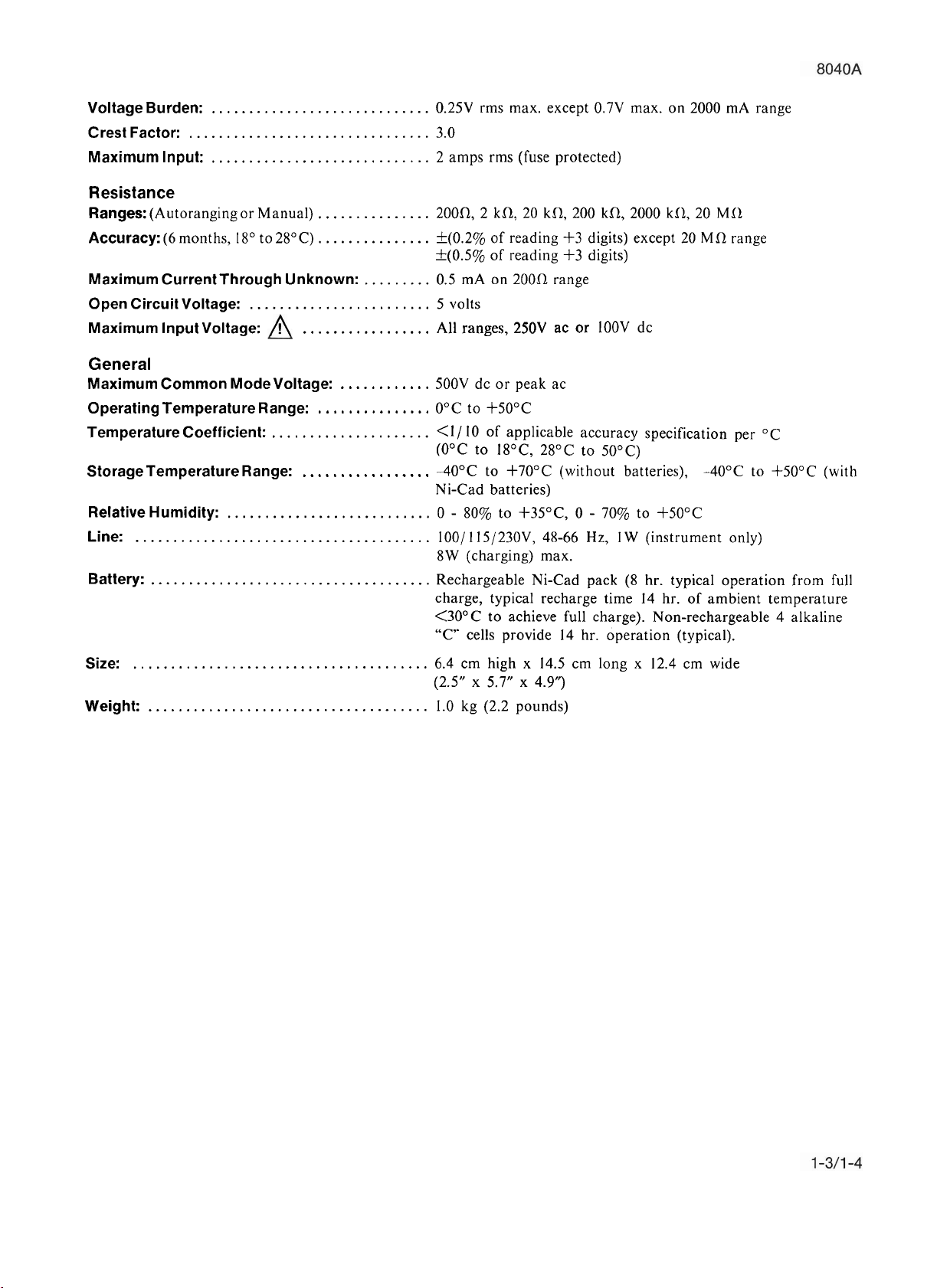
Control. Indicator and Connector Locations
Function Selection Examples
8040A Block Diagram
Simplified Buffer Circuit 3-3
Simplified
RMS Converter Representation 3-5
Simplified RMS Converter Circuit
Dual-Slope
Calibration Adjustment Controls 4-4
Required Method for Voltage Source Connection
Waveform at U26 Pin 8 for In Range and Overrange Inputs
Waveforms at TP1. Q10. C22 and U14 for In Range and Overrange Inputs
Oscilloscope Connections for Troubleshooting
A/ D Reference Circuit
A/ D Conversion Timing for VAC or VDC Inputs
.......................................................
.............................................................
...........................................................
....................................................
.....................................................
...................................................
....................................................
...........................................
............................
.......................................
...............................
..................
.........................................
PAGE
2-2
2-5
3-1
3-4
3-6
3-7
4-5
4-9
4-10
4-11
MainPCBAssembly ............................................................... 5-4
Digital Conditioner PCB Assembly
Analog Converter PCB Assembly
8040AAccessories
Initial
CaseTemperature above Ambient versus Meter Reading above Ambient
Maximum RF Signal Limits (V RMS) at Probe Tip
DeluxeTestLeadKit
801-600 Current Transformer
80F-5VoltageDivider
80F-
15 Voltage Divider
80K-40VoltageDivider
81RFHighFrequencyProbe
82RF High Frequency Probe
.................................................................
..............................................................
........................................................
.............................................................
............................................................
............................................................
........................................................
.........................................................
..................................................
....................................................
..................................... 6-4
iii
..............
5-8
5-10
6-2
6-4
6-4
6-5
6-5
6-6
6-7
6-7
6-7
Page 6
List
TABLE TITLE PAGE
of
Tables
Accessories
Control. Indicator and Connector Description
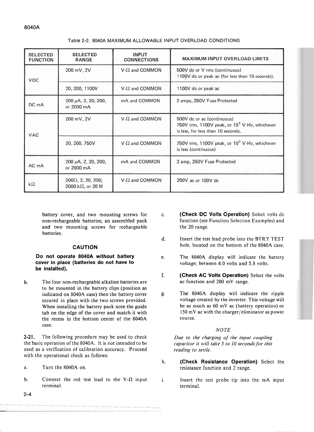
8040A Maximum Allowable Input Overload Conditions
Buffer Gain Configuration.
Recommended Test Equipment
DCVoltage
AC Voltage Performance Check 4-3
Resistance Performance Check
Direct Current Performance Check
DC Voltage Calibration
Ohms Calibration
LowFrequencyACVCheck
HighFrequencyACVCheck
Direct Current Accuracy Check
Battery
......................................................................
.........................................
.................................
kR Function
..............................................
......................................................
......................................................................
.....................................................
......................................................
...................................................
............................................................
.................................................................
........................................................
........................................................
......................................................
Charger/ Eliminator Input Power Configurations
................................
1 . 1
2-3
2-4
3-2
4-1
4-3
4-3
4-4
4-6
4-7
4-8
4-8
4-8
6-3
8040A Ranges for Current Transformer (801-600)
.......................................
6-5
Page 7
Section
1
Introduction
1-1. INTRODUCTION
1-2. The Model 8040A Multimeter provides the control applications.
accuracy and portability required in today's field service
work.
A
display from glare when operating the 8040A in adverse
lighting conditions. The small size and battery power add
to the portability; yet the fold-away stand allows the
instrument to be positioned at a convenient angle for
bench top use.
1-3.
five functions which provides measurement resolution to
0.01 ohms on the 200 ohm rangeand I0 microvolts on the Insure that the correct form of the model number is used
200 millivolt range.
The 8040A offers 20,000 count resolution in all temperature probe and A81 battery chargerleliminator,
sunshade
AC
protects
voltage and current measure- when ordering either of these accessories.
the
41/2
digit
LED
ments are made using true rms conversion techniques for
improved accuracy in communications and industrial
1-4. Several
8040A to expand its' capabilities. A list of these
accessories is provided in Table 1-1 while more detail
about
1-5.
are configured at the factory for particular applications.
&
each
Note that two of the accessories, the 80T-150
Specifications
accessories
one
is
provided
are
available
in
Section
6.
for
use
with the
ACCESSORY
801 -600
80F-5
8OF-15
80K-40
81
RF
82R
F
~OT-I~OC
80T-150F
C88
A80
8040A-
7004K
Table
DESCRIPTION
Clamp-on current probe; 2 to 600 amps
High voltage probe; 5
High voltage probe; 15 kV
High voltage probe; 40 kV
High frequency probe; 20 kHz to
100 MHz
High frequency probe;
500 MHz
Temperature probe;
-58'
F
to
+302'
Carrying case
Deluxe test lead kit
A battery cover kit; includes 4
size alkaline batteries
kV
100 kHz to
-50'~ to
F
+I
50'~
"C"
1-1.
ACCESSORIES
ACCESSORY
8040A7005K
8040A7007
K
A81-115
A81 -1 00
~81-230-~
A81-230
DESCRIPTION
A rechargeable Ni-Cad battery pack
(batteries come secured in the battery
cover)
A battery cover intended for use with
alkaline batteries (batteries not included:
Battery
50
Battery
50 to 60 Hz line source
Battery chargerleliminator for 230V,
50 to 60 Hz line source
plug)
Battery chargerleliminator for 230V,
50 to 60 Hz line source (European
type plug)
chargerleliminator for 11 5V,
to
60 Hz line source
charger/eliminator for IOOV,
(U.S.
type
Page 8
1-6.
DC Voltage
Ranges:
Accuracy:
Input Impedance:
Normal Mode Noise Rejection:
Common Mode Noise Rejection:
Maximum Input Voltage:
SPECIFICATIONS
(Autorangingor Manual)
(6 months, 18" to 28°C)
200 mV range:
1
2V thru
lOOV ranges:
..............
..............................
........................
............................
................
..............
.....................
A
AC Voltage (True rms)
Ratiges:
Accuracy:
Input Impedance:
Common Mode Noise Rejection:
Crest Factor:
Maximum Input Voltage: .....................
(Autoranging or Manual)
(6 months, 18' to 28OC, from 5% of
range to full range)
45 Hzto 10 kHz
10 Hz to 20 kHz
.............................
.............................
............................
................................
...............
..............
A
31200 mV, *2V, f20V, f 200V, f I
+(0.05% of reading f 3 digits)
f(0.05% of reading
10
MR,
all ranges
Greater than 60 dB at 50 Hz and 60 Hz
Greater than 120 dB at 50 Hz and 60 Hz
(1 kR in either lead)
200 mV and 2V ranges:
500V dc or rms ac (continuous)
1
IOOV dc or peak ac for less than 10 sec.
20V, 200V and 1 IOOV ranges:
1
IOOV dc or peak ac (continuous)
200 mV, 2V, 20V, 200V, 750V
+(0.5% of reading +I0 digits)
f
(1.0% of reading +I0 digits)
10 MR in parallel with less than 100 pF
Greater than 60 dB at 50 Hz and 60 Hz
(1
kR
in either lead)
3.0
200 mV and 2V ranges:
500V rms or 700V peak ac (continuous)
750V rms,
less than 10
20V, 200V and 750V ranges:
750V rms, 1 IOOV peak ac or
1100V peak ac or lo7 volt-hertz (whichever is less), for
sec.
+
2
digits)
IOOV
lo7
volt-hertz (whichever is less)
DC mA
Ranges:
Accuracy:
Voltage Burden:
Maximum Input:
AC Current (True rms, ac + dc)
Ranges:
Accuracy:
range to full range)
200
45 Hz to 20 kHz
2000 mA range:
45 Hz to 3 kHz
....................................
(6 months, 18" to 28°C)
...............
.............................
.............................
....................................
(6 months, 18" to 28"C, from 5% of
pA, 2 mA, 20 mA and 200 mA ranges:
...........................
..............................
+200 PA, 2 mA, 20 mA, 200
-t(0.3% of reading +3 digits)
0.25V rms max. except 0.7V rms max. on 2000 mA range
2 amps (fuse protected)
200 pA,2 mA,20 mA,200 mA,2000 mA
f
(1.0% of reading +lo digits)
+(1.0% of reading +10 digits)
mA,
2000 mA
,
Page 9
Voltage Burden:
Crest Factor:
Maximum Input:
Resistance
Ranges:(AutorangingorManual).
Accuracy:
Maximum CurrentThrough Unknown:
Open Circuit Voltage:
Maximum Inputvoltage:
General
Maximum Common Modevoltage:
Operating Temperature Range:
Temperature Coefficient:
StorageTemperatureRange:
Relative Humidity:
Line:
Battery:
(6 months, 18" to 28°C)
.......................................
.....................................
.............................
................................
.............................
..............
...............
........................
.................
............
...............
.....................
.................
...........................
.........
0.25V rms max. except 0.7V max. on 2000 mA range
3.0
2 amps rms (fuse protected)
2000, 2 kn, 20 k0, 200 k0, 2000 kfl, 20 Mf2
f
(0.2% of reading +3 digits) except 20 M0 range
f
(0.5% of reading +3 digits)
0.5 mA on 200n range
5 volts
All ranges, 25OV ac or IOOV dc
500V dc or peak ac
0°C to +50°C
<I 1 10 of applicable accuracy specification per
(0°C to 18"C, 28°C to 50°C)
-40°C to +70°C (without batteries), -40°C to +50°C (with
Ni-Cad batteries)
0 - 80% to +35"C, 0 - 70% to +50°C
1001 115/230V, 48-66
8W (charging) max.
Rechargeable Ni-Cad pack
charge, typical recharge time 14 hr. of ambient temperature
<30°C to achieve full charge). Non-rechargeable 4 alkaline
"C" cells provide 14 hr. operation (typical).
Hz,
I W (instrument only)
(8
hr. typical operation from full
oc
Size:
Weight:
.......................................
.....................................
6.4 cm high x 14.5 cm long x 12.4 cm wide
(2.5" x 5.7" x
1.0 kg (2.2 pounds)
4.9")
Page 10
Section
2
2-1. INTRODUCTION
2-2.
regarding the correct operation of the Model
Multimeter. It is recommended that the contents of this
section be read and understood before attempting to
operate the instrument. Should any difficulties arise
during operation, please contact your nearest John Fluke
Sales Representative, or the John Fluke Mfg. Co., Inc.,
P.O. Box 43210 Mountlake Terrace WA, 98043,
Telephone (206) 774-221
is located at the back of this manual.
2-3. SHIPPING INFORMATION
2-4. The 8040A was packed and shipped in a foam
container especially designed to provide adequate
protection. Upon receipt, inspect the instrument for
possible shipping damage.
2-5. If reshipment of the instrument is necessary, the
original container should be used. If the original
container is not available, a new one can be obtained
from the John Fluke Mfg. Co., Inc. Please reference the
instrument model number when requesting a new
shipping container.
2-6. INPUT POWER
2-7. Operating power for the standard 8040A
instrument comes from four, non-rechargeable, alkaline
"C"
hours of instrument operation. Optionally available
power sources include rechargeable Ni-Cad batteries and
a battery
with rechargeable batteries will typically operate for 8
hours; recharging, using the
approximately
This section of the manual contains information
8040A
I. A list of sales representatives
size batteries. The power source typically provides 14
charger/eliminator. The instrument equipped
charger/eliminator, takes
14
hours with the instrument turned off.
Operating
2-8. OPERATING FEATURES
2-9.
and connectors is shown in Figure 2-1. A description of
the control, indicator, or connector is provided in Table
2-1.
2-10. OPERATING NOTES
2-11. The following paragraphs describe various
conditions which should be considered before operating
the
2-12. Fuse Replacement
2-13.
fuse to protect the instrument circuitry from inadvertent
applications of current in excess of 2 amps. This fuse is
located behind the
pressing in lightly on the jack then turning it
counterclockwise
is necessary, use a
2-14. Overrange Indication
2-15. When the full scale capability of the selected
range for any function is exceeded, the display will blink.
The overrange indication does not necessarily mean that
the instrument is being exposed to a damaging input
condition.
2-16. Input Overload Protection
The location of the 8040A controls, indicators,
8040A.
The 8040A is equipped with a current overload
Exceeding the maximum input overload
conditions can damage the
Tables
the instrument.
2-2
l
nst ructions
rnA input jack and is removed by
1/4
turn to release. When replacement
2
amp
AGX
replacement fuse.
CAUTION
8040A.
before attempting to operate
Read
Page 11
1
2
8
LEFT SlDE
RIGHT SlDE
2-2
Figure
12
2-1.
CONTROL, INDICATOR AND CONNECTOR LOCATIONS
11
10
9
Page 12
Table
2-1.
CONTROL, INDICATOR AND CONNECTOR DESCRIPTION
8040A
ITEM
NUMBER
1
2
3
4
5
6
7
NAME
POWER switch
Display
Range switches
ka
V
mA
YY
AC
-
---
DC
DESCRIPTION
Separates the power source (batteries or battery eliminator) from
8040A circuitry.
A 4% digit display (19999 maximum) of the measured input,
including decimal point and polarity sign when appropriate.
The units annunicators
applicable range
Provide pushbutton selection of one of five ranges for each
function,
DC Voltage: 200 mV, 2,20,200,1 IOOV, or AUTO
AC Voltage: 200
AC or DC Current: 200
Resistance: 200s2, 2,20,200,2000 ka, or 20 M8IAUTO
Selects resistance measurement mode of operation.
Works in conjunction with the DC and AC switches to select the
voltage function (out position) or current function (in position).
This switch, in conjunction with item 5, selects ac voltage or
alternating current measurement capability.
This switch, in conjunction with item
direct current measurement capability.
i.e.,
(Ma or FA. mV 8) light when the
is
selected.
mV, 2,20,200,750V rms, or AUTO
PA, 2,20,200, or 2000 mA
5,
selects dc voltage or
8
10
11
12
BATTERY CHARGER/
ELIMINATOR
9
V-s2
COMMON
m
A
Sunshade
Jack provided for connection of the chargerleliminator
accessory.
Jack for high (red) lead connection to
and resistance measurements.
Jack for low (black) lead connection to
Jack for high (red) lead
measurements (2A FUSE behind; push in and twist
to remove).
Shade slides forward to improve the readability of the displays in
bright light environments.
2-17. The overload protection varies with the range
and function selected. The maximum allowable input
overload condition for each function and range is given in
r able
2-2.
2-18.
ASSEMBLY AND INITIAL OPERATION
2-19. It is recommended that the assembly and initial
operation of the
8040A be done in accordance with the
following procedure. No test equipment is required to
8040A for voltage (ac or dc)
8040A for all functions.
conrlection to 8040A for current (ac and dc)
'/4
turn and pull
perform this procedure; all signals observed are generated by the
instrument operational evaluation when the
8040A. This procedure may be used as an
8040A is
being used in locations away from normal calibration
equipment.
2-20. Assemble the 8040A as follows:
a. Remove the contents of the box marked
BATTERY COVER. (Four
"C" size batteries, a
Page 13
8040A
Table
2-2.
8040A MAXIMUM ALLOWABLE INPUT OVERLOAD CONDITIONS
battery cover, and two mounting screws for
non-rechargeable batteries; an assembled pack
and two mounting screws for rechargeable
batteries.
CAUTION
Do not operate
8040A
without battery
cover in place (batteries do not have to
be installed).
b.
The four non-rechargeable alkaline batteries are
to be mounted in the battery clips (position as
indicated on
8040A case) then the battery cover
secured in place with the two screws provided.
When installing the battery pack note the guide
tab on the edge of the cover and match it with
the recess in the bottom center of the
8040A
case.
2-21.
the basic operation of the
The following procedure may be used to check
8040A. It is not intended to be
used as a verification of calibration accuracy. Proceed
with the operational check as follows:
a. Turn the 8040A on.
c.
(Check DC Volts Operation)
Select volts dc
function (see Function Selection Examples) and
the 20 range.
d.
Insert the test lead probe into the
BTRY
TEST
hole, located on the bottom of the 8040A case.
e. The 8040A display will indicate the battery
voltage; between 4.0 volts and 5.8 volts.
f.
(Check
AC
Volts Operation)
Select the volts
ac function and 200 mV range.
€5 The 8040A display will indicate the ripple
voltage created by the inverter. This voltage will
be as much as 60
mV ac (battery operation) or
150 mV ac with the charger/eliminator as power
source.
NOTE
Due to the charging oJ the inpur c~oupling
capacitor it will take 5 to
I
reading
h.
o settle.
(Check Resistance Operation)
10
secondsfbr this
Select the
resistance function and 2 range.
b. Connect the red test lead to the V-0 input
terminal.
I.
Insert the test probe tip into the mA input
terminal.
Page 14
j.
k.
The 8040A display will indicate 0.100
(Check
test lead to the
DC
mA Operation)
mA input terminal.
+2
Connect the red
1. Select the dc mA function and 2 range.
digits.
0.
P.
(Check AC mA Operation)
Select the ac mA
function.
The 8040A display will indicate the same as step
n
(mA input is dc coupled).
m. Place the test probe tip into the BTRY TEST
2-22.
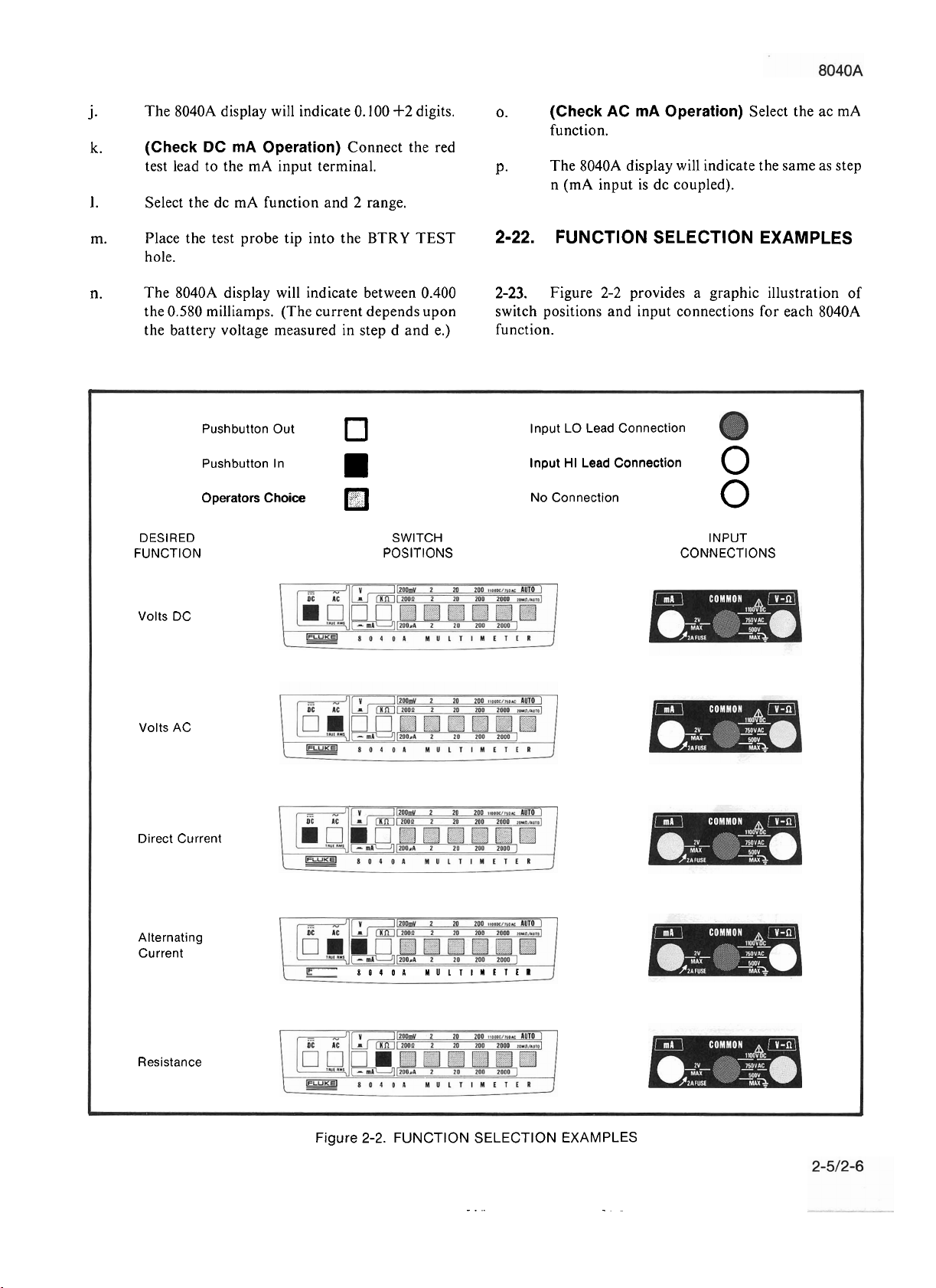
FUNCTION SELECTION EXAMPLES
hole.
n. The 8040A display will indicate between 0.400
the 0.580
milliamps. (The current depends upon
the battery voltage measured in step d and e.)
Pushbutton Out Input LO Lead Connection
Pushbutton In
Operators Cho~ce
DESIRED SWITCH INPUT
FUNCTION POSITIONS CONNECTIONS
Volts DC
2-23.
switch positions and input connections for each
function.
Figure
Input HI Lead Connection
NO
Connection
2-2
provides a graphic illustration of
8040A
0
O
Volts AC
D~rect Current
Alternating
Current
Res~stance
Figure
80401
2-2.
MULTIMCTCR
FUNCTION SELECTION EXAMPLES
-.
.
-
Page 15
Section
3
3-1.
3-2.
arranged under two major headings. The first, titled
OVERALL FUNCTIONAL DESCRIPTION, discusses
the overall operation of the instrument in terms of the
functional relationships of the major circuits. The
second section is titled CIRCUIT DESCRIPTION and
deals with the internal operation of each major circuit in
more detail. Block diagrams and simplified circuit
diagrams are included, where needed, to aid in
understanding the theory. The complete schematic
diagrams are located in Section
INTRODUCTION
The theory of operation for the Model 8040A is
7.
-
-
-
-
-
-
-
-
-
- - -
v-n
I
I
I
I
I
I
INPUT
DIVIDER
ANALOG
I
I
OHMS
VOLTAGE
SOURCE
I
I
SHUNTS
SUPPLIES
-
Theory
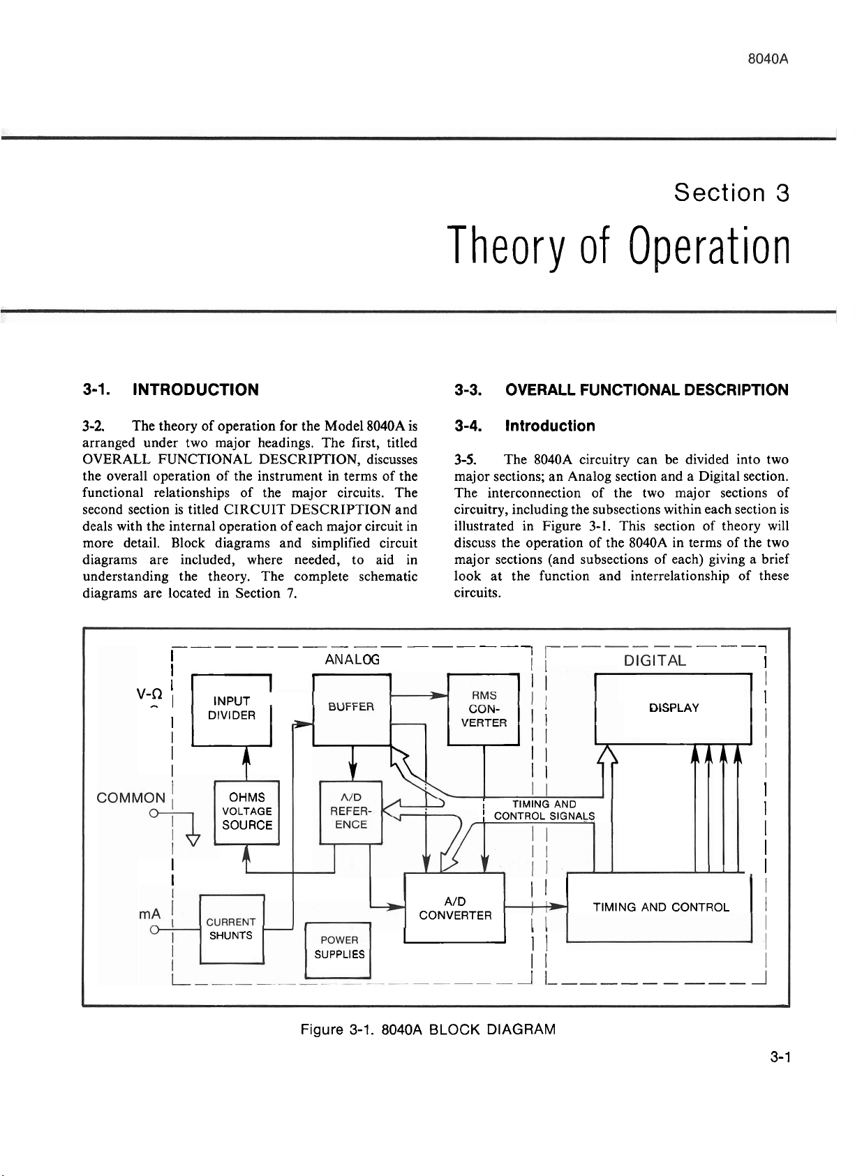
3-3.
3-4.
3-5.
major sections; an Analog section and a Digital section.
The interconnection of the two major sections of
circuitry, including the subsections within each section is
illustrated in Figure
discuss the operation of the
major sections (and subsections of each) giving a brief
look at the function and interrelationship of these
circuits.
-
OVERALL FUNCTIONAL DESCRIPTION
Introduction
The 8040A circuitry can be divided into two
-
-
1
of
Operation
3-1.
This section of theory will
8040A in terms of the two
---
DISPLAY
A
i
TIMING AND
I
CONTROL SIGNALS
A/D
CONVERTER
I I
II
I
I
I
I
TIMING AND CONTROL
A
1
I
I
I
I
I
I
I
I
I
I
I
I
I
I
I
1
Figure
3-1.
8040A
BLOCK
DIAGRAM
3-
1
Page 16
3-6. Analog Circuits
3-7. The Analog portion of the 8040A circuitry
consists of an Input Divider, Buffer, RMS Converter,
Ohms Voltage Source, A/ D Reference, Current Shunts,
Power Supplies and
measured are connected to the Analog circuitry via the
V-R or
proportional to the applied input, is developed by the
Input Divider, Current Shunts, Buffer and RMS
Converter and applied to the
voltage equivalent of the applied input charges a
capacitor in the
input. A reference voltage, opposite in polarity to the
voltage representing the applied input, is then connected
to the
at a constant rate. The time it takes the capacitor to
discharge is therefore proportional to the applied input.
the Digital section of
and displays it as a digital representation of the input
circuit.
mA terminals. A dc voltage, directly
A/D causing the charged capacitor to discharge
A/D Converter. The inputs to be
A/D Converter. This dc
AID to a level proportional to the
8040A circuitry measures the time
3-8. Digital Circuits
3-9. The Digital section consists of Timing and
Control and Display circuits. The Timing and Control
Signals connect the dc voltage representing the input
being measured to the A/ D for 100 ms then disconnect
it and apply the reference voltage. At the time the
reference voltage is applied the Timing and Control
circuit starts counting the number of cycles of the
Crystal Oscillator occur until the A/ D sends a signal to
the Timing and Control circuit indicating that the
capacitor has been discharged to zero. The number of
cycles of oscillator signal that occurred is presented on
the display as the value of the unknown input being
measured by the
8040A.
be connected in series with the unknown resistance
applied to the
The Ohms Source Voltage is applied to this voltage
divider and the voltage drop across the unknown
resistance is measured by the
value of the resistance.
V-R terminal to form a voltage divider.
8040A to calculate the
3-15. Current Shunts
3-16. The Current Shunts are a set of series connected
resistors. The unknown current applied to the mA
terminal develops a voltage proportional to the
current, across the portion of the shunt resistors selected
by the range switch. The
developed across the shunt resistor and displays the
value of the input current.
8040A processes the voltage
3-17. Buffer
3-18.
(measurement of dc or ac volts), the
(measurement of resistance) or the Current Shunts
(measurement of dc or ac
Buffer (see Figure 3-2). The gain of the Buffer is changed
to compensate for the changes in the output voltage of
the Input Divider and Current Shunts. A combination
of buffer gain
Divider or Current Shunts is selected so that the output
of the Buffer will not exceed 2V dc (or rms) for any full
scale input in either the dc (or ac) voltage or current
function. Because of changes in the reference voltage
used in the resistance function (explained in the
Reference theory) the output of the Buffer, for full scale
inputs, changes when the range changes. Table 3-1
provides the gain and Buffer output information for
each range.
The output voltage of either the Input Divider
V-R terminal
mA) is applied to 48 in the
(XI or X10) and scale factor of the Input
A/D
3-10. CIRCUIT DESCRIPTION
3-11. Introduction
3-12.
look at the subsections of circuitry, as presented in the
block diagram, in more detail. When needed for
explanation, simplified schematic diagrams of the
circuits being discussed will be provided.
This section of 8040A theory of operation will
3-13. Input Divider
3-14. The Input Divider performs two basic functions
when measuring unknown inputs applied to the
terminal. First, when measuring either dc or ac voltages,
the divider is used to scale the input voltages down to a
level that can be handled by the Buffer. The second
function of the divider is to provide resistors which can
V-R
Table
-
3-1.
RANGE
200
2
kfi
20
kfi
200
ka
2000
kc2
20 Ma
BUFFER GAlN CONFIGURATION,
kn
FUNCTION
BUFFER GAIN
AND DIVISION
XIO,
+
XIO,
+
XI,
+
1
XIO,
+
XI,
+I
XI, +I0
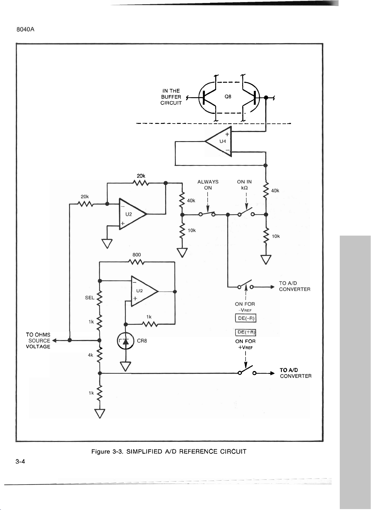
3-19. AID Reference
3-20.
to the
After the output of the Buffer has been applied
A/
D Converter for 100 ms the timing and control
1
I
I
FULL SCALE
BUFFER OUTPUT
980 mV
980 mV
833 mV
980 mV
833 rnV
333 mV
Page 17
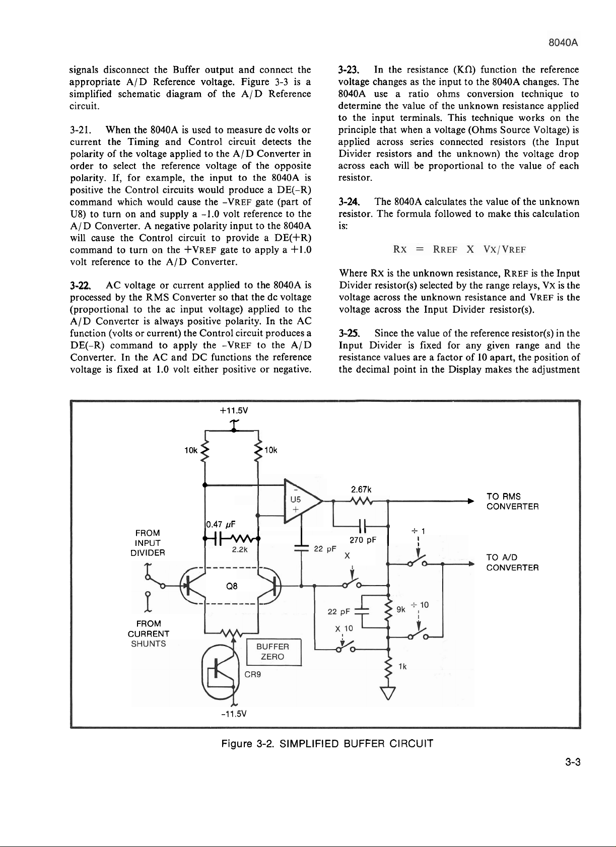
signals disconnect the Buffer output and connect the
appropriate
simplified schematic diagram of the
circuit.
3-21.
current the Timing and Control circuit detects the
polarity of the voltage applied to the A/
order to select the reference voltage of the opposite
polarity. If, for example, the input to the
positive the Control circuits would produce a
command which would cause the -VREF gate (part of
U8) to turn on and supply a -1.0 volt reference to the
A/ D Converter. A negative polarity input to the
will cause the Control circuit to provide a DE(+R)
command to turn on the +VREF gate to apply a 4-1.0
volt reference to the A/D Converter.
3-22.
processed by the RMS Converter so that the dc voltage
(proportional to the ac input voltage) applied to the
A/D Converter is always positive polarity. In the AC
function (volts or current) the Control circuit produces a
DE(-R) command to apply the -VREF to the A/D
Converter. In the AC and DC functions the reference
voltage is fixed at 1.0 volt either positive or negative.
A/D Reference voltage. Figure 3-3 is a
AID Reference
When the 8040A is used to measure dc volts or
D
Converter in
8040A is
DE(-R)
8040A
AC voltage or current applied to the 8040A is
3-23.
voltage changes as the input to the
8040A use a ratio ohms conversion technique to
determine the value of the unknown resistance applied
to the input terminals. This technique works on the
principle that when a voltage (Ohms Source Voltage) is
applied across series connected resistors (the Input
Divider resistors and the unknown) the voltage drop
across each will be proportional to the value of each
resistor.
3-24. The 8040A calculates the value of the unknown
resistor. The formula followed to make this calculation
is:
Where RX is the unknown resistance, RREF is the Input
Divider
voltage across the unknown resistance and VREF is the
voltage across the Input Divider
3-25.
Input Divider is fixed for any given range and the
resistance values are a factor of 10 apart, the position of
the decimal point in the Display makes the adjustment
In the resistance
resistor(s) selected by the range relays, Vx is the
Since the value of the reference resistor(s) in the
(KR)
function the reference
8040A changes. The
resistor(s).
+11.5v
T
10k 10k
41
0.47 pF
FROM
INPUT 270 pF
DIVIDER
Q8
FROM
CURRENT
2.67k
+
.
TO
RMS
CONVERTER
1
TO
A/D
CONVERTER
-1 1.5V
Figure
3-2.
SIMPLIFIED BUFFER CIRCUIT
3-3
Page 18
IN
THE
BUFFER
CIRCUIT
f++!!-ii
-
---
-)-
-
---------
20k
---------------
----
-
3-4
TO OHMS
VOLTAGE
Figure
3-3.
SlMPLl
FlED
A/D
REFERENCE CIRCUIT
ON FOR
+VREF
I
I
v
d-
TO
A/D
CONVERTER
Page 19
for the RREF term in the formula. The 8040A directly
reads the value of
output to the
VREF is determined by algebraically adding
positive voltage) to a negative equivalent of the ohms
source voltage. The resulting voltage is VREF and is
applied to the
application of
Vx and applies the resulting Buffer
AID Converter for 100 ms. The value of
VX (a
A/D Converter at the end of the 100 ms
Vx.
3-31.
~ulti~lier-Divider function is performed using a LogAntilog circuit. The base-emitter voltage of a transistor
is almost perfectly logarithmically related to the
collector current.
obtain two times the log of the input; then by taking the
antilog we obtain a voltage proportional to the square of
the input
In the 8040A implicit conversion method the
By
putting two transistors in series we
(Vi2).
3-26.
3-27.
positive voltage source in the
ational amplifier
schematics in Section 7) make up the unity gain buffer
amplifier that supplies the ohms source voltage. The
Ohms Voltage Source circuit is used exclusively in the
resistance measurement function.
3-28.
3-29. An rrns amplitude is that value of alternating
current or voltage that results in the same power
dissipation in a given resistance as dc current or voltage
of the same numerical value. The mathematical formula
for determining the rms value of an ac voltage is:
Where Vi is the value of the ac voltage at any given
instant. The
instantaneous voltage and computes the rrns value of the
input signal.
3-30. The 8040A uses an implicit method for
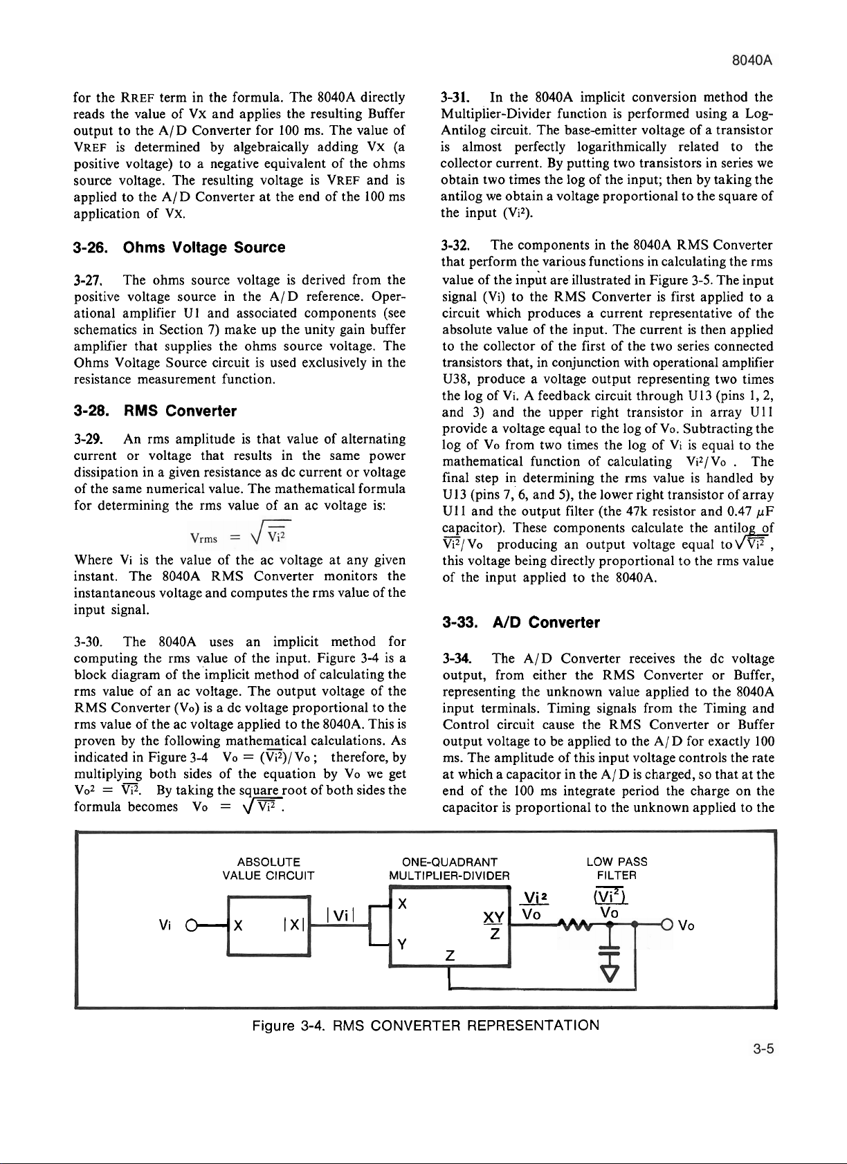
computing the rrns value of the input. Figure 3-4 is a
block diagram of
rms value of an ac voltage. The output voltage of the
RMS Converter (VO) is a dc voltage proportional to the
rrns value of the ac voltage applied to the
proven by the following mathematical calculations. As
indicated in Figure 3-4 Vo
multiplying both sides of the equation by Vo we get
Vo2
formula becomes Vo
Ohms
The ohms source voltage is derived from the
Voltage Source
AID reference. Oper-
U1 and associated components (see
RMS Converter
8040A RMS Converter monitors the
the'implicit method of calculating the
8040A. This is
=
(K)/VO ; therefore, by
=
Vi2. By taking the square root of both sides the
=
m.
3-32. The components in the 8040A RMS Converter
that perform the various functions in calculating the rrns
value of the
signal (Vi) to the RMS Converter is first applied to a
circuit which produces a current representative of the
absolute value of the input. The current is then applied
to the collector of the first of the two series connected
transistors that, in conjunction with operational amplifier
U38, produce a voltage output representing two times
the log of Vi. A feedback circuit through U 13 (pins
and 3) and the upper right transistor in array U11
provide a voltage equal to the log of Vo. Subtracting the
log of Vo from two times the log of Vi is equal to the
mathematical function of calculating
final step in determining the rrns value is handled by
U13 (pins
U11 and the output filter (the 47k resistor and 0.47
capacitor). These components calculate the antilo of
V/VO
this voltage being directly proportional to the rms value
of the input applied to the
3-33.
3-34. The AID Converter receives the dc voltage
output, from either the RMS Converter or Buffer,
representing the unknown value applied to the
input terminals. Timing signals from the Timing and
Control circuit cause the RMS Converter or Buffer
output voltage to be applied to the
ms. The amplitude of this input voltage controls the rate
at which a capacitor in the
end of the 100 ms integrate period the charge on the
capacitor is proportional to the unknown applied to the
inpit are illustrated in Figure 3-5. The input
Vi2/Vo . The
7,6,
and
5),
the lower right transistor of array
producing an output voltage equal to&,
8040A.
AID
Converter
A/ D for exactly 100
A/D is charged, so that at the
1,2,
pF
8040A
Vi
O---X
ABSOLUTE
VALUE
CIRCUIT
I
XI
I
Vi
I
ONE-QUADRANT
MULTIPLIER-DIVIDER
-
X
-
Y
XY
z
3
Vi2
-
VO
z
I
Figure 3-4. RMS CONVERTER REPRESENTATION
LOW
FILTER
-
(vi2)
vo
PASS
vo
b
Page 20

8040A. At the end of the 100 ms integrate period the
input to the
AID is then connected to the AID
Reference. The reference voltage is selected, by the
Timing and Control circuit, to be opposite in polarity
from the output of the Buffer or RMS Converter. The
reference voltage causes the capacitor in the
AID
Converter to discharge at a constant rate. The time,
called read period, that it takes the capacitor to
discharge is directly proportional to the unknown input
applied to the
8040A. Figure
3-6
illustrates the charge-
discharge cycle of the A/D capacitor for ac or dc volts
or current inputs. The charge-discharge cycle of the
A/ D capacitor in the
Ki2
function is unique because the
reference voltage is inversely related to the unknown
resistance value. This causes the discharge rate (slope)
during the read period to change with the input.
3-35. Timing and Control
3-36.
with the
an analog representation of the unknown input into a
digital representation. Signals from the Timing and
Control circuit select the Buffer gain and the signal path
for processing the unknown input. Correct timing of
these signals is derived from a 1
oscillator.
The Timing and Control circuit, in conjunction
A/D Converter output, change what has been
MHz
crystal controlled
3-37.
All of the digitizing process (the actual counting
of the oscillator pulses during the read period) takes
place in the custom integrated circuit
U25.
The pulses
accumulate, during the read period, in decade counters
within the custom chip. The number in each decade
counter is converted to a four-bit binary code. Strobe
signals, generaed by the custom chip, then cause the
binary code for one decade counter at a time to be sent
to the Display circuitry where the same strobe signal
causes one of the LEDs of the display to be
to display
that number.
strobed on
3-38. Display
3-39.
through ST7) some of which are used by the Display
circuits to turn on the LEDs one at a time. The four-bit
binary coded digit information applied to the Display is
first changed, by
the binary code to seven driver signals; one for each
segment in the LEDs. The seven segment drive signals
are connected in parallel to each of the display digits.
The strobe signals allow only one display LED to light
at a time. The strobe signal causes the digit in the display
corresponding to the digit with the same significant
value transmitted from the Timing and Control circuit
to appear in the correct position.
The custom chip provides strobe signals
U27
(see schematic in Section
7),
(ST@
from
20k
I
I
I
I
I
I CIRCUIT
I
I
ABSOLUTE VALUE
VOLTAGE-TO-CURRENT
Figure
I
I
I
I
I
I
3-5.
SIMPLIFIED RMS
2
X
LOG
OR
SQUARING
CIRCUIT
I
I
LOG FEEDBACK
I
CIRCUIT
I
I
CONVERTER
I
I
I
I I
CIRCUIT
40k
AND OUTPUT
FILTER
CIRCUIT
,
1
FILTER
1
I
I
I
Page 21

AID INTEGRATOR
OUTPUT VOLTAGE
CLOCK
OSCILLATOR
SIGNAL
INTEGRATE PERIOD
SLOPE is proportional to the
instrument input signal
t
I
I
A
\
I
I
wL
100
ms READ PERIOD
TIME is proportional
the instrument, input
signal
t
I
ZERO
LEVEL
J
to
I
J
J
Figure
3-6.
DUAL-SLOPE AID CONVERSION TIMING FOR VAC OR VDC INPUTS
Page 22

Section
Maintenance
WARNING!
THESE SERVICING INSTRUCTIONS ARE FOR USE BY QUALIFIED PERSONNEL ONLY. TO
AVOID ELECTRIC SHOCK, DO NOT PERFORM ANY SERVICING OTHER THAN THAT
CONTAINED IN THE OPERATING INSTRUCTIONS UNLESS YOU ARE QUALIFIED TO DO SO.
4
4-1,
4-2.
on service, general maintenance, performance tests,
calibration, and troubleshooting. The performance test
is recommended as a preventative maintenance tool, and necessary to maintain the
should be executed when it is necessary to verify that the equipment is not available, other equipment having
instrument is operating within the specification limits.
INTRODUCTION
This section of the manual contains information
Table 4-1. RECOMMENDED
NOMENCLATURE
AC Calibrator
DC Calibrator
DC Current
Cali brator
Voltage Range: 0 to 750V ac
Frequency Range: 45
Voltage Accuracy: 45 Hz to
Voltage Range: 0 to 1 100V dc
Accuracy:
Current Range:
Accuracy: 0.03%
MINIMUM
calibration interval of 6 months is recommended to
insure that the
stated in Section 1.
A
4-3.
equivalent specifications may be used.
Table 4-1 lists the recommended test equipment
TEST
USE SPECIFICATIONS
Hz
to 120 kHz
10 kHz .
10kHzto120kHz
-
+
0.005%
0 to 2 mA
8040A
performs within the specifications
EQUIPMENT
.
.
. . 0.1%
.
. .
.
0.2%
8040A.
If the specified
RECOMMENDED
EQUIPMENT
John Fluke
Model
and 5205A
John Fluke
Model 33308
John Fluke
Model 33308
5200A
DC Current
brator
Cali
Digital Multimeter
Resistor Decade
Oscilloscope
Counter
2
-
mA to 2A
0.03%
%
Current Range:
Accuracy:
DC Voltage Accuracy: 0.1
Resistance Accuracy: 20.04%
General Purpose with 10 Mi2 probe
-
+25 ppm at 1 MHz
John Fluke
Model 382A
John Fluke
Model 8040A
ESI DB62
Tektronix 465
John Fluke
Model 1900A
Page 23

4-4. GENERAL MAINTENANCE
4-5. Access Information
4-6.
the interior of the 8040A:
1.
Use the following procedure to gain access to
Set the POWER switch to OFF and disconnect
the battery charger eliminator, if attached.
9.
10. The A4 pcb can be removed with upward
Remove the circuit shield covering the A4
(Input) pcb and switches for inspection or
troubleshooting purposes. One screw holds it in
place.
pressure and a gentle rocking motion.
2.
3.
Remove the fuse from the mA jack (press in,
turn counterclockwise
Remove the two screws holding the battery
holder to the rear of the instrument and remove
the holder and batteries.
'/4
turn to release).
NOTE
The rechargeable batteries are secured to the
battery holder and are removed as one unit.
4.
Remove the screw from the center of the rear
panel of the instrument case and slide the
8040A out of the case.
NOTE
Do not attempt to remove the sunshade
when the
8040A
is in the case. The sunshade
does not have to be removed to slide the
instrument out
There are two wires connecting the
8040A circuitry to the battery contactors
in the case. Use care not to place
excessive strain on these wires.
of the case.
CAUTION
11. When reassembling the 8040A, protect the
flexible lands by first folding the switch section
of the
towards the vertical A2 and A3 pcbs. Tip the
bottom edge of the front panel up to clear the
switches. Insure that the A2 and A3 boards fit
into the plastic board edge retainers on each
side.
4-7. Cleaning
4-8.
alcohol or a mild solution of detergent and water. Clean
dust from the circuit board with low pressure dry air.
Contaminates can be washed from the circuit board
with demineralized water and a soft brush (avoid getting
excessive amounts of water on the switches).
4-9. Fuse Replacement
Clean the front panel and case with denatured
Do not use aromatic hydrocarbons or
chlorinated solvents for cleaning. These
solutions will react with the plastic
materials of the instrument.
A1 pcb then the display section up
CAUTION
5.
6.
7.
8.
Unplug the battery power wires from the 8040A
circuit board.
Loosen the two screws securing the circuit
board to the top of the front panel. DO NOT
REMOVE THEM!
Remove the two screws securing the circuit
board to the bottom of the front panel.
Set the 8040A, front panel up, on a flat surface
and gently lift the bottom edge of the front
panel up to clear the switch buttons. Gently lay
the switch and display sections of the
down on the flat surface.
CAUTION
Do not bend the circuit board backwards
past the flat position as damage to the
flex joints may occur.
A1 pcb
4-10. A fuse, located behind the mA input jack,
provides protection against current inputs that exceed 2
amps. When replacement is required, use only a AGX 2
amp fuse as a replacement. This fuse is removed by
pressing in on the
counterclockwise
4-11. PERFORMANCE CHECK
4-12.
verifying that the overall operation of the
within required limits. This procedure can be used as a
acceptance test for receiving inspection and as a periodic
maintenance -check. Refer to Table 4-1 for the test
equipment
8040A fail to meet the requirements of these checks
calibration and/or troubleshooting will be necessary.
See Table 4-1 for recommended calibration equipment.
Perform this procedure under environmental conditions
of 23
The performance check provides a means of
recodmended for these checks. Should the
f
5OC at relative humidity less than 80%.
mA input terminal then turning it
'/4
turn to release.
8040A is
Page 24

WARNING
REFER TO THE REQUIRED METHOD
FOR VOLTAGE SOURCE CONNECTION
(THIS SECTION) FOR VOLTAGE SOURCE
CONNECTION PROCEDURE.
4-14.
voltage source (see Table
be applied to the
This procedure requires the output of a dc
4-l), set to specified levels, to
8040A V-R and COMMON input
while the display is observed to be within specific limits.
Select the DC V function then refer to Table 4-2 for the
ranges and inputs for the performance check.
limits. Select the DC mA function then refer to Table
4-5 for the ranges and inputs for the current check.
4-21. Alternating Current
4-22.
not be checked because the accuracy of the shunts is
established by the direct current check and the
frequency response is determined by the ac converter
which is checked during the ac voltage check.
Table
The alternating current mode of operation need
4-3.
AC VOLTAGE PERFORMANCE CHECK
8040A
RANGE
ACVOLTS
INPUT
INPUT
FREQ
8040ADlSPLAY
LIMITS
Table
4-2.
DC VOLTAGE PERFORMANCE CHECK
8040A
RANGE
200 mV
2
2
20
20
200
200
1100
dc
1100
dc
DC VOLTS
INPUT
190.00 mV
1.900V
0.90V
19.00V
9.00V
190.00V
50.00V
10OO.OOV
450.00V
8040A DISPLAY
LIMITS
to
to
to
to
to
to
to
to
to
190.1 3
1.901 2
0.9007
19.012
9.007
190.12
50.05
1000.7
450.4
189.87
1.8988
0.8993
18.988
8.993
189.88
49.95
999.3
449.6
4-16. During this procedure ac voltage levels at
specified frequencies are applied to the
8040A V-R and
COMMON inputs and the displays observed to be
within'specific limits. Select the AC V function then
refer to Table
4-3
for the ranges and inputs for the
performance check.
4-17. Resistance Measurements
4-18.
be applied to the
the display observed to be within specified limits. Select
the
and inputs for the performance check.
This procedure calls for precision resistance to
8040A V-R and COMMON inputs and
KR function then refer to Table
4-4
for the ranges
4-19. Direct Current
4-20. This procedure calls for known values of direct
current to be applied to the
inputs and the display observed to be within specified
8040A mA and COMMON
200 mV
200 mV
200 mV
2
2
?
20
20
20
200
200
750
750
Table
8040A
RANGE
AUTO
AUTO
AUTO
2000 k!2
200i-L
AUTO
AUTO
AUTO
AUTO
AUTO
AUTO
1
190.0 mV
190.0 mV
190.0 mV
1.900V
0.900V
1.900V
19.00V
8.00V
19.00V
190.0V
190.0V
750V
750V
4-4.
RESISTANCE PERFORMANCE CHECK
RESISTANCE
INPUT
SHORT
SHORT
OPEN
1.0 Ma
1
OOn
1
.OO
5.00 ki-L
10.0 kc2
100 kc2
500 kQ
10.0
Use a good quality shorting bar between the
50Hz
5 kHz
20 kHz
50 Hz
10 kHz
20 kHz
50 Hz
5 kHz
20 kHz
50 Hz
20 kHz
50 Hz
13 kHz
@
@
kS1
MQ
188.95to191.05
188.95
188.00
1.8895
0.8945
1.8800
18.895
7.950
18.800
0.89405
188.00
745.2
741.5
8040A DISPLAY
00.00
Lead Res Value
Flashing
997.7
99.77
.9977
4.987
9.977
99.77
498.7
9.947
and COMMON-input terminals.
2
Connect the test leads that will be used to connect
the
8040A
to the decade resistance source. Place
the short at the end of the test leads that will be
connected to the resistance source. Note the
resistance value indicated on the
3
Add the lead resistance value to the input resistance
value to determine the correct
8040A
8040A
to
to
to
to
to
to
to
to
to
to
to
to
LIMITS
to
00.03
+I
.8888
to
1002.3
to
100.23
to
1.0023
to
5.013
to
10.023
to
100.23
to
501.3
to
10.058
display.
display.
191.05
192.00
1.91 05
0.9055
1.9200
19.1 05
8.050
19.200
0.9055
192.00
7.548
7.585
@
@
@
V-a
Page 25

4-4
Figure
4-1.
CALIBRATION ADJUSTMENT CONTROLS
Page 26

8040A
RANGE
Table
4-5.
DIRECT CURRENT
PERFORMANCE CHECK
DIRECT CURRENT
l
NPUT
8040A
LIMITS
ground connection will insure that voltage potential,
harmful to the calibration or repair technician, will not
be present on the instrument's common circuits.
DISPLAY
WARNING
+I
89.40
to
+I
200
pA
2
20
200
2000
+I
90.0
+I
.900
+I
9.00
+I
90.0
+I900
pA
mA
mA
mA
mA
+I
.8940
+18.940
+I
89.40
+1894.0
90.60
to
+I
.9060
to
+19.060
to
+I
90.60
to
+1906.0
NOTE
In the AC
mA function inputs to the 8040A
are dc coupled this aIIows this function to be
checked with a dc
mA input. Do t.his by
seIecting the AC mA function and 2 range.
+1.9
Apply
mA dc to the mA input. The
8040A display should read between 1.8800
and 1.9200.
4-23.
CALIBRATION
4-24. Calibration of the Model 8040A should be done
after repairs have been made to the electronic circuitry
or when the performance check indicates the unit is not
operating within the specification. Table 4-1 provides a
list of test equipment required to calibrate this
instrument. These procedures should be performed
under environmental conditions of 23
f
5OC at a relative
humidity of less than 80%.
Insure that the voltage source connection method illustrated in Figure
4-2
is used. Other connection methods may
cause hazardous voltages to be present
on the
8040A
common circuits.
DO NOT CONNECT
GROUND
GROUND AND OUTPUT
LINK BETWEEN
LOW
4-25.
It is recommended that the 8040A circuit board
remain folded up and attached to the front panel. All
adjustments and test points are accessible through the
open sides of the folded up unit. The location of each
calibration adjustment is illustrated in Figure 4-1. The
steps of this procedure must be performed in the order
presented.
NOTE
The physical position of some components
may affect the ac calibration of the
instrument. Avoid moving the components,
especially after the calibration procedure has
been completed.
4-26.
Required Method for Voltage Source
Connection
4-27.
When a DMM is opened for servicing, the
voltage source connections to it must be made in the
manner shown in Figure 4-2. This method is required
for PERSONAL SAFETY. Since a DMM has no earth
ground connection in itself, the earth ground connection
must be
suplied from the voltage source. The earth
Figure
4-28.
1.
4-2.
REQUIRED METHOD
SOURCE CONNECTION
FOR
VOLTAGE
Perform the 8040A calibration as follows:
On the
8040A
select the AC
mA
function and
range.
2.
3.
Connect the positive lead of the test equipment
voltmeter to TPI on the
to the
8040A COMMON input terminal.
8040A and the low lead
Adjust R42 for a voltmeter reading of -0.001 to
+0.001 volts.
\,
4. Disconnect the teht,equipment voltmeter.
5.
Select the DC V function.
2
Page 27

8040A
Table 4-6. DC VOLTAGE CALIBRATION
I
STEP
1
2
3
4
5
6
7
8
9
10
11
12
13
14
15
16
17
*
Reverse the polarity of the applied input
RANGE
200 mV
200 rnV
2
2
2
2
2
200
rnV
200 mV
Repeat steps 8 and 9 until the tolerance is equal
AUTO
AUTO
AUTO
AUTO
AUTO
AUTO
AUTO
INPUT
SHORT
OPEN
-1.9000V
+I
0.0000v
-1.9000V
-1.8000V
+I 90.00 mV
1
-190.00 mV
+190.00V
+I
+I
OPEN
+lOOO.OV
SHORT
-1OOO.OV"
.9000V
.9000V
9.000V
ADJUST
-
-
R31
R38
-
-
-
R60
1
R60
R
-
-
-
R3
-
-
(1000
9
volts) by decreasing the voltage source output to zero, inverting the
8040A
DISPLAY
00.00
00.00
-1
+I
.oooo
-1 .go00
-1.8000
+I
1
-190.00
in
+I
+I
+I
00.00
+1000.0
00.00
-1 000.0
.go00
.go00
90.00
each polarity.
90.00
.go00
9.000
output lead at the voltage source output jacks, then increase the voltage to
Voltage Source Connection).
i
ANNUNCIATOR
mV
L!
mV
L!
-
-
-
-
rnV
L!
1
mV
L!
-
-
-
rnV
L!
-
rnV
C?
-
1000
volts (see Required Method for
pA
pA
pA
pA
pA
pA
TOLERANCE
-00.02
-01
exactly
exactly
-.0002
-1.8998
-1.7998
+189.98
1
-189.98
exactly
+I
.8998
+18.998
-01
exact1 y
-00.02
-999.8
.OO
.OO
to
+00.02
to
+01
-1.9000
+I
.9000
to
+.0002
to
-1.9002
to
-1.8002
to
+190.02
to
-1 90102
+I
90.00
to
+1.9002
to
+19.002
to
+01
1000.0
to
+00.02
to
-1 000.2
>
.OO
.OO
6. Select the ranges and apply (using the 15. Apply 4-100 mV dc to the mA input terminal.
recommended method) the inputs indicated in
Table 4-6. Observe the
within the tolerances described and, when
necessary, make the adjustments indicated.
7. Disconnect the dc voltage source from the
8040A input.
8040A for a display
NOTE
fie fuse holder (mA input terminal) and fuse
should be connected to the positive plug on a
GR
type connector so that the fuse will be
-
-
held in the proper place when negative
terminal is plugged into the
COMMON
input terminal. This should be done for all
8. Select the KR function.
9.
Select the ranges and apply the inputs indicated 16. Note the 8040A display.
inputs to the 8040A mA terminal.
in Table 4-7. Observe the 8040A for a display
within the tolerances described and, when 17. Apply -100
mV dc to the mA input terminal.
necessary, make the adjustments indicated.
18. Adjust R86 to obtain a display within three
10. Disconnect the resistance source from the
8040A.
11.
Select the AC mA function.
19.
digits of the value of the display noted in
step 16.
Repeat steps 13 through 18 until all parameters
are met.
12. Select the 2 range. 20. Select the AC V function and the 2 range.
13. Connect the positive lead of the test equipment 21. Short the V-R and COMMON terminal
voltmeter to TP2 and the low lead to the together.
COMMON input terminal.
22. Turn RlOO fully clockwise then adjust it
14. Adjust R66 for a voltmeter reading of -0.070 to counterclockwise until the
$0.070 volts.
between 0.0180 and 0.0120.
8040A display is
Page 28

8040A
.
STEP
1
2
RANGE
AUTO
AUTO
l
NPUT
SHORT
SHORT
Table 4-7.
@
@
ADJUST
-
-
OHMS
8040A
DISPLAY
00.00
Lead Res.
CALIBRATION
ANNUNCIATOR
mV
mV
51 pA
51 . PA
00.00
-
Value
O
@
0
@
@
-
mV
-
mV
-
-
-
-
M51
mV
M51
.
51 . pA
51 pA
51 pA
exact1
exactly
exactly
exactly
.9995
9.995
99.95
999.5
9.985
99.98
-
3
4
5
6
7
9
10
11
12
13
2000
20051
AUTO
AUTO
AUTO
8
AUTO
AUTO
AUTO
AUTO
AUTO
AUTO
1 M51
1 0051
M51
1
10051
kR
1.0
10 k51
100 kR
1.0 M51
10 M51
10051
OPEN
R47
R 10
R47
R10
-
-
-
-
-
-
-
1000.0
100.00
1000.0
100.00
1.0000
10.000
100.00
1000.0
10.000
100.00
18.888
Flashing
Use a good quality shorting bar between the
@
Connect the test leads that will be used to connect the
@
V-51
and COMMON input terminals.
8040A
to the decade resistance source. Place the short
at the end of the test leads that will be connected to the resistance source. Note the resistance value indicated
8040A
on the
Add the lead resistance value to the input resistance value to determine the correct
@
Add the lead resistance value to the tolerance figures.
@
display.
8040A
display.
TOLERANCE
to
00.02
y
1000.0
100.00
1000.0
100.00
to
1.0005
to
10.005
to
100.05
to
1000.5
to
10.01 5
to
100.02
@
@
@
@
@
23. Turn R88 fully counterclockwise. Note the
8040A display; it should stop changing as the
control reaches full counterclockwise rotation.
NOTE
If
the display does not stop changing center
R88
24.
then return to step
through step
23.
Turn R88 clockwise slowly until the 8040A
13
and repeat
display changes by 1 or 2 digits.
25. Select the AC mA function and the 2 range.
26.
Connect a voltmeter to TP2 and verify that the
voltage level is between -0.070 and
-I-0.070 volt
dc.
NOTE
If
the level at
limits repeat steps
TP2
is not within the specified
14
through
26.
27. Select the AC V function and 2 range.
Apply 1.0000V ac at 200
Hz
to the 8040A V-R
input terminal. Note the display.
Apply 0.1000V ac at 200
Hz
to the V-R input.
Adjust RlOO until the 8040A display indicate
one-tenth of the reading observed in step 28.
Repeat steps 28 through 30 until no adjustment
of RlOO is required to obtain a one-tenth
display.
Apply 1.0000V ac at 200
Hz
to the V-R input.
Adjust RlOl for an 8040A display of exactly
1
.oooo.
Apply 0.1000V ac at 200
Hz
to the V-R input.
The 8040A display should be between 0.0999
and 0.1001.
Apply 0.0100V ac at 200
Hz
to the V-R input.
The 8040A display should be between oh099
and 0.0104.
\
Page 29

38.
Apply 1.9000V ac at 200 Hz to the V-R input.
50. Remove all inputs from the 8040A V-R input.
39.
The 8040A display should be between 1.8980
and 1.9020.
40.
Press the AUTO range switch and apply the
voltages indicated in Table 4-8. Observe the
8040A for a display within the limits indicated.
Table
4-8.
INPUT
10.0 mV
100 mV
1.00V
at
10.OV
at
l00V
at
750V
at
LOW
at
200
at
200
200
200
200
200
FREQUENCY AC V CHECK
DISPLAY
Hz
Hz
Hz
Hz
Hz
Hz
9.93
99.95
0.9995
9.9993
99.93
749.3
to
10.07
to
100.05
to
1.0005
to
10.007
to
100.07
to
75.07
41. Select the 750 AC range.
42. Apply 500V ac at 10k Hz to the V-R input.
51.
52.
Select the DC mA function.
Select the ranges indicated in Table 4-10 and
apply the associated current input to the
mA
input. Observe the 8040A for a display within
the limits indicated.
53. Select the AC mA function and the 2 range.
54. Apply -I-1.9 mA DC to the mA input.
55. The 8040A display should be between 1.8800
and 1.9200.
Table
4-10.
DIRECT CURRENT ACCURACY CHECK
RANGE
200 PA
2 mA
20 mA
200 mA
2000 mA
INPUT
+I
90 /.LA
+I
.9 mA
+I9 mA
+I
90 mA
+I
900 mA
DISPLAY
+I
89.40
+I
.8940
+I
8.940
+I
89.40
+I
894.0
to
+190.60
to
+I
to
+I
to
+I
to
+I
.9060
9.060
90.60
906.0
43. Adjust C3 for an 8040A display between 499.7
and 500.3.
44.
Disconnect the input from the V-R input.
45. Select the 200 range.
46. Apply lOOV ac at 10k Hz to the V-R input.
47.
Adjust C2 for an 8040A display between 99.96
and 100.04.
48.
Repeat steps 41 through 47 until both displays
are within specification limits.
49.
Press the AUTO range switch and apply the
voltages indicated in Table 4-9. Observe the
8040A for a display within the limits indicated.
Table
4-9.
INPUT
100 mV
1.00V
at
10.OV
at
I
OOV
at
500V
at
500V
at
HIGH FREQUENCY AC V CHECK
DISPLAY
at
20
20
20
20
20
5
kHz
kHz
kHz
kHz
kHz
kHz
99.30
.9930
9.930
99.30
496.5
498.0
to
to
to
to
to
to
503.5
502.0
100.70
1.0070
10.070
100.70
4-29.
TROUBLESHOOTING
4-30. The following information should be kept in
mind while doing repair work on the
8040A. Inattention
to these precautions may lead to instrument damage.
1.
MOS type integrated circuits can be damaged by
discharging static electricity through the device.
On the A
1 pcb the integrated circuits which are
susceptible to damage are U22, U25 and U28; on
the A2 pcb the sensitive components are U15
through U21, U23, U24 and U26; on the A3
pcb, U6, U7, U8 and U9; and A4 and A5 pcbs
do not include MOS circuits.
To avoid damaging the MOS devices you should
(1) minimize handling, (2) discharge personal
static before handling the device, (3) handle the
MOS device by the body; avoid touching the
pins on the device, (4) do not slide the MOS
device over any surface, (5) avoid touching
plastic, vinyl or Styrofoam when working with
MOS devices, and (6) always use
soldering iron when installing or remo'ving MOS
devices.
algrounded
/
2. The 8040A uses flexible connectors for physical
and electrical connection of the individual
sections of the
A1 pcb. These flexible connectors
Page 30

Page 31

Page 32

Page 33

Page 34

Page 35

Page 36

Page 37

Page 38

Page 39

Page 40

Page 41

Page 42

Page 43

Page 44

Page 45

Page 46

Page 47

Page 48

Page 49

Page 50

Page 51

Page 52

Page 53

Page 54

Page 55

Page 56

Page 57

Page 58

Page 59

Page 60

Page 61

 Loading...