

Page 1
D
D
yDtira(M©[r
OinsaniMta IMlamMI
F^qoir^Hl
Page 2
NOTE
This manual documents the Model 8026B and Its assemblies at the revision levels
shown In Appendix A. If your Instrument contains assemblies with different revision
letters, it will be necessary for you to either update or i>acfcdate this manual. Refer to
the supplemental change/errata sheet for newer assemblies, or the backdating stieet
In Appendix A for older assemblies.
8026B
Digital
Multimeter
P/N 646414
JUNE 1982
ei982,
John Fluke Mfg. Co., Inc.,
All rights reserved. Litho in
Instruction Manual
IFLUKEI
U.S.A.
Page 3
Dear Customer:
Congratulations! We at Flulce are proud to present you with tiie Model8026 B Multimeter.
This instrument represents the very latest in integrated circuit and display technology. As a
result, the end product is a rugged and reliable instrument whose performance and design
exhibit the qualities of a finely engineered lab instrument.
To fully appreciate and protect your investment,
the manual. As always. Fluke stands behind your 8026B with a full 2-year warranty and a
worldwide service organization. If the need arises, please don't hesitate to call on us.
Thank you for your trust and confidence.
John Fluke Mfg. Co., Inc.
we
suggest you take a few moments to read
Page 4
8026B
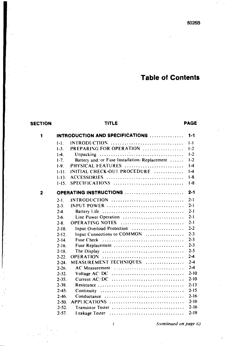
Table of Contents
SECTION TITLE PAGE
1 INTRODUCTION AND SPECIFICATIONS 1-1
1-1. INTRODUCTION 1-1
1.1.
PREPARING FOR OPERATION 1-2
1-4. Unpacking 1-2
1-7. Battery and'or Fuse Installation/Replacement 1-2
1-9. PHYSICAL FEATURES 1-4
1-11.
INITIAL CHECK-OUI PROCEDURE 1-4
1-13. ACCESSORIES 1-8
1-15. SPECIFICATIONS 1-8
2 OPERATING INSTRUCTIONS 2-1
2-1.
jNTRODUCnON 2-1
2-.V INPUT POWER 2-1
2-1.
Battery Life 2-1
2-6.
Line Power Operation 2-1
2-8. OPERATING NOTES 2-1
2-10. Input Overload Protection 2-2
2-12. Input Connections to COMMON 2-3
2-14. Fuse Check ;... 2-3
2-16. Fuse Replacement 2-3
2-18.
The Display 2-3
2-22. OPERATION 2-4
2-24. MEASUREMENT TECHNIQUES 2-4
2-26. AC Measurement 2-4
2-32.
Voltage AC DC 2-10
2-35.
CurremAC.'DC 2-10
2-39. Resistance 2-13
2-43. Continuity 2-15
2-46. Conductance 2-16
2-50. APPLICATIONS 2-16
2-52. Transistor Tester 2-16
2-57.
leakage Tester 2-19
;• (continued on page ii)
Page 5
8026B
TABLE OF CONTENTS, continued
SECTION TITLE PAGE
3 THEORY OF OPERATION 3-1
3-1.
INTRODUCTION 3-1 .
3-3. OVERAI.l. FUNCTIONAL DESCRIPI ION 3-1
3-8. BLOCK DIAGRAM ANALYSIS 3-1
3-9. A/ V Converter 3-1
3-18. Input Signal Conditioners 3-6
4 MAINTENANCE 4-1
4-1.
INTRODUCTION 4-1
4-3,
SERVICE INFORMATION 4-1
4-7.
GENERAL INFORMAIION 4-2
4-8.
Access Information 4-2
4-17.
Cleaning 4-5
4-19.
Battery/Backup Fuse Replacement 4-5
4-21.
PERFORMANCE TES I 4-6
4-23.
Initial Procedure 4-6
4-25.
Display lest 4-6
4-27.
Resistance/Conductance lest 4-7
4-29.
Continuity Test 4-7
4-31.
DC Voltage Test 4-8
4-33.
AC Voltage Test 4-8
4-35.
DC Current 1 est 4-9
4-37.
CALIBRATION 4-10
4-40.
IROUBLESHOOTING 4-11
5 LIST OF REPLACEABLE PARTS 5-1
5-1.
INTRODUCTION 5-1
5^. HOW TO OBTAIN PARTS 5-1
6 ACCESSORY INFORMATION 6-1
6-1.
INTRODUCTION 6-1
6-3. DELUXE CARRYING CASE (C-90) 6-1
6-5. TEMPERATURE PROBE (80T-I50C and 80T-I50K) . 6-1
6-6. Introduction 6-1
6-8. Specifications , 6-1
6-9. CURRENT TRANSFORMER (801-600) 6-4
6-10. Introduction 6-4
6-12. Specifications 6-4
6-13. HIGH VOLTAGE PROBE (80K-6) 6^
6-14. Introduction 6-4
6-16. Specifications 6-4
6-17. HIGH VOLTAGE PROBE (80K-40) 6-4
6-18. Introduction 6-4
6-20. Specifications 6-4
6-21.
HIGH FREQUENCY PROBE (83RF) 6-5
// (continued on page iii)
Page 6
8026B
TABLE OF CONTENTS, continued
SECTION TITLE PAGE
6-22. Introduction 6-5
6-24. Specifications 6-5
6-25. HIGH FREQUENCY PROBE (85RF) 6-5
6-26. Introduction 6-5
6-28. Specifications 6-5
6-29. BATTERY ELIMINATOR (A81-115) 6-6
6-31.
CURRENT SHUNT (80J-10) 6-6
6-32. Introduction 6-6
6-34. Specifications 6-7
6-35. AC/TX'CURRENT PROBE (Y8100) 6-7
6-36. Introduction 6-7
6-39. .Specifications 6-7
6-40. AC CURRENT TRANSFORMER (Y810I) 6-8
6-41 Introduction 6-8
6-43. Specifications 6-8
6^. SAFETY DESIGNED TEST LEAD SF I (Y8132) .... 6-8
6^6. DEI.U.XF TEST LEAD SET (Y81-34) 6-8
6-48. SLIM FLEX TEST LEAD SEI (Y8140) 6-8
7 SCHEMATIC DIAGRAIMS 7-1
APPENDIX A A-1
Page 7
8026B
List of Tables
TABLE TITLE PAGE
1-1
1-2
1-3
2-1
2-2
4-1
4-2
4-3
4-4
4-5
4-6
5-1
5-2.
5-3
5^.
6-1
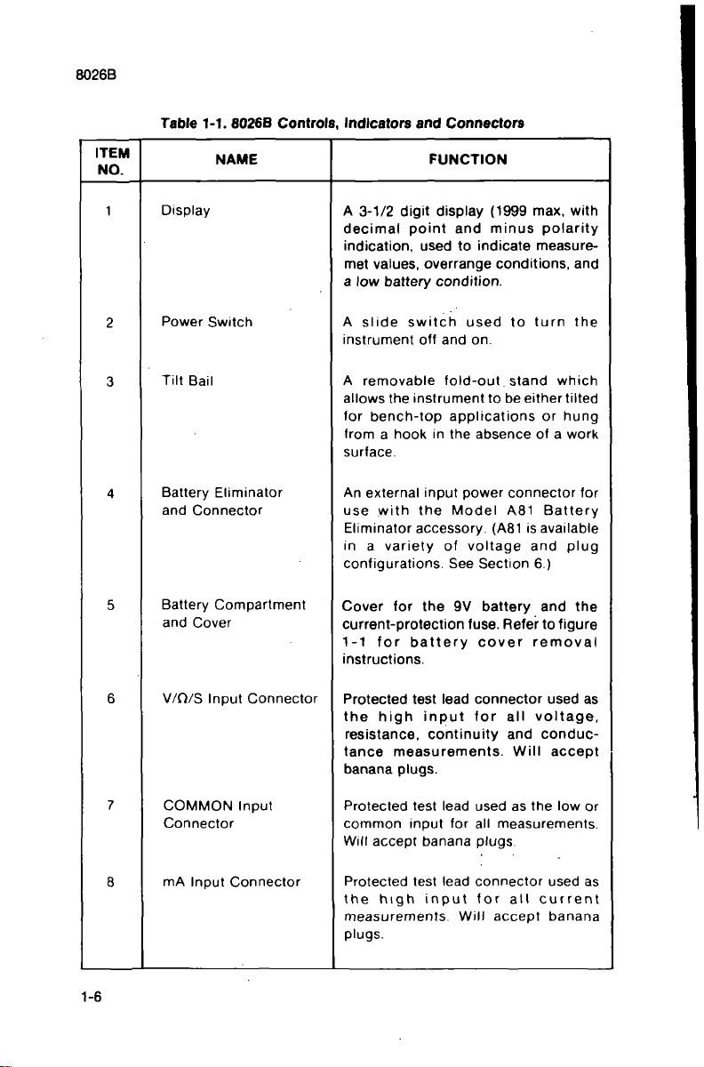
8026B Controls. Indicators and Connectors 1-6
8026B Accessones 1-9
8026B Specifications 1-9
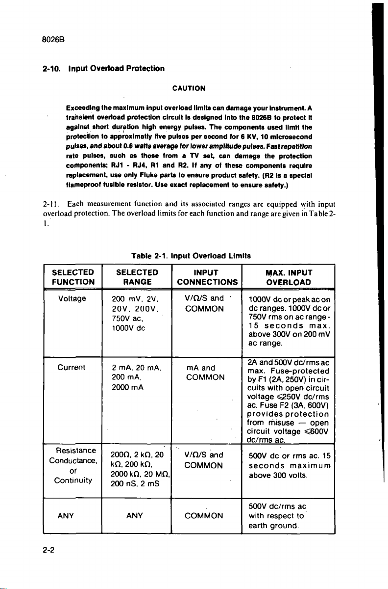
Input Overload Limits 2-2
Voltage/Current Capability of Resistance Ranges 2-15
List of Recommended Test Equipment 4-2
Resistance/ Conductance Checks 4-7.
DC Voltage Checks 4-8.
AC Voltage Test 4-9.
DC Current (mA) Checks 4-10
Troubleshooting Guide 4-12
8026B Final Assembly 5-3.
AI Main PCB Assembly 5-6.
A2 Annunciator PCB Assembly 5-10
Federal Supply Codes for Manufacturers 5-12
A8I Model Numbers and Input Power 6-6
Page 8
8026B
List of illustrations
FIGURE TITLE PAGE
I-I. Removing the Battery Cover 1-3
I-2. Battery Removal 1-4
1-3. Controls, Indicators and Connectors 1-5
2-1.
Volts Operation 2-5
2-2.
Current Operation 2-6
2-3.
Resistance Operation 2-7
2-4.
Conductance Operation 2-8
2-5. Continuity Operation 2-9
2-6.
Waveform Conversion 2-11
2-7.
Voltage Measurement Error Calculations 2-12
2-8. Current Measurement Error Calculations 2-14
2-9. Conductance-to-Resistance Conversion 2-17
2-10. Transistor Beta Test Fixture 2-18
3-1.
Model 8026B Simplified Block Diagram 3-3
3-2. Dual Slope A/ D Converter 3-4
3-3. Input Signal Conditioners 3-8
4-1.
Calibration Adjustment Locations 4-3
4-2.
LCD Display Assembly 4-4
5-1.
8026B Final Assembly 5-5
5-2. Al Main PCB Assembly 5-9
5-3. A2 Annunciator PCB Assembly 5-11
6-1.
8026B Accessories 6-2
v/v;
Page 9
8026B
Section 1
Introduction and Specifications
1-1.
INTRODUCTION
1-2. Your John Fluke Model 8026B is a pocket-size digital multimeter that is ideally
suited for application in the field, lab, shop or home. Some of the features of your
instrument are:
• All VOM functions plus conductance and continuity (8 in all) are included as
standard.
DC Voltage - 100 /iV to lOOOV
AC Vohage - IOO ^lV to 750V
DC Current - I /lA to 2000 mA
AC Current - 1 jiA to 2000 mA
Resistance - 0. in - 20 Mn
Diode Test
Conductance - O.I ns to 200 ns and .001 ms to 2 ms (S = Siemens = 1/n).
Continuity - Provides an immediate audible indication when continuity is
detected.
• True rms ac measurement for signals up to 10 kHz.
• CONDUCFANCE - Allows fast, accurate, noise-free resistance measurements up
to 10,000 Mn.
• An easy-to-read high contrast 3 1/2 digit liquid crystal display.
• Each range has: .
Full auto-polarity operafion
Overrange indication
Effective protection from overloads
• Dual slope integration measurement technique to ensure noise-free measurements.
• Easy calibration - few adjustments.
1-1
Page 10

8026B
Lightweight - 369 grams (13 ounces).
Up to 200 hours of continuous operation can be expected from a single,
inexpensive, 9V, alkaline battery (transistor radio/calculator type).
Low battery voltage automatically detected and displayed.
Line operation is possible using a Model A81 Battery Eliminator (see Section 6.
Accessories).
Protected test leads - finger guards on the probes and shrouded contacts on the
connectors discourage accidental contact with circuit voltages.
A full line of accessories that extend the range and scope of your instrument.
1-3. PREPARING FOR OPERATION
1-4. Unpacking
1-5. Your 8026B was packed and shipped in an especially designed protective container.
This manual, the multimeter, one 9V battery, and two test leads (one red and one black)
should be packed in the shipping container. Check your shipment thoroughly. If anything
is wrong with your shipment, contact the place of purchase immediately. If satisfaction is
not obtained, contact the nearest John Fluke Service Center. A list of these service centers
is located at the end of this manual.
1-6. If reshipment is necessary, please use the original shipping container.
container is not available, a new one can be obtained from the John Fluke Mfg. Co., Inc.
Please state the instrument model number when requesting a new shipping container.
1-7. Battery and/or Fuse Installation/Replacement
1-8. Your 8026B is designed to operate on a single, inexpensive, 9V battery ofthe
transistor radio/calculator variety (NEDA 1604). When you receive your 8026B the
battery will not be installed in the DMM. Once the battery is installed, you can expect a
typical operating life of up to 2(X) hours with an alkaline battery or IOO hours with a
carbon-zinc battery. When the battery has exhausted about 80% of its useful life, the BT
indicator will appear in the upper left corner of the display. Your 8026B will operate
properly for at least 20 hours after BT appears. Use the following procedure to install or
replace the battery and to replace the fuse.
WARNING
TO AVOID ELECTRICAL SHOCK HAZARDS REMOVE THE INPUT SIGNAL
AND THE TEST LEADS FROM THE INPUT TERMINALS, AND SET THE
POWER SWITCH TO OFF BEFORE OPENING THE BATTERY
COMPARTMENT.
1.
Set the 8026B power switch to OFF.
2.
Remove the test leads from external circuit connections and from the 8026B
input terminals.
1-2
I f
the original
Page 11
3.
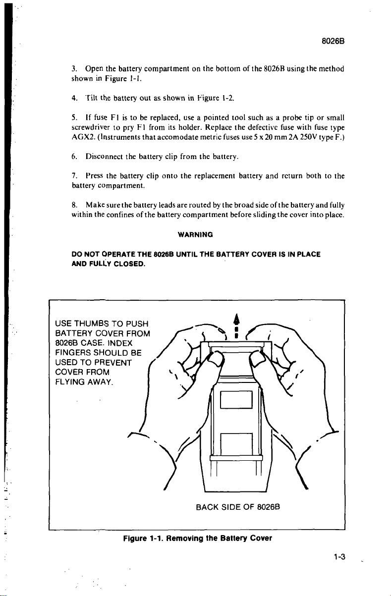
Open the battery compartment on the bottom of the 8026B using the method
shown in Figure 1-1.
4.
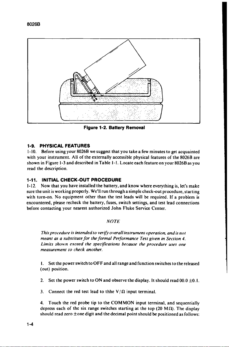
Tilt the battery out as shown in Figure 1-2.
5.
If fuse Fl is to be replaced, use a pointed tool such as a probe tip or small
screwdriver to pry FT from its holder. Replace the defective fuse with fuse type
AGX2.
(Instruments that accomodate metric fuses use 5 x 20 mm 2A 250V type F.)
6. Disconnect the battery clip from the battery.
7.
Press the battery clip onto the replacement battery and return both to the
battery compartment.
8. Make sure the battery leads are routed by the broad side ofthe battery and fully
within the confines ofthe battery compartment before sliding the cover into place.
WARNING
DO NOT OPERATE THE 8026B UNTIL THE BATTERY COVER IS IN PLACE
AND FULLY CLOSED.
USE THUMBS TO PUSH
BATTERY COVER FROM
8026B CASE. INDEX
FINGERS SHOULD BE
USED TO PREVENT
COVER FROM
FLYING AWAY.
8026B
BACK SIDE OF 8026B
Figure 1-1. Removing the Battery Cover
1-3
Page 12
8026B
\
lp^
/^
1
.••r
%^
'^v^i>
" . . .
1^
•^r>--j
:i;s:W
Figure 1-2. Battery Removal
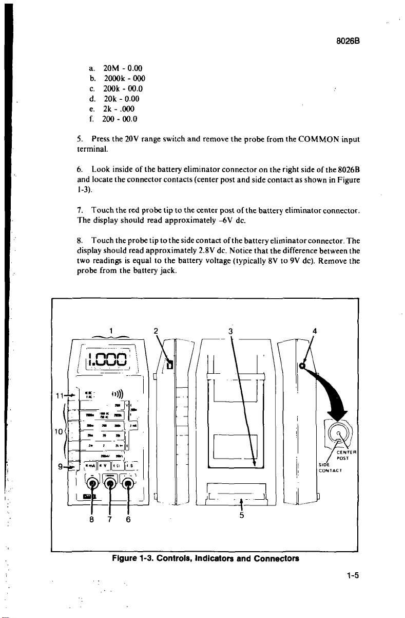
1-9. PHYSICAL FEATURES
1-10. Before using your 8026B we suggest that you take a few minutes to get acquainted
with your instrument. All of the externally accessible physical features of the 8026B are
shown in Figure 1-3 and described in Table 1-1. Locate each feature on your 8026B as you
read the description.
1-11.
INITIAL CHECK-OUT PROCEDURE
1-12. Now that you have installed the battery, and know where everything is, let's make
sure the unit is working properly. We'll run through a simple check-out procedure, starting
with turn-on. No equipment other than the test leads will be required. If a problem is
encountered, please recheck the battery, fuses, switch settings, and test lead connections
before contacting your nearest authorized John Fluke Service Center.
NOTE
This
procedure is intendedto verify overall instrument operation, andisnot
meant as a substitute for the formal Performance Test given in Section 4.
Limits shown e.xceed the specifications because the procedure uses one
measurement to check another.
1.
Set the power switch to OFF and all range and function switches to the released
(out) position.
2.
Set the power switch to ON and observe the display. It should read 00.0 ±0.1.
3.
Connect the red test lead to thhe V/n input terminal.
4.
Touch the red probe tip to the COMMON input terminal, and sequentially
depress each of the six range switches starting at the top (20 Mn). The display
should read zero ±one digit and the decimal point should be positioned as follows:
1-4
Page 13
8026B
a. 20M - 0.00
b.
2000k - 000
c. 200k - 00.0
d. 20k - 0.00
e. 2k - .000
f. 200 - 00.0
5.
Press the 20V range switch and remove the probe from the COMMON input
terminal.
6. Look inside of the battery eliminator connector on the right side of the 8026B
and locate the connector contacts (center post and side contact as shown in Figure
1-3).
7.
Touch the red probe lip to the center post of the battery eliminator connector.
The display should read approximately -6V dc.
8. Touch the probe tip to the side contact ofthe battery eliminator connector. The
display should read approximately 2.8V dc. Notice that the difference between the
two readings is equal to the battery vohage (typically 8V to 9V dc). Remove the
probe from the battery jack.
9-f
, I
non
[_l.tM«OW
'%
i^
8 7 6
Figure 1-3. Controls, Indicators and Connectors
...u
1-5
Page 14
8026B
Table 1-1. 8026B Controls, Indicators and Connectors
ITEM
NO.
1
2
3
4
5
NAME
Display
Power Switch
Tilt Bail
Battery Eliminator
and Connector
Battery Compartment
and Cover
FUNCTION
A 3-1/2 digit display (1999 max, with
decimal point and minus polarity
indication,
met values, overrange conditions, and
a low battery condition.
A slide switch used to turn the
instrument off and on.
A removable fold-out stand which
allows the instrument to be either tilted
tor bench-top applications or hung
from a hook in the absence of a work
surface.
An external input power connector for
use with the Model A81 Battery
Eliminator accessory. (A81 is available
in a variety of voltage and plug
configurations. See Section 6.)
Cover for the 9V battery and the
current-protection fuse. Refer to figure
1-1 for battery cover removal
instructions.
used to indicate measure-
1-6
6
7
8
V/n/S Input Connector
COMMON Input
Connector
mA Input Connector
Protected test lead connector used as
the high Input for all voltage,
resistance, continuity and conductance measurements. Will accept
banana plugs.
Protected test lead used as the low or
common input for all measurements.
Will accept banana plugs
Protected test lead connector used as
the high input for all current
measurements Will accept banana
plugs.
Page 15
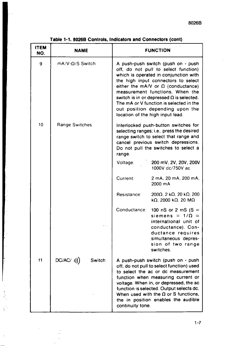
Table 1-1. 8026B Controls, Indicators and Connectors (cont)
ITEM
NO.
NAME
FUNCTION
8026B
10
mA,'V-0/S Switch
Range Switches
A push-push switch (push on - push
off, do not pull to select function)
which is operated in conjunction with
the high input connectors to select
either the mA/V or Q (conductance)
measurement functions. When the
switch is in or depressed O is selected.
The mA or V function is selected in the
out position depending upon the
location of the high input
Interlocked push-button switches for
selecting ranges; i.e., press the desired
range switch to select that range and
cancel previous switch depressions.
Do not pull the switches to select a
range.
Voltage: 200 mV, 2V, 20V, 200V
1000V dc/750V ac
Current: 2 mA, 20 mA. 200 mA.
2000 mA
Resistance: 2000. 2 kO, 20 kO. 200
kO.
Conductance: 100 nS or 2 mS (S =
Siemens = 1/0 =
international unit of
conductance).
ductance requires
simultaneous depression of two range
switches.
lead.
2000 kO. 20 MO
Con-
DC/AC/ I))) Switch
A push-push switch (push on - push
off. do not pull to select function) used
to select the ac or dc measurement
function when measuring current or
voltage. When in, or depressed, the ac
function is selected. Output selects dc.
When used with the O or S functions,
the in position enables the audible
continuity tone.
1-7
Page 16
8026B
9. Depress the lower function button (n) and sequentially depress each of the six
range switches. The display should read I as the most significant digit with no other
numbers shown. This is the standard overrange indication. Notice that the decimal
point changes position with the range switch settings just as it did in step 4 of this
procedure.
10.
Touch the red probe tip to the COMMON input terminal, and sequentially
press each of the range buttons. The display should read zero at each range setting.
Lead resistance may be sufficient to cause one or two tenths
(0.1
or 0.2n) indication
on the 200n range.
11.
Touch the red probe tip to the mA input connector and press the 200n switch.
The display should read 99.0 to lOI.O.
12.
Press the 2 kn switch. The display should read .099 to.
101.
Remove the probe
from the mA input connector.
13.
Simultaneously depress the 2000 kn and the 20 Mn range switches. This
selects the 200 nS range. The display should read 00.0 to OI.O (minimum
conductance, maximum resistance).
14.
Touch the red probe tip to the COMMON input connector. An overrange
indication should be displayed since conductance is the reciprocal of resistance.
15.
Connect the black test lead to the COMMON input connector.
16.
Depress both AC/ DC switch and the 750V ac range switch. Set the mA/ V-n
switch to the voltage (out) position.
WARNING
THE LOCAL LINE VOLTAGE IS MEASURED IN THE FOLLOWING STEP. BE
CAREFUL NOT TO TOUCH THE PROBE TIPS WITH YOUR FINGERS, OR TO
ALLOW THE PROBE TIPS TO CONTACT EACH OTHER.
17.
Measure the local ac line voltage at a convenient output receptacle. The
voltage should be displayed with I volt resolution.
18.
If the 8026B has responded properly to this point, it is operational and ready
for use.
1-13. ACCESSORIES
I-14. Table 1-2 lists the accessories available for use with the Model 8026B. Detailed
information about each accessory is provided in Section 6.
1-15. SPECIFICATIONS
I-16. Table 1-3 lists the 8026B specifications.
1-8
Page 17
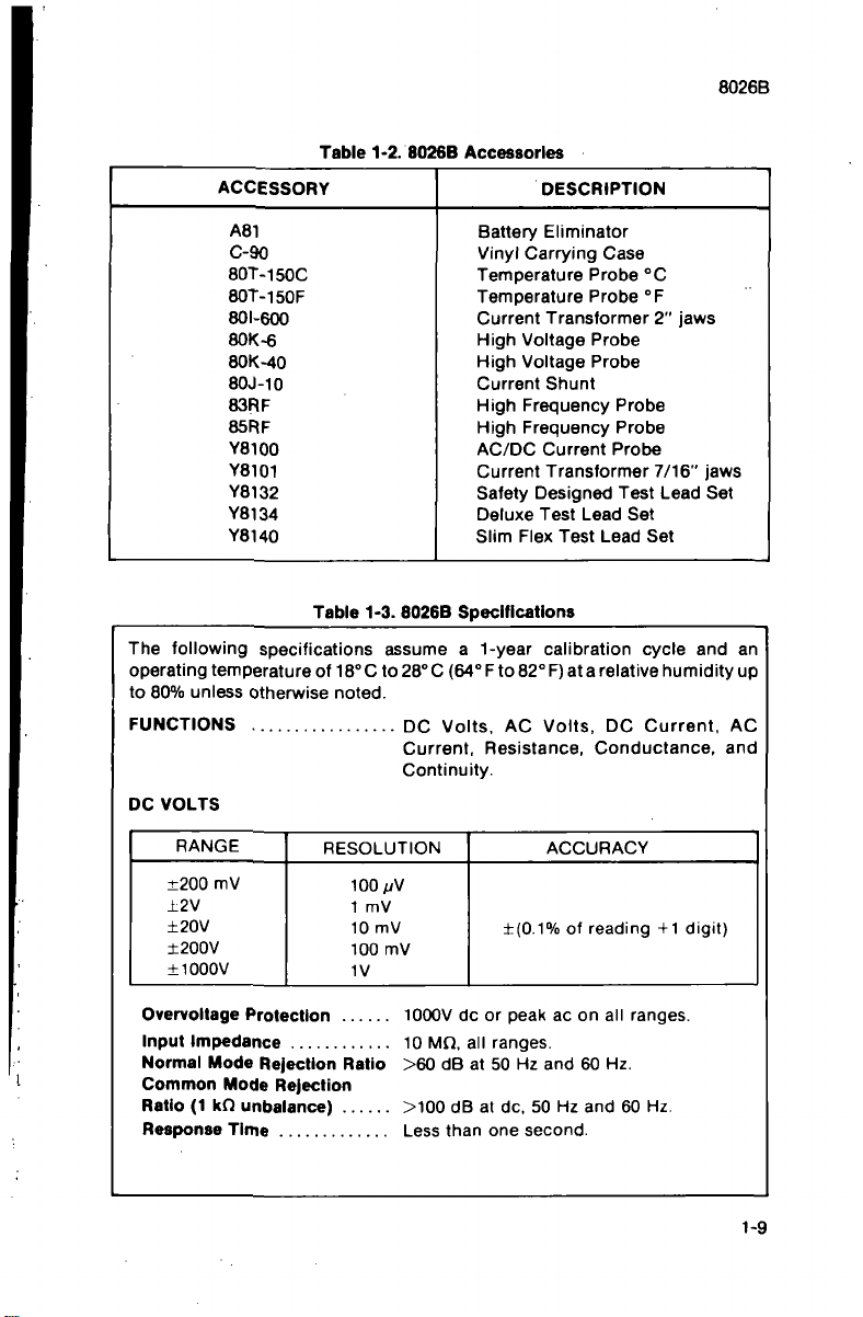
ACCESSORY
Table 1
-2.
8026B Accessories
8026B
DESCRIPTION
A81
C-90
80T-150C
80T-150F
801-600
80K-6
80K-40
80J-10
83RF
85RF
Y8100
Y8101
Y8132
Y8134
Y8140
Table 1-3. 8026B Specifications
The following specifications assume a
operating temperature of
to 80% unless otherwise noted.
FUNCTIONS
DC VOLTS
RANGE
±200 mV
±2V
±20V
±200V
± 1000V
18°
C to 28° C (64° F to 82°
DC Volts, AC Volts, DC Current, AC
Current, Resistance, Conductance, and
Continuity.
RESOLUTION
lOO^V
1 mV
10 mV
100 mV
IV
Battery Eliminator
Vinyl Carrying Case
Temperature Probe °C
Temperature Probe °F
Current Transtormer 2" jaws
High Voltage Probe
High Voltage Probe
Current Shunt
High Frequency Probe
High Frequency Probe
AC/DC Current Probe
Current Transformer 7/16" jaws
Safety Designed Test Lead Set
Deluxe Test Lead Set
Slim Flex Test Lead Set
1-year
calibration cycle and an
F)
at a relative humidity up
ACCURACY
±(0.1%
of reading -1-1 digit)
Overvoltage Protection 1000V dc or peak ac on all ranges.
Input Impedance 10 MO, all ranges.
Normal Mode Rejection Ratio >60 dB at 50 Hz and 60 Hz.
Common Mode Rejection
Ratio (1 kO unbalance) >100 dB at dc, 50 Hz and 60 Hz.
Response Time Less than one second.
1-9
Page 18
8026B
Table 1-3. 8026B Specifications (cont)
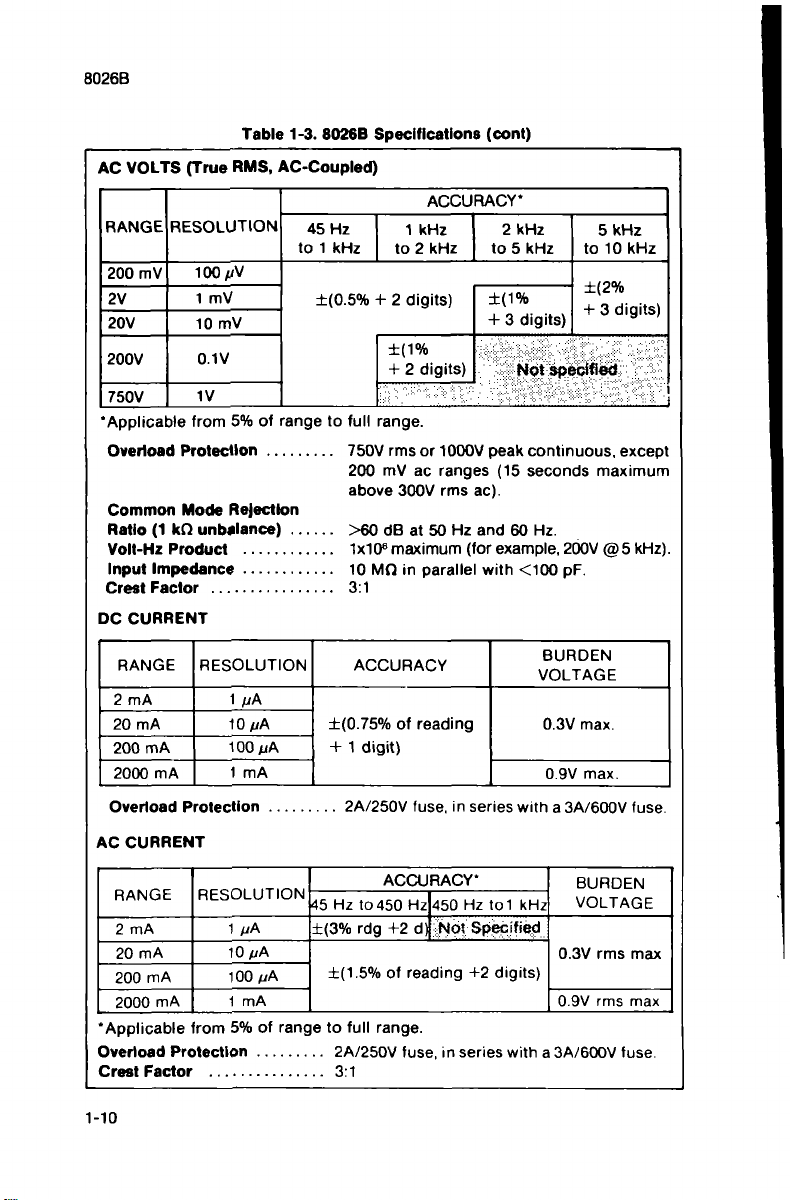
AC VOLTS (True RMS, AC-Coupled)
ACCURACY*
RANGE
200 mV
2V
20V
200V
750V
'Applicable from 5% of range to full range.
Overioad Protection 750V rms or 1000V peak continuous, except
Common Mode Rejection
Ratio (1 kO unbalance) >60 dB at 50 Hz and 60 Hz.
Voll-Hz Product IxW maximum (for example, 200V @ 5 kHz).
Input Impedance 10 MO In parallel with <100 pF.
Crest Factor 3:1
DC CURRENT
RESOLUTION
100
A/V
1 mV
10 mV
0.1V
IV
45 Hz
to 1 kHz
±(0.5%
1 kHz 2 kHz
to 2 kHz to 5 kHz
+ 2 digits)
±(1%
-I-
2 digits)
±(1%
-F 3 digits)
ywitW^^0&^;:-xM
:mmmB
200 mV ac ranges (15 seconds maximum
above 300V rms ac).
5 kHz
to 10 kHz
±(2%
-F 3 digits)
mmm-
RANGE
2 mA
20 mA
200 mA
2000 mA
Overioad Protection
AC CURRENT
RANGE
2 mA
20 mA
200 mA
2000 mA
'Applicable from 5% of range to full range.
Overioad Protection 2A/250V fuse, in series with a 3A/600V fuse.
Crest Factor 3:1
1-10
RESOLUTION
1 pA
10
M
100A(A
1 mA
RESOLUTION
1 pA
10
A/A
100/yA
1 mA
ACCURACY
±(0.75%
+ 1 digit)
45 Hz to 450 Hz
±(3%
±(1.5%
of reading
2A/250V fuse, in series with a 3A/600V fuse.
ACCURACY-
450 Hz tol kHz
rdg +2 d)
jNpt Specjfie^
of reading -t-2 digits)
BURDEN
VOLTAGE
0.3V max.
0.9V max.
BURDEN
VOLTAGE
0.3V rms max
0.9V rms max
Page 19
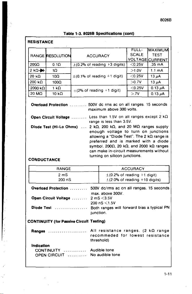
RESISTANCE
RANGE
200n
RESOLUTION
2kn-w-
20 kO
200 kO
2000 kO
20 MO
Table 1-3. 8026B Specifications (cont)
ACCURACY
0.1O
±(0.2%
of reading 1-3 digits)
in
±(0.1%
ion
of reading +^ digit)
loon
1 kn
10 kn
:v(2%
of reading * i digit)
FULL-
SCALE
VOLTAGE
<0.25V
>1.0V
<0.25V
>0.7V
<0.25V
>.7V
8026B
MAXIMUM
TEST
CURRENT
.35 mA
1.1 mA
13/JA
13A(A
0.13/iA
0.13
A/A
Overioad Protection
Open Circuit Voltage
Diode Test (Hi-Lo Ottms)
CONDUCTANCE
RANGE
2 mS
200 nS
Overioad Protection .
Open Circuit Voltage
Diode Test
CONTINUITY (for Passive Circuit Testing)
Ranges All resistance ranges. (2 kn range
Indication
CONTINUITY Audible tone
OPEN CIRCUIT No audible tone
500V dc rms ac on all ranges. 15 seconds
maximum above 3(X) volts.
Less than 1.5V on all ranges except 2 kn
range is less than 3.5V.
2 kn, 200 kn, and 20 Mn ranges supply
enough voltage to turn on junctions
allowing a "Diode Test". The 2 kn range is
preferred and is marked with a diode
symbol.
200n, 20 kn, and 2000 kn ranges
can make in-circuit measurements without
turning on silicon junctions.
ACCURACY
±(0.2%
of reading fl digit)
±(2.0%
of reading +10 digits)
500V dc/rms ac on all ranges. 15 seconds
max. above 300V.
2 mS <3.5V
200 nS <1.5V
Both ranges will forward bias a typical PN
junction.
recommeded for lowest resistance
threshold)
1-11
Page 20
8026B
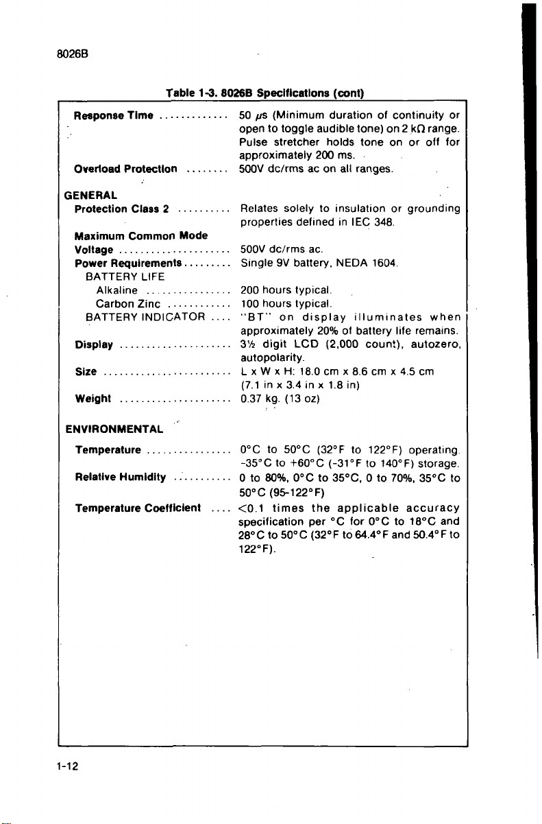
Response Time
Overioad Protection
Table 1-3. 8026B Specifications (cont)
50 ps (Minimum duration of continuity or
open to toggle audible tone) on 2 kO range.
Pulse stretcher holds tone on or off for
approximately 200 ms.
. 500V dc/rms ac on all ranges.
GENERAL
Maximum Common Mode
Voltage
Power Requirements
BATTERY LIFE
Carbon Zinc
BATTERY INDICATOR ..
DisDiav
Size
Weight
ENVIRONMENTAL
Temperature
Relative Humidity
Temperature Coefficient ..
. Relates solely to insulation or grounding
properties defined in lEC 348.
. 500V dc/rms ac.
.. Single 9V battery, NEDA 1604.
.. 200 hours typical.
.. 100 hours typical.
"BT"
on display illuminates when
approximately 20% of battery life remains.
.. 3% digit LCD (2,000 count), autozero,
autopolarity.
.. L X W X H: 18.0 cm x 8.6 cm x 4.5 cm
(7.1 in X 3.4 in x 1.8 in)
.. 0.37 kg. (13 oz)
.. 0°C to 50°C (32° F to 122°F) operating.
-35°C to +60°C (-31 °F to 140°F) storage.
.. 0 to 80%, 0°C to 35°C, 0 to 70%, 35°C to
50° C
(95-122° F)
.. <0.1 times the applicable accuracy
specification per °C for 0°C to 18°C and
28°C to 50°C (32°F to64.4°F and 50.4°F to
122°F).
1-12
Page 21
8026B
Section 2
Operating Instructions
2-1.
INTRODUCTION
2-2.
To fully use the measurement capabilities of your 8026B, a basic understanding of
its measurement techniques and limitations is required. This section of the manual
provides that infonnation. plus a few applications that may prove useful. For example, did
you know your 8026B will provide direct-reading dc current gain (beta) measurements for
both N PN and PN P transistors? Read this section ofthe manual, to find out how it's done.
2-3.
INPUT POWER
2-4.
Battery Life
2-5.
The 8026B is designed to operate on an single, inexpensive 9V battery of the
transistor radio/calulator variety (NEDA 1604). If an alkaline battery is used, a typical
operating life of up to 200 hours can be expected. Carbon-zinc batteries will have a useful
life of up to 100 hours, in either event, the 8026B will display a Bl (in upper, left-hand
corner) when the battery has exhausted approximately 80% of
appears, the battery is capable of properly operating the 8026B for at least another 20
hours.
its
useful life. When Bl first
CAUTION
To ensure multimeter operation within the accuracy specifications, the tiattery
should t>e replaced when the voltage measured at the center of the tiattery
eliminator connector falls below -3.00 volts (with respect to the COMMON
Input). It the battery voltage falls to a point where the"BT" is displayed and the
digital display Is Inactive or no longer responds to an Input signal, the battery
should be replaced Immediately to prevent damage to the LCD.
2-6.
Line Power Operation
2-7.
You can operate your 8026B from line power by using the A81 Battery Eliminator
Accessory. Refer to Section 6 for additional information about the A8I.
2>8.
OPERATING NOTES
2-9.
The following paragraphs will familiarize you with the capabilities and limitations
of your Model 8026B and instruct you in routine operator maintenance.
2-1
Page 22
8026B
2-10. Input Overload Protection
CAUTION
Exceeding the maximum Inpul overload limits can damage your Instrument.
transient overload protection circuit
against short duration high energy pulses.
protection
pulses, and about 0.6 watts average
rate pulses, such
components;
replacement,
flameproof fusible resistor. Use exact replacement
2-11.
Each measurement function and its associated ranges are equipped with input
to
approximatly iWe pulses
as
RJ1 - RJ4, Rl and R2. If any of
use
those Irom
only Fluke parts
Is
designed Into
The
per
lor
lower amplitude
a TV set, can
to
ensure product safety.
components used limit
second
for 6 KV, 10
damage
these components require
to
the
8026B
to
microsecond
pulses.
Fast repetition
the
protection
(R2 Is a
ensure safety.)
protect
the
special
overload protection. The overload limits for each function and range are given
1.
Table 2-1. Input Overload Limits
SELECTED
FUNCTION
Voltage
SELECTED
RANGE
200
mV, 2V,
20V, 200V.
750V
ac,
1000V
dc
INPUT
CONNECTIONS
V/n/S and
'
COMMON
MAX. INPUT
OVERLOAD
10OOV dc
or
peak ac on
dc ranges. 1000V dcor
750V rms on
ac
15 seconds
above 300V on 200 mV
ac range.
Current
2 mA, 20 mA,
200 mA,
2000
mA
mA and
COMMON
2A and 500V dc/rms ac
max. Fuse-protected
byFI (2A, 250V) in circuits with open circuit
voltage
^50V
ac. Fuse
F2
(3A, 600V)
provides protection
from niisuse — open
circuit voltage C600V
dc/rms
ac.
Resistance
Conductance,
or
Continuity
200n, 2 kn,
kn,
200 kn,
2000 kn,
200 nS,
20 Mn,
2 mS
20
V/n/S
and
COMMON
500V
dc or rms ac. 15
seconds maximum
above 300 volts.
A
It
in
Table
range
max.
dc/rms
2-
-
2-2
ANY
ANY
COMMON
500V dc/rms
with respect
to
earth ground.
ac
Page 23
8026B
2-12.
Input Connections to COMMON
WARNING
TO AVOID ELECTRICAL SHOCK AND /OR INSTRUMENT DAMAGE DO
NOT CONNECT THE COMMON INPUT TERMINAL TO ANY SOURCE OF
MORE THAN 500 VOLTS DC OR RMS AC ABOVE EARTH GROUND.
2-13.
The 8026B may be operated with the COM MON input terminal at a potential of up
to 500V dc or 500V rms ac above earth ground, if this limit is exceeded, instrument
damage may occur. This, in turn, may result in a safety hazard for the operator.
2-14. Fuse Check
2-15.
The current (mA) function contains two fuses. Check them as follows:
1.
Complete the set up steps for the RESISTANCE (n) function and select the 2
kn range.
2.
Touch the red test probe to the mA input jack so that the V-n input and m.A
input are connected together.
3.
If the display reads approximately .100 kn, both fuses are good.
4.
If the display reads overrange (a I followed by blank digits), one or both fuses
need replacement. See the following paragraph for replacement instructions.
2-16. Fuse Replacement
2-17.
All ac and dc current ranges are fuse protected. Two series fuses are used:
1.
FI, 2A@ 250V, replaceable at the battery compartment (see section 1 "Battery
or Fuse Installation/Replacement").
2.
F2, 3A@ 600V backup fuse (see section 4, Battery/Backup Fuse
Replacement).
2-18. The Display
2-19. The Front Panel Display on your 8026B is a 3-1/2 digit Liquid Crystal Display.
The 1/2 digit is the extreme left digit location. So, the displayed value can range from000
through 1999. For convenience, in discussion, the 1999 is rounded to 2000. The decimal
point position is determined by selected range and is not affected by the measurement
function selected. Polarity, on the other hand is only used for the dc voltage and current
measurement functions. A minus sign indicates that the input signal is negative with
respect to the COMMON input terminal. Positive inputs are indicated by the absence of
the minus sign.
NOTE
The minus sign (-) may flash momentarily as the 8026 B comes out of an
overrange condition. This will most likely be seen in the ohms mode as the
open circuit lest leads are applied to an in-range resistance value. If the
minus sign remains on for in-range ohms readings, the circuit is live (a
negative voltage
etc.),
and incorrect resistance readings will he observed.
is
pre.sent at the input terminals due to charged capacitors,
2-3
Page 24
8026B
2-20. The Display has two abnormal status indicators, one for low battery power and
one for instrument overrange. A "BT" is displayed when approximately 80% of the
battery's life is exhausted (battery replacement is indicated). And, a "I" followed by three
blanked digits is displayed (decimal point may be present) as an overrange indication. This
does not necessarily mean that the instrument is being exposed to a damaging input
condition. For example, when measuring resistance an open-input will cause an overrange
indication.
NOTE
When the 8026B is powered with the A8I Battery Eliminator the "BV
indicator may come on. However, instrument operation will he normal.
2-21.
1'he liquid crystal display used in the 8026B is a rugged and reliable unit which will
give years of satisfactory service. Display life can be extended by observing the following
practices:
1.
Protect the display from extended exposure to bright sunlight.
2.
Keep the voltmeter out of high temperature, high humidity environments, such
as,
the dash of a car on a hot, sunny day. Otherwise, the display may temporarily
turn black. Recovery occurs at normal operating temperature.
3.
Note that the display operation may be slowed in extremely low temperature
environments. No damage will occur to the LCD, but response time is greatly
increased. Recovery occurs at normal operating temperature.
2-22.
OPERATION
2-23.
The five figures, 2-1 through 2-5, each illustrate one ofthe measurement functions
ofthe Model 8026B. Each figure has two parts. The top part shows your 8026B as it should
look when ready to perform that type of nieasurement. The bottom part ofthe figure lists,
in sequential order, the steps you should perform to make that type of measurement with
your 8026B. To operate your 8026B turn to the operation figure corresponding to the
measurement function desired and perform the steps listed in the figure. Operate the
Model 8026B in accordance with the Input Overload Protection and the Input
Connections to COMMON portions of the Operating Notes presented earlier in this
section.
2-24. MEASUREMENT TECHNIQUES
2-25.
The following paragraphs offer you techniques that improve the measurement
accuracy of your 8026B. While these techniques are in general use throughout the
electronics industry, these paragraphs offer specifiee information for use with your 8026B.
2-26. AC Measurement
2-27.
The 8026B employs a true rms ac converter for ac signal measurements. The true
rms value of an ac signal may be defined as the equivalent dc value that dissipates the same
amount of heat in a resistor as the relative ac signal. Consider the following example: a
light bulb is energized with an ac signal and the brightness is measured. The ac source is
then removed from the light bulb and replaced by a variable dc source. The level of the dc
signal is adjusted so that the brightness of the light bulb is the same as it was for the ac
signal. This dc level is equivalent to the rms value of the ac signal. This cumbersome
method is not practical for handheld multimeters, so an active log-antilog analog
computation is continuously performed on the input signal.
2-4
Page 25
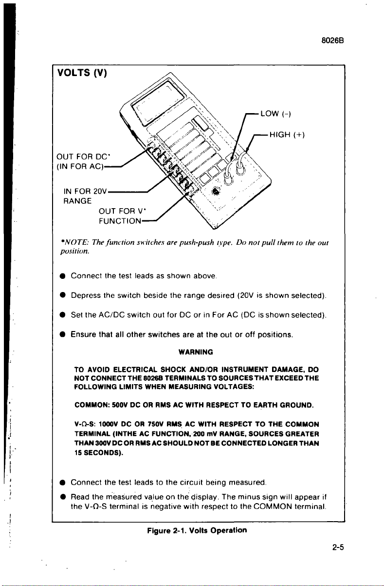
VOLTS (V)
OUT FOR DC
(IN FOR AC)
IN FOR 20V
RANGE
OUT FOR V
FUNCTION
*NOTE: The function switches are push-push type. Do not pull them to the out
position.
• Connect the test leads as shown above.
• Depress the switch beside the range desired (20V is shown selected).
• Set the AC/DC switch out for DC or in For AC (DC is shown selected).
8026B
• Ensure that all other switches are at the out or off positions.
WARNING
TO AVOID ELECTRICAL SHOCK AND/OR INSTRUMENT DAMAGE, DO
NOT CONNECT THE 8026B TERMINALS TO SOURCES THAT EXCEED THE
FOLLOWING LIMITS WHEN MEASURING VOLTAGES:
COMMON:
V-n-S:
TERMINAL (INTHE AC FUNCTION, 200 mV RANGE, SOURCES GREATER
THAN 300V DC OR RMS AC SHOULD NOT BE CONNECTED LONGER THAN
IS SECONDS).
• Connect the test leads to the circuit being measured.
• Read the measured value on the display. The minus sign will appear if
the V-n-S terminal is negative with respect to the COMMON terminal.
500V DC OR RMS AC WITH RESPECT TO EARTH GROUND.
lOOOV DC OR 750V RMS AC WITH RESPECT TO THE COMMON
Figure 2-1. Volts Operation
2-5
Page 26
8026B
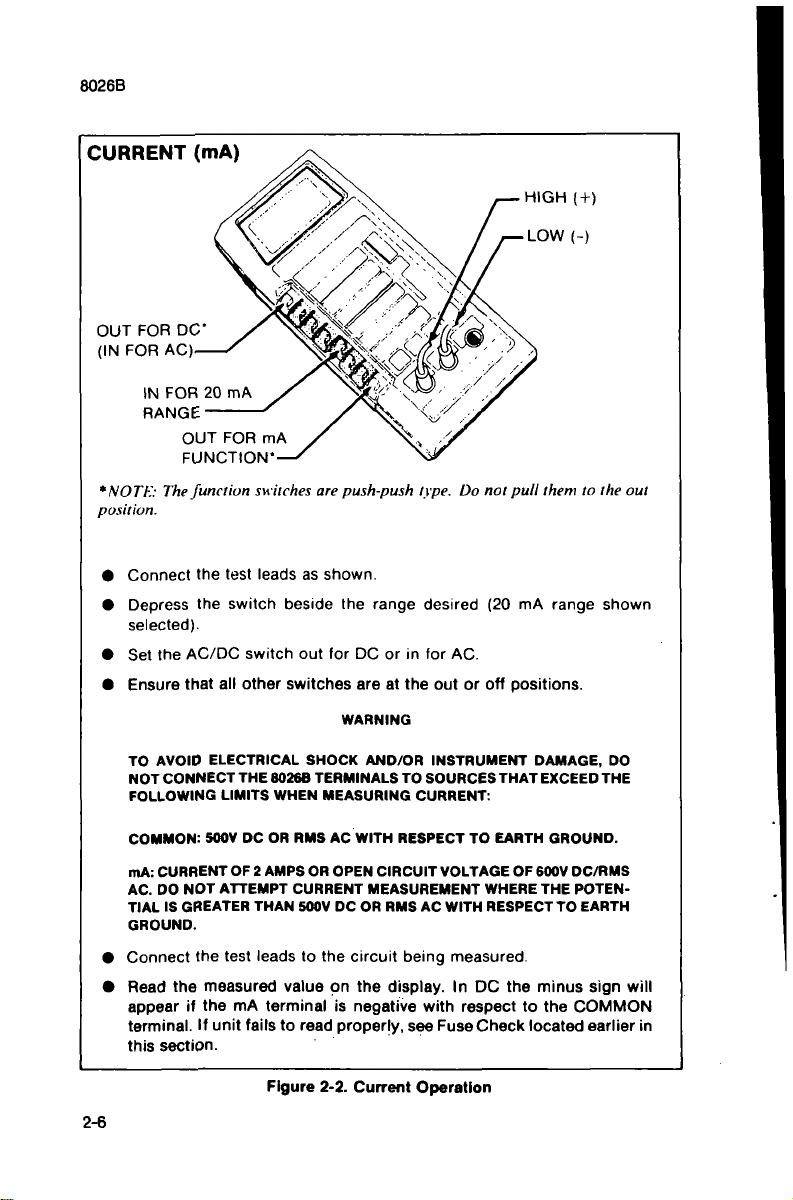
CURRENT (inA)
OUT FOR DC
(IN FOR AC)
IN FOR
RANGE
OUT FO
FUNCTION
*NOTE:
The
position.
• Connect the test leads as shown.
• Depress the switch beside the range desired (20 mA range shown
• Set the AC/DC switch out for DC or in for AC.
• Ensure that all other switches are at the out or off positions.
function switches are push-push type. Do not pull them to the out
selected).
WARNING
TO AVOID ELECTRICAL SHOCK AND/OR INSTRUMENT DAMAGE, DO
NOT
CONNECT
FOLLOWING LIMITS WHEN MEASURING CURRENT:
COMMON:
mA:
CURRENT
AC.
DO NOT ATTEMPT CURRENT MEASUREMENT WHERE THE POTENTIAL IS GREATER THAN
GROUND.
• Connect the test leads to the circuit being measured.
• Read the measured value on the display. In DC the minus sign will
appear if the mA terminal Is negative with respect to the COMMON
terminal.
this section.
2-6
THE 8026B
SOOV
DC OR RMS AC WITH RESPECT TO EARTH GROUND.
OF 2
If unit falls to read properly, see Fuse Check located earlier in
TERMINALS
AMPS
OR OPEN
SOOV
DC OR
Figure 2-2. Current Operation
TO SOURCES THAT EXCEED
CIRCUIT VOLTAGE
RMS
AC WITH RESPECT
OF 6(X)V
TO
DC/RMS
EARTH
THE
Page 27
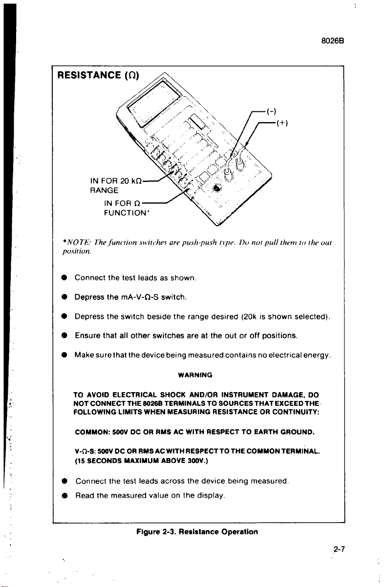
RESISTANCE (Q) /<\
IN FOR 20 kn
RANGE
IN FOR n
FUNCTION
*NOTE: The function switches are push-push type. Do not pull them to the out
position.
• Connect the test leads as shown.
• Depress the mA-V-O-S switch.
• Depress the switch beside the range desired (20k is shown selected).
8026B
• Ensure that all other switches are at the out or off positions.
• Make sure that the device being measured contains no electrical energy.
WARNING
TO AVOID ELECTRICAL SHOCK AND/OR INSTRUMENT DAMAGE, DO
NOT CONNECT THE 8026B TERMINALS TO SOURCES THAT EXCEED THE
FOLLOWING LIMITS WHEN MEASURING RESISTANCE OR CONTINUITY:
COMMON:
V-n-S:
(15 SECONDS MAXIMUM ABOVE SOOV.)
• Connect the test leads across the device being measured.
• Read the measured value on the display.
SOOV DC OR RMS AC WITH RESPECT TO EARTH GROUND.
SOOV DC OR RMS AC WITH RESPECT TO THE COMMON TERMINAL.
Figure 2-3. Resistance Operation
2-7
Page 28
8026B
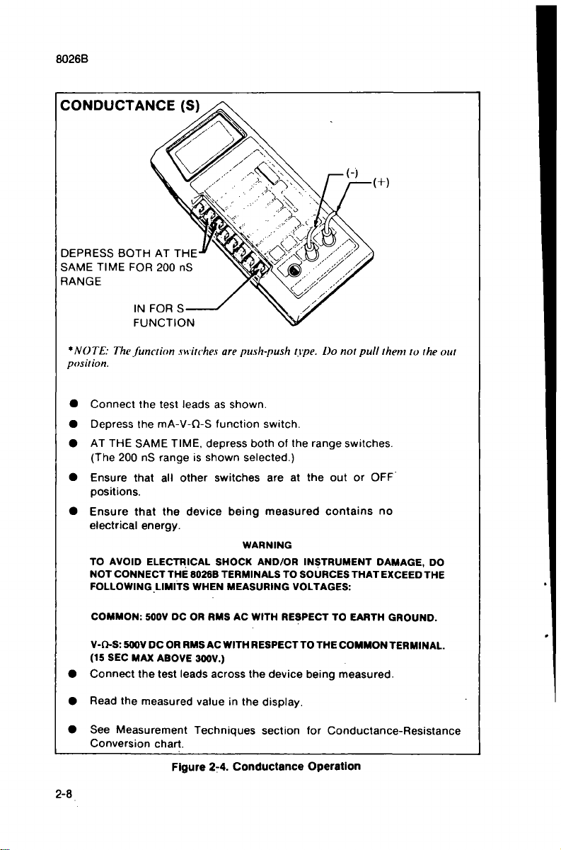
CONDUCTANCE (S)
DEPRESS BOTH AT THE
SAME TIME FOR 200 nS
RANGE
IN FOR S —
FUNCTION
*NOTE: The function switches are push-push type. Do not pull them to the out
position.
Connect the test leads as shown.
Depress the mA-V-O-S function switch.
AT THE SAME TIME, depress both of the range switches.
(The 200 nS range is shown selected.)
Ensure that all other switches are at the out or OFF
positions.
Ensure that the device being measured contains no
electrical energy.
WARNING
TO AVOID ELECTRICAL SHOCK AND/OR INSTRUMENT DAMAGE, DO
NOT CONNECT
FOLLOWING LIMITS WHEN MEASURING VOLTAGES:
THE 8026B
TERMINALS
TO SOURCES
THAT
EXCEED
THE
COMMON:
V-O-S:
(15 SEC MAX ABOVE SOOV.)
Connect the test leads across the device being measured.
Read the measured value in the display.
See Measurement Techniques section for Conductance-Resistance
Conversion chart.
2-8
SOOV
SOOV
DC OR RMS AC WITH RESPECT TO EARTH GROUND.
DC
OR RMS AC WITH RESPECT TO THE COMMON
Figure 2-4. Conductance Operation
TERMINAL.
Page 29

CONTINUITY
IN FOR
AUDIBLE TONE
IN FOR 2 kn FUNCTION
IN FOR n FUNCTION
*NOTE:
The
position.
• Connect the test leads as shown.
• Depress the mA-V-n-S function switch.
• Depress the 2 kn range switch.
function switches are push-push type. Do not pull them to the out
8026B
• Depress the AC/DC function switch.
• Ensure that all other switches are at the out position.
• Ensure that the device being measured contains no
electrical energy.
WARNING
TO AVOID ELECTRICAL SHOCK AND/OR INSTRUMENT DAMAGE, DO
NOT
CONNECT
FOLLOWING LIMITS WHEN MEASURING CONDUCTANCE:
COMMON:
V-n-S:
SOOV DC OR RMS AC WITH RESPECT TO THE COMMON
(15 SEC MAX ABOVE SOOV.)
• Connect the leads to the circuit being measured.
• Continuity between the test leads will cause the audible tone to sound.
THE 6026B
SOOV
DC OR RMS AC WITH RESPECT TO EARTH GROUND.
Figure 2-5. Continuity Operation
TERMINALS
TO SOURCES
THAT
EXCEED THE
TERMINAL.
2-9
Page 30
8026B
2-28.
It should be noted that accurate measurements can only be guaranteed for ac input
signals that have some reasonable limits with regard to the frequency and shape ofthe
waveform. To help define what these reasonable limits are. a parameter known as "crest
factor" has been developed. Crest factor is defined as the peak signal value divided by the
rms value of the signal (with any dc component removed). Forexample, the crest factor of
a
10%
duty-cycle rectangular pulse train is 3.16, and the crest factor of a sine wave is 1.41.
2-29. It should also be noted that signals with high crest factors usually have wide
bandwidth requirements which may be near the specified frequency limits for the selected
range. Both crest factor and frequency response should be carefully considered when
evaluating reading accuracies. Refer to Section 1 for the 8026B specifications for ac
measurements.
2-30. Most analog and digital multimeters use average-responding ac converters. The
gain in an average-responding ac converter is adjusted so that the multimeter measures
sinusoidal signals correctly. However, if a signal is not perfectly sinusoidal, the multimeter
with the average-responding ac converter will not measure the signal correctly. Figure 2-6
shows how the 8026B readings compare with average-responding multimeter readings for
seven common waveforms.
2-31.
You can also use the values in Figure 2-6 to calculate other waveform parameters
from readings displayed on the 8026B. For example, if a rectified full wave sine wave is
being measured and the 8026B displays the value 0.435 (V ac). then the pk-pk vohage
would be
1.414V
(the same as the 0-pk voltage). The dc component would be 0.900V (this
could be verified by switching to the dc volts function). For another example, suppose the
8026B measures a rectified half wave sine wave and displays the value 1.000
pk or 0-pk voltage would be
1 OOOV
x (2.000
-=-
0.771) = 2.594V. The dc component would
(V
ac). The pk-
be l.tXWV X (0.636 -r 0.771) = 0.825V. For this same signal, an average-responding
multimeter would measure I.OOOV x (0.764 -=- 0.771) = 0.991V, an error of 0.9%.
2-32.
Voltage AC/DC
2-33.
The 8026B is equipped with five ac and five dc voltage ranges; 200 mV, 2V, 20V,
2(X)V. 750V ac/
ICMXIV
dc. All ranges present an input resistance of 10 Mil shunted by less
than IOO pF. When making measurements, be careful not to exceed the overload limits
given earlier in lable 2-1.
2-34. Measurement errors, due to circuit loading, can result when making either ac or dc
voltage measurements on circuits with high source resistance. However, in most cases the
error is negligible «0.1%) as long as the source resistance of the measurement circuit is 10
kn or less. If circuit loading does present a problem, the percentage of error can be
calculated using the appropriate formula in Figure 2-7.
2-35. Current AC/DC
WARNING
WHEN MEASURING CURRENT, DO NOT EXCEED THE
MAXIMUM COMMON MODE VOLTAGE SPECIFICATION FOR THE
INSTRUMENT. THE OPERATOR IS PROTECTED FROM POSSIBLE INJURY
AND THE INSTRUMENT IS PROTECTED FROM POSSIBLE DAMAGE BY A
250V FUSE IN SERIES WITH A SOOV FUSE.
2-10
SOOV
DCOR RMS AC
Page 31

8026B
AC-COUPLED
INPUT
WAVEFORM
SINE
PK
1
RECTIFIED SINE
(FULLWAVEI
RECTIFIED SINE
(HALF WAVEl
^/\/\p^K
SQUARE
O' . PK PK
RECTIFIED
SQUARE
PK PK-i
RECTANGULAR
PULSt
"^r^ rn +
-M Y U- t
D - X, Y
K Vl3 - D'
TRIANGLE
SAWTOOTH
PK
0^^ PK^K
PEAK VOLTAGES
PK-PK
2
8?8
1
414
2.000
2000
1
414
2.000
3464
0-PK
1.414
1
414
2 000
1.000
1.414
2.000
1.732
DISPLAY HtADINGS
AC COMPONENT ONLY
RMS CAL
AVE SENSING
1
0.421
0 764
1111
0.786
2 22IK
0.960
RMS SENSING
000
(80268)
1.000
0 435
0 771
1.000
0.707
2K
1.000
DC
COMPONENT
ONLY
0 000
0 900
0 636
0.000
0.707
2D
0000
DC AND AC
TOTAL RMS
TRUE RMS =
\''ac' • dc
=
1.000
1
000
1.000
1.000
1.000
2\^
1
000
NOTE:
High Frequency waveforms with fairly abrupt transitions (such as a
5 kHz pulse with a 10% duty cycle) have spectral components that are
beyond the specified frequency limits for the selected range. Be sure to take
this into account when evaluating measurements.
Figure 2-6. Waveform Conversion
2-11
Page 32

8026B
1.
DC VOLTAGE MEASUREMENTS
Loading Error in % = 100 x Rs^ (Rs + 10')
Where: Rs = Source resistance in ohms of circuit
2.
AC VOLTAGE MEASUREMENTS
First, determine input impedance, as follows:
Zin
Where: Zin — effective input impedance
Rin = 10' ohms
Cin = 100 X 10-" Farads
F = frequency in Hz
Then,
determine source loading error as follows:
being measured.
lO:
v/l + (2n F 'Rin'O'
Loading Error in %
Where: Zs = source impedance
Zin = input impedance (calculated)
"Vector algebra required
Figure 2-7. Voltage Measurement Error Calculations
2-36. Four ac and four dc current ranges are included on the 8026B; 2 mA, 20 mA, 200
mA, and 2000 mA: Each range is diode protected to 2 amps and fuse protected above 2
amps.
If either fuse blows, refer to fuse replacement information given earlier in this
section.
2-37.
In high elearical noise environments (near ignition switches, fiourescent lights,
relay switches, etc.) unstable or erroneous readings (exceeding specifications) may occur.
The effect is most obvious when measuring low level current on the 2 mA range. If an
2-12
100 xZs
Zs + Zin
Page 33

8026B
erratic or erroneous reading is suspected, temporarily jumper the V/n connector to the
mA connector. This is recommended for the 2 mA and 20 mA ranges only.
CAUTION
To avoid pos8lt>le Instrument damage and/or erroneous measurements
remove the temporary V/O-to-mA jumper l>efore attempting voltage or
resistance measurements.
2-38.
Full-scale burden voltage (voltage drop across the fuse and current shunt) for all
ranges except 2000 mA is less than 300 mV. The 2000 mA range has a full-scale burden
voltage of less than 900 mV. These voltage drops can affect the accuracy of a current
measurement, if the current source is unregulated and the shunt plus fuse resistance
represents a significant portion (l/IOOO or more) of the source resistance. If burden
voltage does present a problem, the percentage of error can be calculated using the
formula in Figure 2-8. This error can be minimized by using the highest current range that
gives the necessary resolution. For example, if 20 mA is measured on the 2000 mA range
the burden voltage is approximately 5 mV.
2-39. Resistance
2-40. Six direct reading resistance scales are provided on the 8026B: 20 Mn, 2000 kn,
200 kn, 20 kn, 2 kn and 200n. All scales employ a two-wire measurement technique. As a
result, test lead resistance may influence measurement accuracy on the 200n range. To
determine the error, short the test leads together and read the lead resistance. Correct the
measurement by subtracting the lead resistance from the measurement reading. The error
is generally on the order of 0.2 to 0.3 ohms for a standard pair of test leads.
2-41.
In-circuit resistance measurements can be made using the 200n, 20 kfl and 2000
kn ranges. The full scale measurement voltage produced on these ranges is not sufficient
to forward bias silicon diode/ emitter-base junctions, and thus, enables resistance values to
be measured without removing diodes and transistors from the circuit. Conversely, the 2
kn, 200 kn, and 20 Mn ranges produce a measurement voltage sufficient to forward bias a
P-N junction. These ranges enable both diode- and transistor-junction checks to be made
conveniently. Full scale voltage and short circuit current for each resistance range is given
in Table 2-2. All values shown are referenced to the COMMON input terminal; i.e., the
V/n/S terminal is positive.
NOTE
A
ny change (greater than one or two digits) in apparent resistance when test
leads are reversed may indicate either the presence of a diode junction or a
voltage in the circuit.
CAUTION
Tum test circuit power off and discharge all capacitors before attempting Inclrcult resistance measurements.
2-13
Page 34

8026B
Es-r-
Es = Source voltage
RL
= Load resistance + Source resistance
1^
= Measured current (display reading in mA)
EB
= Burden voltage (calculated), i.e.. Display reading
expressed asa%offull-scale(100x
FULL-SCALE
^
times full-scale burden voltage for selected range. See
Table.
RANGE
2 mA to 200 mA
2000 mA
MAXIMUM
BURDEN VOLTAGE
0.3V
0.9V
Maximum current error due to Burden Voltage:
Error in %
Error in mA
= 100
EBX'M
Es -EB
X
=B
ES-EB
Example: Es = 14V, RL = 90, I^/I = 1497 mA,
Eg = 100
1497
X 0.9 (from Table)
2000
749% X 0.9 ^ 0.674V
Error in % = 100
.674
14-674 ' 13.326
100
.674
5.06%
Increase displayed current by 5.06% to obtain true current.
2-14
Error in mA
_ .674 X 1497 1009
14 - .674 13.326
76 mA
Increase displayed current by 76 mA to obtain true current.
Figure 2-8. Current Measurement Error Calculations
Page 35

Table 2-2. Voltage/Current Capability of Resistance Ranges
RANGE
FULL-SCALE
VOLTAGE (TYPICAL)
SHORT CIRCUIT
CURRENT (TYPICAL)
8026B
20 Mn
2000 kn
200 kn
20 kn
2kn-w2oon
2-42. Three of the 8026B resistance ranges have a high enough open-circuit voltage to
turn on a silicon junction. These ranges (2 kn. 200 kn, and 20 Mn) can be used to check
silicon diodes and transistors. The 2 kn range is preferred for this function and is marked
with a diode symbol. The open-circuit voltage of the three alternate ranges (200n, 2 kn,
and 2 Mn) is not high enough to turn on a silicon junction. Use these three ranges to make
in-circuit resistance measurements. For all resistance ranges, the V/n/S input terminal is
positive with respect to the COMMON input terminal.
2-43. Continuity
2-44. Audibly confirmed continuity measurements may be made using any of the
resistance or conductance ranges. The 2 kn range is recommended for this mode since it
provides the lowest resistance threshold, approximately 110 ohms. On this range a
measured resistance lower than 110 ohms initiates the audible tone. To determine the
exact threshold, use a variable resistor and observe the display reading at which the tone
switches on and/ or off. Note that in this mode resistance or conductance readings are also
displayed. However, high resistance ranges and the 200 nS range may exhibit noisy or
drifting readings due to ambient signal noise.
2-45.
Intermittent open or short circuits with a duration of at least 50
the 2 kn range. A continuously intermittent connection is heard as a series of beeps. A
series of beeps (due to environmental noise) is also encountered when a measurement is
near the threshold of the selected range. The approximate thresholds for the continuity
ranges are as follows:
+800 mV
+200 mV
+800 mV
+200 mV
+ 1.1V
+55 mV
+0.12
A/A
+0.12
AiA
+ 12AiA
+^2^^
+ 1.0 mA
+0.3 mA
jus
are detectable in
RANGE
200 nS
2mS
20 MO
2000 kn
200 kn
20 kn
2kn
20on
THRESHOLD
900 kilohms
110 ohms
900 kilohms
900 kilohms
9 kilohms
9 kilohms
110 ohms
360 ohms
2-15
Page 36

8026B
2-46. Conductance
2-47.
The conductance ranges, (2(X) nS and 2 mSjare included on the 8026B for making
both conductance and resistance measurements. When either range is selected the display
reads the measurement resuhs in terms of conductance
required, refer to the conductance-to-resistance conversion information given in F'igure
2-9.
2-48.
The 200 nS range is intended for use in making fast, accurate, high-resistance
measurements from 5 Mn to 10,000 Mn. Ordinarily, resistance measurements within this
range are plagued by noise pick-up and require careful shielding. However, by measuring
the resistance in terms of conductance, standard test leads are adequate for the 8026B to
make noise-free measurements up to 10,000 Mn. High value resistors, and low leakage
components (i.e., diodes, etc.) are natural candidates for the 200 nS conductance range.
Refer to applications later in this section for additional information.
2-49. The 2 rriS range, in terms of resistance, starts at 500n and goes up to 1 Mn. It is
intended for use in making either resistance measurements or direct-reading dc current
gain (beta) measurements on transistors. Beta measurements require the use of a special
test fixture, and are discussed later in this section under applications.
2-50. APPLICATIONS
2-51.
The applications described in the following paragraphs are suggested as useful
extensions of the 8026B measurement capabilities. However, they are not intended as the
equivalent of a manufacturer's recommended test methods. Rather, they are intended to
provide repeatable and meaningful indications which will allow operator to make sound
judgments concerning the condition of the device being tested; i.e., good, marginal, or
defective.
(1
/ n). if resistance readings are
2-52. Transistor Tester
NOTE
The transistor tester described in the following paragraphs provides
approximate test information. Beta is measured using a VCE of about 2
and an IC of about 200 fiA. The test method is very useful for making
comparative and matching measurements.
2-53.
Select the 2 mS range, plug the fixture shown in Figure 2-10 into the V/n/S and
COMMON input terminals, and you have tranformed your 8026B into a transistor tester.
Now, plug a transistor into the test socket and the 8026B will determine the following:
1.
Transistor type (NPN or PNP).
2.
Collector-to-emitter leakage (ICEs).
3.
Beta from 1 to KKX) without changing range.
2-16
V
Page 37

*mS-to-kO
2
mS
(I'mS
inS
k(^
c
o
ro
ID
o
o
O
o
3
<
•
3
•
20-]
1
0;
05-
02-
0.1;
005-
0
03-
0
01;
0
005-
0
002-
0
001
-
Conversi
o
*
S=
Siemens
of conductance
mho.
to
I
•nS-to-kQ
Range
200
nS
(1000/nS
nS
un
200-
100;
50-
20-
10 =
5-
2-
1;
0 5-
02-
0 1-
Range
-
= kO)
-5
:i
-2
-5
= 10
-20
-50
= 100
-200
-
-500
=1000
on Scales
li\=International unit
= 1
formerly known as the
=Mn)
-i
= 10
r20
L
-50
= 100
-200
-500
= 1000
-2000
-
-sooo
= 10000
NO.
1
2
3
4
5
6
7
a
9
Find the approximate resistance value using one of
the scales
the most significant digit
the vertical NO. column, and
horizontal NO. row. The number
coordinates represents
value.
at
left. Then,
on
of
the
For example, a reading
the table below, locate
the display reading
the
next digit
at
the intersecting
unknown resistance
of
52.0 nS
is
equal
19.2 Mn. Decimal point location is determined from
the scale approximation.
Interpolation Table (I/no.)
.0
1
.500
.333
.250
.200
.167
.143
.125
111
.1
.909
.476
.323
.244
196
.164
.141
.123
.110
.2
.833
.455
.313
.238
.192
.161
.139
122
.109
.3
.769
.435
.303
233
.187
137
.108
159
121
.4
.714
.417
294
.227
.185
156
135
.119
.106
.5
.667
.400
.286
.222
182
.154
.133
.118
.105
.6
625
.385
.278
.217
.179
.152
.132
.116
.104
on
on the
to
.7
588
.370
.270
.213
.175
.149
.130
115
.103
.8
.556
.375
263
.208
.172
.147
.128
.114
.102
.9
.526
.345
.256
.204
.169
.145
.127
.112
.101
s
ho
a>
CD
Page 38

SCHEMATIC
TRANSISTOR
UNOER
TEST
TEST
FIXTURE
s
ro
a>
03
»
o
OB
«
M
3
CONSTRUCTION DETAIL
3/16" HOLE
»C >
B >
»E >
WIRE TO BASE
CONTACT OF
TRANSISTOR SOCKET
BETA
^
'CEs
I
Rl
TRANSISTOR
PLUG INTO
COMMON AND
V/Kn/nS INPUT
TERMINALS
Jl
SOCKET
BANNANA PLUQ
CONNECTOR 0.75"
SPACING GENERAL
RADIO TYPE 274 MB
WIRE TO
SWITCH ARM
Page 39

8026B
2-54. Transistor type is determined by setting the switch on the fixture to BETA and
observing the display. If a low reading (^.010) is obtained, reverse the test fixture at the
input terminals. Ifthe collector is now positioned at the COMMON input terminal, the
transistor is a PNP type. An NPN type will have its collector positioned at the V/n/S
input terminals. If the transi.stor is defective the indications will be as follows regardless of
fixture position:
1.
A shorted transistor will cause an overload indication.
2.
An open transistor will read 0.001 or less.
2-55.
After the transistor fixture is properly positioned, set the switch to ICEs for the
leakage test. The transistor is turned off in this test (base shorted to emitter), and should
appear as a very low conductance (high resistance) from collector-to-emitter. Therefore,
the lower the reading, the lower the leakage. Silicon transistors that read more than 0.002
(6 fiA) should be considered questionable.
2-56. Beta is determined by setting the fixture switch to BEl'A, and observing the
display. Mentally shift the decimal point three places to the right and read beta directly.
For example, a display reading of 0.127 indicates a dc current gain (beta) of 127.
NOTE
Beta is a termperature sensitive parameter. Therefore, repeatable readings
can only he obtained by allowing the transistor lo stabilize at the ambient
temperature while being tested. A void touching the transistor's case with
your fingers.
2-57. Leakage Tester
2-58.
The 200 nS conductance range effectively extends the resistance measurement
capability of the 8026B (up to 10,000 Mil) to the point where it can be used to provide
useful leakage measurements on passive components. For example, you can detect leaky
diodes, cables, connectors, printed circuit boards (pcbs), etc. Inallcases, the lest voltage is
<I.5V dc.
2-59. RESISTIVE COMPONENTS
2-60. Leakage testing on purely resistive components such as cables and pcbs is
straightforward. Select the 200 nS range, install the test leads in the V.'H/S and
COM MON input terminals, connect the leads to the desired test points on the unit-underlest, and read leakage in terms of conductance. If an overrange occurs, select a resistance
range that provides an on-scale reading.
NOTE
Under high humidity conditions (>80'.c) conductance measurements may
be in error. To ensure accurate measurements connect clean test leads to the
8026 B
and (with the leads open) read the residual leakage in nanosiemens.
Correct subsequent measurements by subtracting the residual from ihe
readings. (Finger prints or other contamination on the pch may also cau.se
residual conductance readings.)
2-19
Page 40

8026B
2-61.
DIODES
2-62. Diode leakage (I^) tests require that the diode junction be reverse biased when
being measured. This is accomplished by connecting the anode of the diode to the
COM MON input terminal and its cathode to the V/ n/ S input terminal. Leakage can then
be read in terms of conductance. In the event of an overrange, select a resistance range that
provides an on-scale reading.
NOTE
Like all general-purpose multimeters, the 8026B generates and uses radio
frequency energy. It
radio or television reception. If interference does occur, try moving the
8626B to a different location, plugging the radio or television into a
different socket, or reorienting the antenna.
is
possible for radio frequency energy to interfere with
2-20
Page 41

8026B
Section 3
Theory of Operation
3-1.
INTRODUCTION
3-2. This section ofthe manual contains an overall functional description followed by a
block diagram analysis ofthe 8026B. A detailed schematic of the8026B appears in Section
7.
3-3. OVERALL FUNCTIONAL DESCRIPTION
3-4. The Model 8026B as shown in Figure .3-1, is a hand-held 8 function digital
multimeter. It features a total of
six, dc current-four, ac current-four, and conductance-two); with overload protection for
all ranges.
3-5.
Operation centers around a custom LSI chip, Ul, which contains a dual slope a/d
converter and a display driver. Peripherals to U1 include range and function switches,
input signal conditioners, and the display. When an input signal is applied to the 8026B it is
routed through the range switches to one of four input signal conditioners as determined
by the function switch setting. Each conditioner scales and converts the input to an
acceptable dc input level (-0.2 to +0.2V dc) that is presented to the a/d converter.
26
measurement ranges (dc volts-five, ac volts-five, ohms-
3-6. Timing for the overall operation of the a/d converter is derived from an external
quart/ crystal whose frequency is a multiple ofthe local line frequency. This allows the
conditioned dc input data to be integrated over an integral number of power line cycles,
thus optimizing both common mode and normal mode rejection.
3-7. Digitized measurement data is presented to the display as four decoded digits (seven
segments) plus polarity. Decimal point position on the display is determined by the range
switch settings.
3-8. BLOCK DIAGRAM ANALYSIS
3-9. A/D Converter
3-10. Ihe entire analog-to-digital conversion process is accomplished by a single custom
A/D Converter and Display Driver IC. Ul. The IC employs the dual slope method of a/d
conversion, and requires a series of external components to establish the basic timingand
referenece levels required for operation. Ihese include an integrating capacitor, an
autozero capacitor, and a fiying capacitor (for applying a reference level of either
3-1
Page 42

8026B
polarity). Since the power consumed for display operation is very low. the IC also contains
the latches, decoders, and drivers required for the display.
3-11.
The digital control portion of the a/d conversion process is an internal function of
Ul.
and is keyed to the external crystal frequency. As a result, the conversion process is
continuously repeated, and the display is updated at the end of every conversion cycle.
3-12. A simplified circuit diagram of the analog portion of the a/d converter is shown in
Figure 3-2. Each of the switches shown represent analog gates which are operated by the
digital section of the a/d converter. Basic timing for switch operation and. therefore, a
complete measurement cycle is also included in the figure.
3-13.
Any given measurement cycle performed by the a/d converter can be divided into
three consecutive time periods, autozero (AZ), integrate (INFEG), and read. Both
autozero and integrate are fi.xed time periods whose lengths are multiples of the clock
frequency. A counter determines the length of both time periods by providing an overfiow
at the end of every 10,000 clock pulses. The read period is a variable time which is
proportional to the unknown input voltage. The value of the voltage is determined by
counting the number of clock pulses that occur during the read period.
3-14. During autozero a ground reference is applied as an input to the a/d converter.
Under ideal conditions the output of the comparator would also go to zero. However,
input-offset-voltage errors accumulate in the amplifier loop, and appear at the
comparator output as an error voltage. This error is impressed across the AZ capacitor
where it is stored for the remainder of the measurement cycle. The stored level is used to
provide offset voltage correction during the integrate and read periods.
3-15.
The integrate period begins at the end ofthe autozero period. As the period begins,
the AZ switch opens and the INTEG switch closes. This applies the unknown input voltage
to the input of the a/ d converter. The voltage is buffered and passed on to the integrator to
determine the charge rate (slope) on the INTEG capacitor. By the end ofthe fixed integrate
period the capacitor is charged to a level proportional to the unknown input voltage. Ihis
voltage is translated to a digital indication by discharging the capacitor at a fixed rate
during the read period, and counting the number of clock pulses that occur before it
returns to the original autozero level.
3-16. As the read period begins, the INTEG switch opens and the read switch closes. Ihis
applies a known reference voltage to the input ofthe a/d converter. The polarity ofthis
voltage is automatically selected to be opposite that ofthe unknown input voltage, thus,
causing the INTEG capacitor to discharge at a fixed rate(slopc). When the charge is equal
to the initial starting point (autozero level), the read period is ended. Since the discharge
slope is fixed during the read period, the time required for discharge is proportional to the
unknown input voltage.
3-17. The autozero period and. thus, a new measurement cycle begins at the end ofthe
read period. At the same time the counter is released for operation by transferring its
contents (previous measurement value) to a seriijs of latches. This stored data is then
decoded and buffered before being used for driving the liquid crystal display.
3-2
Page 43

(n
-n
c
3
In
OD
(0
3
n
a.
n
S
5
5
3
V/n/S
COMM
mA
/
/
' 1
RANGE
SWITCHES
/
/
n
mA
.
VOLTAGE
DIVIDER
OHMS
CONVERTER
CONTINUITY
ANNUNCIATOR
AC
CONVERTER
-
/
mA
CURRENT
SHUNT
/
/
RANGE
SWITCHES
0 or 1 /n
V ac
V
ac/mA
ac
V dc
FUNCTION
SWITCHES
DC
ANALOG
DATA
DECIMAL
POINT
A/D
CONVERTER
AND
DISPLAY
DRIVER
i
he.-»-'1
DISPLAY
SK
3N
>
AL
CONDITIC
)NEF
^S
§
ro
Page 44

i
I
a
c
S.
CO
o
?
O
%
I
EXTERNAL
INPUTS
± REF
(FLYING
CAPACITOR)
UNKNOWN
INPUT
VOLTAGE
±
READH
INTEG
AZ
BUFFER
AMP
COMPARATOR
INTEGRATOR
AZ
TO
DIGITAL
"CONTROL
LOGIC
INTEG
-H(—
Page 45

INTEG READ AZ
±.20
u
lO
o
•o
•
AZ
I
>
D
O
S
<
a.
o
a
o
CJI
COUNTER
OUTPUT
'An integral number of line cycles for optimum
Common mode and normal mode rejection.
10,000 I
-W I
—1
1000
2000
00
o
ro
o>
•D
Page 46

8026B
3-18. Input Signal Conditioners
3-19. The a/d converter requires two externally supplied input voltages to complete a
measurement cycle. One is reference voltage and the other is an unknown dc voltage w ithin
the range of -0.2 to +0.2V dc. If the function being measured is other than a dc voltage
within the ±0.2 range, it must be scaled and/ or conditioned before being presented to the
a/d converter, for example, higher dc levels must be divided; ac inputs must be divided,
rectified, and filtered; and resistance and current inputs must be scaled and converted to dc
voltlagc levels. The following paragraphs describe the input signal conditioners used for
each of the 8026B measurement functions.
3-20. VOLTAGE MEASUREMENT
3-21.
Both the ac and dc voltage ranges use an over-voltage-protected, 10 Mn input
divider as shown in Figure 3-3 A. Under normal conditions, assuming a dc input level on
the proper range, the divider output is a 0.2 to +0.2V dc signal, and
10) ratio of the input signal. If the VAC function is selected, the divider output is ac
coupled to an rms ac convener whose dc output is equivalent to the rms level of the ac
inputs. The conditioned signal for the selected function (V ac or V dc) is then passed
through a filter before being presented to the a/d converter as the unknown input.
3-22. CURRENT MEASUREMENT
3-23.
Current measurements are made using a fuse protected, switchable, four-terminal
current shunt (0. Kl, Ul, lOn, or lOOn) to f>erform the current-to-voltage conversion
required by the a/d converter. See Figure 3-3B. The voltage
selected shunt may be either ac or dc depending upon the selected function, mA AC or m A
DC.
if the input current is dc and the dc function is selected, the 1 R drop is pas.sed through
a low-pass filter, and presented as the unknown input to the a/ d converter. H owever. if the
input current is ac and the AC function is .selected, the I R drop is proces.sed by the ac
converter before going to the low-pass filter.
input voltage proportional to the current passing through the selected shunt.
I n
either event the a/ d converter receives a dc
is
an exact
(power-of-
(1
R) drop produced across the
3-24. RESISTANCE MEASUREMENTS
3-25.
Resistance measurements are made using a ratio technique as shown in Figure 3-
iC.
When the n function is selected, a simple series circuit is formed by the internal
reference voltage, a reference resistor from the voltage divider (selected by range switches),
and the external unknown resistor. Ihe ratio ofthe two resistor values is equal to the ratio
of their respective voltage drops. Therefore, since the value of one resistor is known, the
value of the second can be determined by using the voltage drop across the known resistor
as a reference. This determination is made directly by the a/d converter.
3-26. Overall operation ofthe a/ d converter during a resistance measurement is basically
as described earlier in this section, with one exception. The reference voltage present
during a voltage measurement is replaced by the voltage drop across the referenc-e resistor.
This allows the vohage across the unknown resistor to be read during the integrate period,
and compared against the reference resistor during the read period. As before, the length
of the read period is a direct indication of the value of the unknown.
3-27.
CONDUCTANCE MEASUREMENTS
3-28. Conductance measurements are made using a ratio technique similar to that used
in making resistance measurements. See Figure 3-3C. The main difference is that only two
3-6
Page 47

8026B
ranges are provided (200 nS and 2 mS). and the function of the range and unknown
resistors in the measurement cycle is reversed. That is, the voltage drop across the range
resistor is used as the unknown input during the integrate period, and the voltage across
the unknown resistor is used for the reference input during the read period. Asa result the
display provides a reading that is the reciprocal (l/U) ofthe unknown input resistance,
i.e., the higher the input resistance the lower the display reading.
3-29. CONTINUITY MEASUREMENTS
3-30. Continuity is a measurement feature that supplements the resistance and
conductance measurement functions. The feature is enabled when the V/n and the
AC/
DC function switches are both pressed in. When a measurement is made, continuity is
indicated by an audible tone. No tone indicates an open circuit or the equivalent of an open
circuit.
3-31.
Ihe continuity circuit consists of a comparator, a one-shot, and a tone generator.
See Figure 3-3D. During a measurement. R pull-up and V source develop a voltage across
the measured resistance. The comparator compares this voltage against an internal 100
mV threshold reference. Ifthe input voltage is greater than the 100 mV reference, the tone
generator is not enabled, a no-continuity indication. Conversely, an indication of less than
100 mV causes the comparator to enable the tone generator which emits an audible
continuity indication.
3-32. Since the values of V source and R pull-up vary with the selected range, it is
convenient to think of the 100 mV threshold as a resistance threshold. The resistance
threshold and the V source/ R pull-up values for each continuity range are given in the
following list:
RANGE
200n
2 kn
2mS
20 kn
200 kn
2000 kn
20 Mn
200 nS
3-33.
Extremely short changes in a continuity condition (intermittent open or short
circuits) are detected by the one-shot and maintained for approximately 200 ms. This pulse
stretching effect ensures that a reliable audio tone is generated for continuity changes as
short as 50
AIS
in the 2 kil range.
R pull-up
4 kilohms
3 kilohms
3 kilohms
100 kilohms
100 kilohms
10 megohms
10 megohms
10 megohms
V source
(VOLTS)
1.2 volts
2.8 volts
2.8 volts
1.2 volts
1.2 volts
1.2 volts
1.2 volts
1.2 volts
THRESHOLD
RESISTANCE
360 ohms
110 ohms
110 ohms
9 kilohms
9 kilohms
900 kilohms
900 kilohms
900 kilohms
3-7
Page 48

00
VOLTAGE
•
4.
DIVIDER
DC
<
•n
IQ
C
3
§
ro
OD
3
1
Ull
(Q
3
£,
O
o
a.
o
3
3
<
TERMINALS
>
INPUT
h
>
4
>
<
1 ^^ •
4
>
<
>
• AC
AC
CONVERTER
VOLTAGE MEASUREMENTS
LOW
PASS
FILTER
UNKNOWN
TO A/D
CONVERTER
Page 49

V/kO •-
SELECTED
CURRENT
SHUNTS
CO
v>
A
3
B
o
S
a
«
3
s
<
<D
i
OD
INPUT
TERMINALS
COMM»—•-
*V
AC
CONVERTER
CURRENT MEASUREMENTS
a
AC
LOW
PASS
FILTER
HI
UNKNOWN
TO A/D
CONVERTER
-• LO
CO
s
o>
CD
Page 50

—A
o
-• HI
n RANGES
1
VREF
TO A/D
CONVERTER
LOW
PASS
FILTER
UNKNOWN V/REF
TO A/D
CONVERTER
c
u
3
v>
v/kn/s
<
S TERMINALS
O
INPUT
z
SELECTED
REFERENCE
RESISTOR
ro
s
a.
3
COMM"
V SOURCE
_|lhi_
J
s
\
RESISTANCE MEASUREMENTS
iLO
Page 51

V
SOURCE
(O
R
c
V/n/S
<
3
t
a
O
o
o
3
a
3
INPUT
TERMINALS
COM
pull-up
n/s
I
100 mV
THRESHOLD
REFERENCE
I
PULSE
STRETCHER
OSCILLATOR
TONE
TRANSDUCER
n
CONTINUITY CIRCUIT
00
o
to
o>
W
Page 52

8026B
static awareness
A Message From
John Fluke Mfg. Co., Inc.
Some semiconductors and custom IC's can be
damaged by electrostatic discharge during
handling.
This notice explains how you can
minimize the chances of destroying such devices
by:
1 Knowing that there is a problem.
2.
Learning the guidelines for handling them.
3. Using the procedures, and packaging and
bench techniques that are recommended
The Static Sensitive (SS.) devices are identified m the Fluke technical manual parts list with the symbol
The following practices should be followed to minimize damage to SS. devices.
1.
MINIMIZE HANDLING
2.
KEEP PARTS IN ORIGINAL CONTAINERS
UNTIL READY FOR USE.
3-12
3. DISCHARGE PERSONAL STATIC
BEFORE HANDLING DEVICES
4.
HANDLE SS. DEVICES BY THE BODY
Page 1 of 2
Page 53

USE ANTI-STATIC CONTAINERS FOR
HANDLING AND TRANSPORT
DO NOT SLIDE S S. DEVICES OVER
ANY SURFACE
8026B
WHEN REMOVING PLUG-IN ASSEMBLIES.
HANDLE ONLY BY NON-CONDUCTIVE
EDGES AND NEVER TOUCH OPEN EDGE
CONNECTOR EXCEPT AT STATIC-FREE
WORK STATION PLACING SHORTING
STRIPS ON EDGE CONNECTOR USUALLY
PROVIDES COMPLETE PROTECTION TO
INSTALLED SS DEVICES.
AVOID PLASTIC. VINYL AND STYROFOAM-
IN WORK AREA
PORTIONS REPAINTED
WITH PERMISSION FROM TEKTRONIX. INC
AND GENERAL DYNAMICS. POMONA DIV.
.
Do—
C^tmiCH
Page 2 ot 2
9 HANDLE S S DEVICES ONLY AT A
STATIC-FREE WORK STATION
10 ONLY ANTI-STATIC TYPE SOLDER-
SUCKERS SHOULD BE USED
11 ONLY GROUNDED TIP SOLDERING
IRONS SHOULD BE USED
Anti-static bags, lor storing S S. devices or pcbs
with these devices on them, can be ordered from the
John Fluke Mfg. Co.. Inc.. See section 5 in any Fluke
technical manual for ordering instructions. Use the
following part numbers when ordering these special
bags.
John Fiuko Part No. D«Cripiiori
453522 e'XS'Bag
453530 8' X 12- Bag
453548 l6'X24'Bdg
454025 12" X 15"Bag
Pink Poly ShiiiM Wnsl Sir an
30"x60"x60 Mil P/NrL6-60
P.'N
RC
AS 1200 S/.OO
S20 00
J0089B-07U7810 SE fcN Lilho in u S A
3-13/3-14
Page 54

8026B
Section 4
Maintenance
WARNING
THESE SERVICINQ INSTRUCTIONS ARE FOR USE BY QUALIFIED
PERSONNEL ONLY. TO AVOID ELECTRIC SHOCK, DO NOT PERFORM
ANY SERVICING OTHER THAN THAT CONTAINED IN THE OPERATING
INSTRUCTIONS UNLESS YOU ARE QUALIFIED TO DO SO.
4-1.
INTRODUCTION
4-2.
This section ofthe manual contains maintenance information for the Model 8026B.
This includes service information, general maintenance, performance test, calibration and
troubleshooting. The performance test is recommended as an acceptance test when the
unit is first received, and later as a preventive maintenance tool to verify proper instrument
operation. A I-year calibration cycle is recommended to maintain the specifications given
in Section I of this manual. The test equipment required for both the performance test and
calibration is listed in Table 4-1. If the recommended equipment is not available,
instruments having equivalent specifications may be used.
4-3.
SERVICE INFORMATION
4-4.
The 8026B is warranted for a period of two years upon delivery to the original
purchaser. Conditions of the warranty are given at the rear of this manual.
4-5.
Malfunctions that occur within the limits ofthe warranty will be corrected at no cost
to the purchaser. For in-warranty repair, call (toll-tree) 800
nearest Fluke Technical Service Center designated to service your instrument. (In Alaska,
Hawaii, Washington or Canada call 206 356-5400.) Ship the instrument postpaid in the
original shipping container (if available). Dated proof-of-purchase will be required for all
in-warranty repairs.
4-6.
Fluke Technical Service Centers are also available for calibration and/ or repair of
instruments that are beyond the warranty period. Call the number listed above for
shipping information. Ship the instrument and remittance in accordance with instructions
received.
426-0361
for the address of the
4-1
Page 55

8026B
INSTRUMENT
TYPE
DMM Calibrator
AC Calibrator
Table
4-1.
List of Recommended Test Equipment
REQUIRED CHARACTERISTICS
PREFERRED
John Fluke 5100A family
ALTERNATE
Voltage Range: 0 to 750V ac
Frequency Range: 100 to 450 Hz:
±0.25%
Voltage Accuracy: 100 to 450 Hz:
±0.1%
RECOMMENDED
MODEL
John Fluke
Models
5100B,
5101B, 5102B
John Fluke Models
5200A and
5215A/5205
DC Calibrator
DC Current
Calibrator
Decade
Resistor or
Individual
Resistors
4-7.
GENERAL INFORMATION
4-8.
Access Information
To avoid contaminating the pch with oil from the fingers, handle it by the .
edges or wear gloves. If the pcb does become contaminated, refer to the
cleaning procedure given later in this section.
4-9.
BACKUP FUSE (F2) AND CALIBRATION ACCESS
4-10. Use the following procedure to access the 8026B calibration adjustments.
1.
Set the power switch to OFF.
2.
Disconnect test leads and battery eliminator, if attached.
Voltage Range: 0 to 1000V dc
Accuracy: ±0.025%
Current Range: 2 mA to 2A
Accuracy: ±0.2%
Resistance Values: 1900,1.9 kn, 19
kn,
190 kn, 1.9 Mn, and 10 Mn
Accuracy: ±0.025%
Power Rating: ^1/8 watt
NOTE
John Fluke Model
343A
John Fluke Model
382A
ESI Model DB62
4-2
3.
Open the battery compartment and disconnect the battery.
4.
Remove the three phillips-head screws from the bottom of the case.
Page 56

5.
Turn the instrument face-up and grasp the top cover at both sides of the input
connectors. Then, pull the top cover from the unit.
6. Backup Fuse (F2) and all adjustments necessary to complete the calibration
procedure are now accessible (see Figure 4-1).
4-11.
COMPONENT/PCB ACCESS
4-12.
Use the following procedure to remove the Main PCB Assembly from the case:
1.
complete the calibration access procedure.
2.
Remove the screw from shield.
3.
Using your index finger, lift the lower right-hand corner of the pcb. When the
pcb is freed, pull it to the right until it clears the shelf under the buttons, and then lift
up.
Handle the PCB by its edges to prevent surface contamination.
4.
To reassemble the 8026B logically reverse this procedure.
8026B
%
Figure
FINE ADJUST
COARSE ADJUST
-DC CAL
-2V AC 10 kHz CAL
-20V AC 7 kHz CAL
•SHIELD
<;fr^
®-
fSW"
*Shicld must he in place when
making HF adjustment.
4-1.
Calibration Adiustment Locations
AC CAL
4-3
Page 57

8026B
NOTE
When installing the
left-hand side of the bottom case, and thread the battery-clip through the
battery-cover opening. Also make sure that the removable plastic lip that
resides beneath the range switch pushbuttons is properly installed in the
bottom ca.se. The green power switch cap should also be mounted on the
power .switch.
4-13.
DISPLAY ACCESS
4-14. Refer to Figure 4-2 and the following procedure to remove/replace the LCD
assembly.
1.
Remove the Main PCB Assembly using the PCB access procedure.
2.
Place your thumbs on either side of the display lens and carefully slide the lens
out of the LCD bracket.
3.
Tum the LCD bracket upside down, gently tap it against your palm. The LCD
should fall out.
When installing the LCD make certain that its flat surface is facing out and
its connector pattern is on top of and makes contact with, the flexible
layered connector. All of the parts indicated in figure 4-2 must be
thoroughly cleaned and free of particles to assure proper display operation.
pcb,
route the battery-clip wires behind the post on the
NOTE
LAYERED
CONNECTOR
LCD MOUNTING
BRACKET
4-4
DISPLAY LENS
CONNECTOR
PATTERN
LCD
Figure 4-2. LCD Display Assembly
Page 58

4-15.
LSI (Ul) ACCESS
4-16.
Use the following procedure to remove/replace the A/D Converter and Display
Driver IC. Ul.
1.
Remove the pcb assembly using the component/pcb access procedure.
2.
On the bottom of the pcb locate and remove the two phillips-head screws from
the display assembly.
3.
Lift the display assembly from the pcb to expose Ul.
CAUTION
U1 Is a MOS device and Is subject to damage by static discharge. Observe the
precautions given later in this section under troubleshoooting before
attempting to remove or replace Ul.
4.
Use a screw driver or a reasonable substitute to rock (by prying up on each end
of the IC) the IC out of it socket.
5.
When installing Ul make sure all pins are lined up in the socket, and then
carefully press it into place.
4-17.
Cleaning
CAUTION
Do not use aromatic hydrocarl>ons or chlorinated solvents tor
solutions will react with tlie plastic materials used In the Instrument.
cleaning.
These
8026B
CAUTION
Do not allow the liquid crystal display to get
before washing the pcb and do not Install It until the pcb has been fully dried.
4-18.
Clean the front panel and case with a mild solution of detergent and water. Clean
wet.
Remove the Display Assembly
dust from the circuit board with low pressure (<20 psi) dry air. Contaminates can be
removed from the circuit board with deminerali/.ed water and a soft brush (remove the
Display Assembly before washing, and avoid getting excessive amounts of water on the
switches). Dry with clean, dry air at low pressure, and thenbakeat 50to60°C(l24-140°F)
for 24 hours.
4-19.
Battery/Backup Fuse Replacement
WARNING
BATTERY/FUSE REPLACEMENT SHOULD ONLY BE PERFORMED AFTER
THE TEST LEADS HAVE BEEN REMOVED FROM THE INPUT JACKS, ANO
THE POWER SWITCH IS SET TO OFF. BACKUP FUSE REPLACEMENT
PROCEDURES MUST BE PERFORMED BY QUALIFIED SERVICE
PERSONNEL ONLY. USE ONLY THE RECOMMENDED FUSE TYPE FOR
REPLACEMENT.
4-5
Page 59

8026B
4-20. Refer to Section 1 of this manual for battery and main fuse (Fl) replacement
procedure. Use the following procedure to replace the backup fuse (F2).
1.
Complete the Backup Fuse and Calibraion Access procedure located earlier in
this section.
2.
Using a pointed tool such as a probe tip, pry the backup fuse from its holder.
3.
Replace the defective backup fuse with a 3A, 600V type BBS-3 only.
4-21.
PERFORMANCE TEST
4-22.
The performance test is used to compare the 8026B performance with the list of
specifications given in Section 1 of this manual. It is recommended for incoming
inspection, periodic maintenance, and to verify specifications. Ifthe instrument fails any
part of the test, calibration and/or repair is indicated.
4-23.
Initial Procedure
4-24. Establish the following test conditions before continuing with the Performance
Test:
1.
Allow the unit to stabilize at an ambient temperature of 23 ±5°C (73 ±9° F).
2.
Check and, if necessary, replace the fuses and battery.
3.
Set the power switch to ON.
4-25.
Display Test
4-26.
The following procedure is used to test the operation of all display digits and
segments:
1.
Select the n function and the 20 kn range. The display should be blanked with
the exception of the overrange indicator (I) in the left hand column and a decimal
point in the center of the display.
2.
Connect a Decade Resistor between the V/n/S and COMMON input
terminals.
3.
Set the Decade Resistor to 10 kn and verify a display of 10.00 ±3 digits.
4.
Sequentially increase the resistance in
each digit and its segments.
5.
Disconnect the Decade Resistor at the input terminals, and select the 2000 kn
range. A decimal point should not be displayed.
6. Sequentially select the 200, 20 and 2 kn range. The decimal point should
appear in the tenths, hundredths, and thousandths position, respectively.
4-6
1.
11
kn steps and verify the operation of
Page 60

8026B
4-27.
Resistance/Conductance Test
4-28.
The operation and accuracy of the resistance and conductance ranges are tested in
the following procedure:
1.
Connect the Decade Resistor between the V/n/S and COMMON input
terminals.
2.
Refer to Table 4-2, and select the range and input conditions specified in step I.
Verify that the display reading is within the limits shown.
3.
Execute and verify steps 2 through 8 of Table 4-2, using the procedure
described in step 2.
4-29.
Continuity Test
4-.30. Use the following procedure to verify proper operation of the continuity function:
1.
Select the n function and 2 kn range.
2.
Connect the test leads to the COMMON and V/n terminals.
3.
Depress the AC/DC switch to activate the audible tone.
4.
Momentarily short the test leads together and observe that the tone sounds.
WARNING
THE LOCAL LINE VOLTAGE IS USED IN THE FOLLOWING STEP. BE
CAREFUL
NOT TO TOUCH THE PROBE TIPS WITH
YOUR
FINGERS OR
TO
ALLOW THE 120V AC RECEPTACLE TO BECOME SHORTED.
a.
M
1
2
3
4
5
6
7
6
9
10
RANGE
2oon
2kn
2oon
2kn
20 kn
200 kn
2000 kn
20 Mn
200 nS
200 nS
Table 4-2. Resistance/Conductance Checks
DECADE RESISTOR
INPUT
RESISTANCE
Short
Short
I90n
1.9 kn
19 kn
190 kn
1900 kn
10 Mn
10 Mn
Open
DISPLAY
READING
00.0 to 00.2
0.000
to 0.001
189.3 to 190.7
1.897 10 1.903
18.97 to 19.03
189.7 to 190.3
1861 to 1939
9.80 to 10.20
97.0 to 103.0
01.0 to 00.0
JOHN FLUKE
5100B/5101B/5102B
INPUT
RESISTANCE
Short
Short
loon
1 kn
10 kn
100 kn
1000 kn
10 Mn
10 Mn
Open
DISPLAY
READINGS
00.0 to 00.2
.000 to 0.001
99.5 to 100.5
.998 to 1.002
9.98 to 10.02
99.8 to 100.2
980 to 1020
9.80 to 10.20
97.0 to 103.0
01.0 to 00.0
4-7
Page 61

8026B
5.
At a convenient 120V ac receptacle, insert the test leads as if to measure the line
voltage. A series of beeps at a rate of approximately 5 to 10 per second indicates
proper operation of the pulse stretcher circuit.
4-31.
DC Voltage Test
4-32.
Use the following procedure to check the accuracy and overall operation of the dc
voltage ranges:
WARNING
CONNECT THE GROUND/COMMON/LOW SIDE OF THE VOLTAGE
CALIBRATOR TO COMMON ON THE 8026B.
1.
Set the DC Calibrator for a zero volt output.
2.
Connect the DC Calibrator output to the V/n/S and COMMON input
terminals of the 8026B (calibrator ground/common/low to 8026B COMMON.
3.
With reference to Table
4-3,
select the 8026B voltage range given in step
1,
and
set the DC Calibrator output to the corresponding 8026B input voltage. Verify that
the display reading is within the limits shown.
4.
Execute and verify steps 2 through 7 of Table 4-3, using the procedure
described in step 3.
4-33.
AC Voltage Test
4-34. The ac voltage ranges are checked for accuracy and operation using the following
procedure:
WARNING
CONNECT THE GROUND/COMMON/LOW SIDE OF THE AC CALIBRATOR
TO COMMON ON THE MODEL 8026B.
I. Set the AC Calibrator for a zero volt ac output.
4-8
STEP
1
2
3
4
5
6
7
Table 4-3.
VOLTAGE
RANGE
200 mV
200 mV
2V
2V
20V
200V
1000V
DC Voltage Checks
INPUT
VOLTAGE, DC
+ 190.0 mV
-190.0 mV
O.OV
f1.9V
+ 19V
+ 190V
+1000V
189.7 to 190.3
-189.7 to -190.3
-.001 to .001
1.897 to 1.903
18.97 to 19.03
189.7 to 190.3
998 to 1002
DISPLAY
READING
Page 62

2.
Connect the AC Calibrator output to the V/n/S and COMMON input
terminals for the 8026B (calibrator ground/common/low to 8026B COMMON).
3.
Withreference to Table 4-4, select the 8026B voltage range given instep Land
set the AC Calibrator output to the corresponding 8026B input voltage and
frequency. Verify that the display reading is within the limits shown.
4.
Execute and verify steps 2 through 12 of Table 4-4, using the procedure
described in step 3.
4-35.
DC Current Test
4-36.
The following procedure is used to check the operation and accuracy of the dc
current ranges.
1.
Set the output of the DC Current Calibrator to zero mA.
2.
Connect the output ofthe DC Current Calibrator to the (A) and COMMON
input terminals on the 8026B.
3.
With reference to Table
and set the calibrator output to provide the corresponding 8026B input current.
Verify that the display reading is within the limits shown.
4.
Execute and verify steps 2 through 4 of Fable 4-5, using the procedure
described in step 3.
4-5,
select the 8026B current range indicated in step I,
8026B
STEP
VOLTAGE RANGE
1
2
3
4
5
6
7
8
9
10
11
12
13
14
15
16
200 mV
200 mV
200 mV
200 mV
2V
2V
2V
2V
20V
20V
20V
20V
200V
200V
750V
750V
Table 4-4. AC Voltage Test
INPUT
VOLTAGE
Short
190.0 mV
10.0 mV
10.0 mV
1.900V
1.900V
1.900V
1.900V
19.00V
19.00V
19.00V
19.00V
110.0V
110.0V
750V
750V
FREQUENCY
dc
50 Hz
50 Hz
10 kHz
10 kHz
5 kHz
2 kHz
50 Hz
50 Hz
2 kHz
5 kHz
10 kHz
2 kHz
50 Hz
50 Hz
1 kHz
DISPLAY READING
00.0 to 00.2
188.9 to 191.2
9.7 to 10.3
9.5 to 10.5
1.859 to 1.941
1.878 to 1.922
1.889 to 1.912
1.889 to 1.912
18.89 to 19.12
18.89 to 19.12
18.78 to 19.22
18.59 to 19.41
108.7 to 111.3
109.3 to 110.8
744 to 756
744 to 756
4-9
Page 63

8026B
Table 4-5. DC Current (mA) Checks
STEP
1
2
3
4
4-37.
CALIBRATION
4-38. U nder normal operating conditions, the 8026B should be calibrated once a year to
maintain the specifications given in Section I of this manual. If instrument repairs have
been made or if the unit fails the performance test, immediate calibration is required.
Equipment required for calibration is listed in Table
available, your nearest authorized Fluke Technical Service Center will be happy to help. A
list of these service centers, as well as shipping information, is given at the back of this
manual.
4-39.
Use the following procedure to calibrate the 8026B.
CURRENT
RANGE
2 mA .
20 mA
200 mA
2000 mA
INPUT
CURRENT, DC
+1.9 mA
-19 mA
+ 190 mA
+1900 mA
4-1.
Ifthe necessary equipment is not
NOTE
DISPLAY
READING
l.fiWi
to 1.915
-18.85 to -19.15
188.5 10 191.5
1885 to 1915
This procedure assumes an ambient temperature of 23 ±2°C (70 to
and a relative humidity of less than
he allowed to stabilize for at least 30 minutes before calibration begins.
1.
Remove the top cover from the 8026B using the access procedure given earlier
in this section.
2.
Set the 8026B power switch to ON and select the 200 mV DC range.
3.
Set the output of the DC Calibrator to +190.0 mV and connect it to the 8026B
input terminals; + to V/n/S, and - to COMMON.
4.
Adjust the DC CAL pot (R5), as shown in Figure
190.1.
(Use a plastic adjustment tool or a plastic screw driver for all ajustments.)
5.
Disconnect the DC Calibrator from the 8026B input terminals.
6. Select the 200 mV AC range on the 8026B.
7.
Set the output of the AC Calibrator to 190 mV at IOO Hz, and connect it to the
8026B input terminals: V/n/S and COMMON.
The calibration adjustment tool will need to be tilted slightly to gain access
to RI7 and RI9 as required in the next two steps.
4-10
80%.
The temperature ofthe unit should
4-1,
for a display of 190.0 or
NOTE
77°
F)
Page 64

8026B
8. On the 8026B, adjust the AC CAL potentiometer marked T' (fine adjust RI9) so that it is at mid-range.
9. Adjust the AC CAL potentiometer marked "C (coarse-adjust - RI7) so that
the 8026B displays 190.0 ±3 digits. Then adjust R19 ("F' - fine adjust) so that the
8026B displays 190.0 (an occasional flash of ±1 digit is acceptable).
10.
Select the 20V ac range on the 8026B.
11.
Set the output of the AC Calibrator to 19.00V at 7 kHz.
12.
Adjust the HF CAL 20V capacitor (C9) for a display of 18.98 to 19.02.
13.
Select the 2V ac range on the 8026B.
14.
Set the output of the AC Calibrator to
15.
Adjust the HF CAL 2V capacitor (C2) for a display of 1.898 to
16.
Reinstall the 8026B top cover. Execute the performance test given earlier in
this manual to ensure that all fixed range resistors and other non-adjustable
components are operating within their specified limits.
NOTE
The HF
CA L
affected when the 8026B top cover is reinstalled. Ifthe high frequency ac
performance is slightly outside the specified limits, remove the top cover
and readjust C9 and C2 accordingly.
adjustments performed in Steps 12 and 15 will be slightly
1.900V
at 10 kHz.
1.902.
4-40.
TROUBLESHOOTING
CAUTION
Static discharge can damage MOS components contained In the 8026B.
4-41.
When troubleshooting or repairing the 8026B use the precautions listed on the
Static Awareness sheet to prevent damage from static discharge. Never remove, install or
otherwise connect or disconnect components without first setting the 8026B power switch
to OFF.
4-42.
A troubleshooting guide for the 8026B is given in Table 4-6. To properly use the
guide complete the performance test given earlier in this section and note any
discrepancies. Then locate the heading of the procedure in question in the Test and
Symptom column (Table 4-6). U nder that heading isolate the symptom that approximates
the observed malfunction. Possible causes are listed to the right ofthe selected symptom.
Details necessary to isolate a particular cause can be derived from the theory of operation
in Section 3 and the schematic diagram in Section 7.
4-11
Page 65

8026B
Table 4-6. Troubleshooting Guide
TEST AND SYMPTOM
INITIAL PROCEDURE
BT is displayed when unit is
turned on.
Display blank.
DISPLAY TEST
One or more segments will not
light through entire test.
Decade inoperative or one or
more segments always lit.
Improper decimal point
indication.
Minus sign improperly displayed.
Display lit but does not respond
to changes in input.
RESISTANCE/CONDUCTANCE
TEST
Displayed reading is out of
tolerance on at least one but not
all ranges.
Readings are noisy on all
ranges.
Readings are out of tolerance on
high ohms.
Residual reading with test leads
open
DC VOLTAGE TEST
Display reading is out of
tolerance on 200 mV range.
All ranges read 000.
Readings are out of tolerance on
all ranges except 200 mV.
POSSIBLE CAUSE
Low battery, Q3, U2, Ul. (See also
operating note for A81 accessory.)
Dead battery, power switch, VR2
shorted,
Defective or contaminated display
Converter Ul.
Reference VRl, crystal Y1, A/D
Converter Ul.
Ul, J4, battery connector.
interconnect, display, or A/D
Ul.
Range switches, Z6, U2, or display.
(Check signals at U2 to isolate.)
Ul.
Range resistor Zl.
Thermistor
RJI,
severe overload.
PCB is contaminated (see cleaning
procedure. Section 4.)
Out of calibration (DC), Vref (VRl) in
error,
R2 - fusible resistor open.
Range resistor Zl, Z3, Z4.
RT1,
R2 open.
RJ2, RJ3, RJ4 damaged from
Z2, Ul, SI.
4-12
Page 66

Table 4-6. Troubleshooting Guide (cont)
8026B
TEST AND SYMPTOM
AC VOLTAGE TEST
Displayed reading is out of
tolerance in 200 mV range.
All ranges read 000.
Negative overload displayed.
Readings are out of tolerance on
some or all ranges except 200
mV at 45 Hz to approximately
500 Hz.
One or more ranges other than
2(K) mV out of tolerance above
approximately 1 KHz.
DC CURRENT TEST
Input does not affect display.
Displayed reading is out of
tolerance on one or more
ranges.
POSSIBLE CAUSE
Out of calibration (AC), AC converter
defective U4.
R2 - fusible resistor open.
05,
04, VR3.
Z1,Z3,
Z4, U4.
C2 out of cal (2V range only), C9 out of
cal,
C12, C14, foam input divider
support missing, shield screw missing.
negative regulator to U4 is 'full-on.' Q5,
Q4,
VR3. (Predominantly affects 2V
range at 10 kHz as battery voltage
drops). Instruments that have received
mechanical abuse may need to be
recalibrated for ac performance.
Fuse Fl and/or F2 open, CR6, U5
If 2000 mA and 200 mA ranges are
okay, Z3 is defective. Otherwise Z4 is
defective.
CONTINUITY TEST
Tone doesn't sound when test
leads are shorted.
CALIBRATION
DC CAL pot at limit.
AC CAL pot at limit.
HF adjust at limit.
S1G,
S8B, AR20, U20, LSI, Board
interconnection, defective test
test lead in mA jack.
VR1,Z2,
Z5,
incorrect.
S3D,
orR5.
CR3, CR4, R9, AR1, dc calibration
Zl, C2, shield not installed.
4-13/4-14
lead,
Page 67

8026B
Section 5
List of Replaceable Parts
5-1.
INTRODUCTION
5-2. This section contains an illustrated parts breakdown ofthe instrument. A similar
parts listing for each of the Options will be found in Section 6. Components are listed
alphanumerically by assembly. Both electrical and mechanical components are listed by
reference designation. Each listed part is shown in an accompanying illustration.
5-3.
Parts lists include the following information:
1.
Reference Designation
2.
Description of each part
3.
FLUKE Stock Number
4.
Federal Supply Code for Manufacturers (SeeTable 5-5 forCode-to-Name list)
5.
Manufacturer's Part Number
6. Total Quantity per assembly or component
7.
Recommended Quantity: This entry indicates the recommended number of
spare parts necessary to support one to five instruments for a period of two years.
This list presumes an availability of common electronic parts at the maintenance
site.
For maintenance for one year or more at an isolated site, it is recommended
that at least one of each assembly in the instrument be stocked. In the case of
optional subassemblies, plug-ins, etc., that are not always part ofthe instrument, or
are deviations from the basic instrument model, the REC QTY column lists the
recommended quantity of the item in that particular assembly.
5-4. HOW TO OBTAIN PARTS
5-5.
Components may be ordered directly from the manufacturer by using the
manufacturer's part number, orfrom the John Fluke Mfg. Co., Inc. factory or authorized
representative by using the FLUKE STOCK NUMBER. In the event the part you order
has been replaced by a new or improved part, the replacement will be accompanied by an
explanatory note and installation instructions if necessary.
5-1
Page 68

8026B
5-6. To ensure prompt and efficient handling of your order, include the following
information.
1.
Quantity
2.
FLUKE Stock Number
3.
Description
4.
Reference Designation
5.
Printed Circuit Board Part Number
6. Instrument Model and Serial Number
CAUTION
Indicated devices are subject to damage by static discharge.
(X)
5-2
Page 69

REF
OES
® FINAL ASSEMBLY, 8026B
FIGURE
DESCRIPTION
5-1
(8026B-TiB)
FLUKE
STOCK
NO.
MF6
8PLY
CODE
MFG
PART
NO.
TOT
OTY
REC
QTY
N
0
T
E
Al®
A2®
BT1
Fl
F2
HI
H2
K3
HPl
MP2
MPS
HPl
MPS
MP6
MP7
MP8
MP9
MP 10
MIN
PCB
ASSEMBLY
«;NUNCIATOR
BATTERY, PRIMARY
FUSE, FAST-BLO,
European type fuse
FUSE, FIBRE,
SCREIV,
SCREW, THD-FORH,
SCREW, THD-FORti,
BAIL
BRACKET,
BUTTON, FUNCTION SWITCH
BUTTON, POWER SWITCH
BUTTON, RANGE SWITCH
CASE, BOTTOM
European type Case Bottom
CASE,
CONNECTOR, ELASTOffiRIC
COVER, BATTERY
DECAL,
PCB
ASSEMBLY
9V (NOT
2A,
250V
3A, 6
PHP, 4-10 X 3/16
LCD MTG.
TOP
TOP
CASE
00V
3/8
3/1
SHOWN)
61461406
613913
116 823
376582
16 0972
175001
129882
118156
117 953
616961
531657
6
06
689
156191
6
06
871
613950
637728
512027
52085
637686
612835
8
89536
89536
83710
71100
69536
71100
89536
89536
69536
69536
89536
89536
89536
89536
89536
89536
89536
89536
89536
89536
616106
613913
NEDA
#16 01
AGX2
16
0972
BBS-3
129882
118156
117
953
616961
531657
6 06
689
156191
6 06
671
613950
637728
512027
52085
637686
612 835
1
1
1
2
10
1
5
1
2
3
1
1
1
2
1
6
1
1
8
1
1
1
1)
«
o
3
•<
00
o
lo
a>
CD
Page 70

REF
DES
DESCRIPTION
FLUKE
STOCK
NO.
MF6
SPLY
CODE
MFG PART
NO.
TOT
OTY
REC
OTY
N
0
T
E
§
to
O)
ID
MP11
MP12
MP13
MP 11
MP 15
MP16
MP 17
MP18
MP IS
MP20
TH1
TM2
Ul®
U3
FLANGE, SWITCH
FOOT, NON-SKID
LENS,
DISPLAY
PLATE,
LCD MTG.
RETAINER, SHIELD
SHIELD
SHOCK ABSORBER
SPACER, CASE
SUPPORT, INPUT
TEST LEADS & PROBE
INSTRUCTION MANUAL, 8026B
OPERATOR CARD, 8026B
IC,
C-MOS,
LCD,
SCREENED
RECOMMENDED SPARE PARTS
DIV.
A-D
CONVERTER
BRACKET
(NOT
SHOWN)
KIT,
8026B
155881
6013 97
606
818
531665
651159
601389
128111
158588
655860
516666
616111
616122
129100
501321
653360
69536
89536
69536
89536
89536
69536
69536
89536
89536
69536
89536
89536
89536
69536
69536
155881
6
01397
606 816
531665
651159
6 013
89
12 6111
158588
65586
516666
616111
616122
129100
501321
653360
1
1
1
n
V
0
2
2
>
1
1
3
v
•<
o
Page 71

-MP13
8026B
MP10
MP17
Figure
5-1.
8026B Final Assembly
MP9-
MP12(4)-
8026B
T&B
5-5
Page 72

REF
OES
A1®
Cl
C2
C3
Cl
C5
C6
C7
C8
C9
C12
Cll
C15
C16
C17
C18
C19
CR6
CR7
CR8
J1-J3
Jl
J5
DESCRIPTION
MAIN PCB
FIGURE
CAP,
CAP,
CAP,
CAP,
CAP,
CAP,
CAP,
CAP,
CAP,
CAP,
CAP,
CAP,
CAP,
CAP,
CAP,
CAP,
DIODE,
DIODE,
DIODE,
RECEPTACLE, INPUT
JACK
CONTACT ASSEMBLY
ASSEMBLY
5-2 (60265-1001)
5 00 PF +/-10?, 1 KV
CER,
VAR,
1 .5 PF-0.25 PF, 2000V
ELECT, 22 UF +/-20% ,
AL.
MYLAR, 0.017 UF +/-10$,
POLY
, 0.1 UF +/-10S, lOOV
POLY
, 0.22 UF +/-10?, lOOV
MYLAR, 0.017 UF +/-10$,
POLY
,
0.022
VAR,
CER,
CER,
CER,
AL.
ELECT, 17 UF +/-20«,
TA,
39 UF +/-20?, 6V
CER,
CER,
SI
, RECT. 2A, 50V
, HI-SPEED SWITCHING
SI
, HI-SPEED SWITCHING
SI
DC POWER, PCB MOUNTING
UF +/-10J, 1000V
.1.5 PF-0.25 PF, 2000V
150 PF +/-5?, lOOV,
1600 PF +/-5?, 50V,
500 PF +/-10i, 1 KV
500 PF +/-10$, 1 KV
0.22 PF +/-20$, 50V
16V
OOV
OOV
NPO
NPO
10V
FLUKE
STOCK
NO.
616106
1
056 92
2182 06
611750
116773
116781
136113
116773
118163
2162 06
512966
526517
1 056
92
6 02331
163915
1
056 92
519157
317559
203323
203323
5086 06
123897
651653
MFG
SPLY
CODE
89536
71590
72982
89536
89536
69536
73115
89536
55112
72982
89536
69536
71590
69536
56289
71590
51106
05277
07910
07910
89536
89536
89536
MFG
PART
NO.
616106
2DDH6 0rJ5 01K
530-000
611750
116773
116781
C280MAH1A220K
116773
0.022/10/1000-7
530-000
512968
52 5517
2DDH6 0N501K
602331
196D396X0006KA1
2DDH6 0I1501K
RPE111Z5U221M50V
1N5100
1N1116
1N1118
5066 06
123697
651653
TOT
OTY
RLF
3
2
1
2
1
1
REF
1
REF
1
1
REF
1
1
REF
1
1
2
REF
3
1 1
1
REC
OTY
N
0
T
E
"0
o
m
>
w
CO
a
3
a
OS
o
10
o
Page 73

REF
OES
HPl
MP2
MP3
MPI
MP5
FUSE
CAP
FUSE
aip
FUSE
CLIP
FUSE
SPRING (NOT SHOWN)
SPACER
DESCRIPTION
FLUKE
STOCK
NO.
510716
531925
535203
535211
6
01371
MF6
SPLY
CODE
89536
89536
89536
89536
89536
MFG PART NO.
5107 16
531925
535203
535211
6
01371
TOT
OTY
N
REC
0
T
OTY
E
1
1
1
1
1
P1-P5
Q1-Q3
01
05
Rl
R2
R3
Rl
R5
R6
R7
R8
R9
RIO
RII
R12
R13
RII
R15
POST , CONNECTOR
TRANSISTOR, SI, NPN
TRANSISTOR, SI, PNP
TRANSISTOR, J-FET,
RES,
COMP, 100K
RES,
WW, FUSIBLE, IK
P-CHANNEL
-^/-lOl,
+/-10$
EXACT REPLACEMENT ONLY.
RES,
DEP.
RES,
CAR, 2OOK
DEP.
RES,
RES,
RES,
RES,
RES,
RES,
RES,
RES,
RES,
RES,
RES,
CAR, 220K +/-5?,
VAR, 500 +/-20?, 0.3W
COHP, IM +/-10?, IW
DEP.
CAR, 200K +/-5?,
COMP, 100K +/-10$, IW
DEP.
CAR, 1.3K +/-5?,
DEP.
CAR, lOOK +/-52,
COMP, lOM
(TTL.
FILM, 1.22K +/-^%
MTL.
FILM, 3.71K +/-1$
DEP.
CAR, IK
DEP.
CAR, 6.8
+/-5$,
+/-5$,
-I-/-5?,
+/-5$,
IW
1/1W
1/1W
1/1W
, 2W
1/1W
1/1W
1/1W
1/1W
1/1W
, 1/6W
, 1/6W
6 03910
218396
195971
113690
109397
171080
111185
316953
6 03716
1 097
93
111165
109397
111576
318920
191911
168215
272096
313126
112251
69536
89536
01713
89536
01121
01121
80031
80031
51106
01121
80031
01121
80031
80031
01121
91637
91637
80031
60031
6 03910
218396
2N3906
113690
GB1031
HB1021
CR251-1-5P200K
CR251-1-5P220K
RVS07 07-V-1 00-3-501 y
OBI 051
CR251-1-5P200K
GB1031
CR251-1-5P1K3
CR251-1-5P100K
CB1065
CMF551221F
CMF553711F
CR251-1-5P1K
CR251-1-5P6E8
6
3 1
1 1
1 1
2
1 2
2
1
1
1
REF
REF
1
1
1
1 •
1
1
1
2
•<
CO
o
ro
Page 74

REF
OES
R16
R17
R19
R31
R32
R33
RJI-RJI
RT1
S1-S8
S9
U2®
Ul
U5
VRl
VR2
VR3
Wl
XU1
Y1
Zl
Z2
Z3
Zl
Z6
DESCRIPTION
RES,
DEP. CAR, 10OK
RES,
VAR, IK
RES,
VAR, 100
RES,
DEP. CAR, 22K
RES,
DEP. CAR, 10OK
RES,
DEP. CAR, 10OK
VARISTOR,
ITJERKISTOR,
SWITCH ASSEMBLY
SWITCH, SLIDE
IC,
C-t-fOS,, QUAD
IC,
RMS,
IC,
RECTIFIER BRIDGE,
DIODE, BAND
DIODE, ZENER,
DIODE, ZENER,
POST, CONNECTOR
SOCKET,
CRYSTAL, QUARTZ,
RESISTOR NETWORK
RESISTOR NETWORK
RESISTOR NETWORK
RESISTOR NETWORK
RESISTOR NETWORK
+/-20$,
13 0V
P.T. C, IK
SELECTED
GAP REF.
12V
5.1V
IC,
10-PIN
-^/-20$,
+/-10?
3.2 MHZ (50 HZ)
+/-5$,
1/1W
0.3W
0.3W
+/-5$,
1/1W
*/-5%,
1/1W
+/-5$,
1/1W
+/-10$,
XOR
GATE
1 AMP
UNCOMPENSATED
§25 DEG C
FLUKE
STOCK
NO.
31692
611065
611057
31687
31692
318920
117672
116819
153617
153365
355222
637601
118582
508259
113156
683730
6
03910
12
9282
513937
515871
117680
117706
135727
117711
0
0
0
MFG
SPLY
CODE
80031
51106
51106
60031
60031
80031
09211
50157
69536
31828
027
35
69536
83
003
32293
01713
89536
89536
09922
89536
89536
89536
89536
89536
89536
MFG PART
NO.
CR251-1-5P100K
RVS07
07-V-100-3-
RVS07
07-V-100-3CR251-1-5P22K
CR251-1-5P100K
CR251-1-5P100K
V13
0MA7B
160010200
153617
G1-116-0001-G20-
CD103
0AE
637 801
VMO 8
ITS
6935-2
1N963A
683730
6
03910
DILB10P-108
513937
515871
117680
1177
06
•
135727
117711
• 1 02H
-101H
•52
TOT
OTY
REF
REF
REF
REF
CO
REC
OTY
N
0
T
E
o
lO
1
1
1
2
e
Ul
1
8
1
I
lO
S
•o
o
1
1
1
1
1
1
OB
>
M
«
3
2
><
Page 75

8026B
•
a.
K
V
8026B-1601
Figure 5-2. Al Main PCB Assembly
5-9
Page 76

V
O
REF
DES
A2®
DESCRIPTION
ANNUNCIATOR PCB ASSEMBLY
FIGURE 5-3 (8020B-1002T)
FLUKE
STOCK
NO.
613913
MFG
SPLY
CODE
89536
613943
MFG PART NO.
TOT
OTY
REF
REC
OTY
N
0
T
E
g
lO
03
AR20
C20
C21
J20
J21
LS1
R21
R22
R23
R21
R25
R26
R27
R28
U20®
LO PWR
J-FET
IC,
CER, 0.22 UF
CAP,
CAP,
CER, 150 PF +/-10?, SOV
RECEPTACLE, SINGLE
SOCKET, 1-PIN
TRANSDUCER, AUDIO
RES,
DEP.
CAR, 200K +/-5$, 1/1W
DEP.
RES,
RES,
RES,
RES,
RES,
RES,
RES,
IC,
CAR, 18K +/-5$, 1/1W
DEP.
CAR, 200K
DEP.
CAR, 100K +/-5?, 1/4W
DEP.
CAR, 200K +/-5$, 1/4W
DEP.
CAR, 200K
COMP, 10M •*-/-5'i, 1/4W
DEP.
CAR, IM
C-MOS, QUAD
INPUT OP AMP
+/-20J,
•^/-5$,
2-INPUT
+/-5J,
+/-5J,
1/4W
NAND GATE
50V
1/1W
1/4W
604363
519157
611032
614396
417311
602190
441485
348862
441485
348920
441485
411485
194944
348987
418509
89536
51406
89536
22526
30035
51406
80031
80031
.CR251-4-5P200K
80031
80031
80031
80031
01121
80031
12040
604363
RPE111Z5U224M50V
614032
75377-001
SS-109-1-04
EFB-RD24C01
CR251-4-5P200K
CR251-4-5P18K
CR251-4-5P100K
CR251-4-5P200K
CR251-4-5P200K
CB1065
CR251-4-5P1M
MM74C00N
1
1
1
1
1
1
1
1
1
REF
1
REF
REF
1
1
1
1
2
«
ox
•
>
M
>
•o
o
o
>
S
n
3
2
><
Page 77

u u u u u u u
8026B
-{mZD-
R28
C20
Figure 5-3. A2 Annunciator PCB Assembly
8026B-1602
5-11
Page 78

8026B
Table 5-4. Federal Supply Codes for Manufacturers
01121
Allen-Bradley Co.
Milwaukee, Wisconsin
02735
Replaces 18725
RCA - Solid State Div.
Somerville, New Jersey
04713
Motorola Inc.
Semiconductor Group
Phoenix. Arizona
05277
Westinghouse Electric Corp.
Semiconductor Division
Voungwood, Pennsylvania
07263
Fairchild Camera & Instmment Corp.
Semiconductor Division
Mountain View, California
07910
Replaced by 15818
09214
General Electric Co.
Semiconductor Products
Power Component Operation
Auburn,
New York
09922
Burndy Corp.
Norwalk, Connecticut
12040
National Semiconductor Corp.
Danbury, Connecticut
14099
Semtech Corp.
Newbury Park, California
15818
Teledyne Semiconductors
Formerly Ameico Semiconductor
Mountain View, California
18736
Voltronics Corp.
Hanover, New Jersey
19647
Caddock Electronics Inc.
Riverside, California
22526
DuPont, El DeNemours & Co. Inc.
Berg Electronics Div.
New Cumberland, Pennsylvania
30035
Jol Industries Inc.
Garden Grove. California
50157
Midwest Components Inc.
Muskegon, Mississippi
51404
Corning Glass Works
Medical & Scientific Instruments
Medfield,
Maryland
51406
Murata Corporation of America
Marietta, Georgia
52763
Stettner-Trush Inc.
Cazenovia. New York
56289
Sprague Electric Co.
North Adams, Massachusetts
71400
Bussman Manufacturing
Div. of McGraw-Edison Co.
St. Louis, Missouri
71590
Centrelab Electronics
. Div. of Globe Union Inc.
Milwaukee, Wisconsin
.72136 •
Electro Motive Mfg. Co.
Florence, South Carolina
72982
Erie Technical Products Inc.
Erie,
Pennsylvania
73445
Amperex Electronic Corp.
Hicksville, New York
75915
Littlefuse Inc.
Des Plaines, Illinois
5-12
Page 79

Table 5-4. Federal Supply Codes for Manufacturers (cont)
8026B
79727
C-W Industries
Warminster, Pennsylvania
80031
Mepco/Electra Corp.
Morristown, New Jersey
84411
TRW Electronic Components
TRW Capacitors
Ogallala, Nebraska
89536
John Fluke Manufacturing Co.,
Everett, Washington
Inc.
5-13/5-14
Page 80

8026B
Section 6
Accessory Information
6-1.
INTRODUCTION
6-2. This section of the manual contains information concerning the accessories
available for use with the Model 8026B Digital Multimeter. Each accessory, as shown in
Figure 6-1. is described in general terms under a .separate major heading containing the
accessory model number. The depth of detail is intended to give the prospective user an
adequate first acquaintance with the features and capabilities of each accessory.
Additional information, when necessary, is supplied with the accessory.
6-3. DELUXE CARRYING CASE (C90)
6-4. the C90 Deluxe Carrying Case is a pliable, vinyl, zipper-closed pouch that provides
in-field-lransport protection for the 8026B as well as convenient storage location.s (or lest
leads,
operator guide and other small accessories. A finger- or belt-loop is included on the
case as a carrying convenience.
6-5. TEMPERATURE PROBES (80T-150C and 80T-150F)
6-6. Introduction
6-7. The 801-150 Temperature Probe converts the instrument into a direct-reading (I
mV dc/°) °C (80r-150C) or •^• (80 I-150F) thermometer. It is ideally suited for surface,
ambient, and liquid measurements and lends itself easily to a wide range of design,
troubleshooting, and evaluation applications. A rugged, fast-responding jirobe-tip with a
350 V dc standoff makes the 801-150 one ofthe most versatile and easy-to-use temperature
probes available.
6-8. Specifications
RANCiK ("C/°l-) (field selectable by
internal jumpers)
ACCURACY ±rC (1.8''F) from 0°C to lOO^C, decreasing
RESOLUTION 0.1°C on 200 mV range
VOLTAGE STA\l50f F 350V dc or peak ac
POWER Internal disposable battery; 1,000 hours of
-50^ C to +150'=C or
linearly to ±3°C (5.4"F) at -50°C and +15()"C
continuous use
58"
F to
302°
1-
6-1
Page 81

8026B
i^ 80K-6
6-2
Y8101
Figure
6-1.
8026B Accessories
80J-10
Page 82

Y8100
r
'^ W. Ml)]
Y8140 vx <<5=^-::;:^''-^
..•:..'ft*^
'',;< 83RF
.vi>'"
\ 85RF ^l^
8026B
C90
-^
^.
80K-40
•<t>
Figure
Y8134
6-1.
8026B Accessories (cont)
6-3
Page 83

8026B
6-9. CURRENT TRANSFORMER (801-600)
6-10. Introduction
6-11.
The Model 801-600 extends the maximum 2A ac current measuring capability of
the instrument up to a maximum of 600 amps. A clamp-on transformer designed into the
probe allows measurements to be made without breaking the circuit under test. In use, the
current carrying conductor being measured serves as the transformer's primary, while the
801-600 serves as the secondary. Because of a high efficiency, quadrature type of winding,
wire size and location of the conductor within the transformer jaws do not affect the
accuracy of the current measurement.
6-12. Specifications
RANGE I to 600A ac
ACCURACY ±3%
FREQI;I;NCY
DIVISION RATIO 1000:1
INSULAIION 5kV
MA.XIMUM CONDUCTOR SIZE 2-inch diameter
6-13. HIGH VOLTAGE PROBE (80K-6)
6-14. Introduction
6-15.
The 80K-6 is a high voltage probe designed to extend the voltage measuring
capability of an ac dc voltmeter to 6000 volts. A 1000:1 voltage divider provides the probe
with a high input impedance. The divider also provides high accuracy when used with a
voltmeter having a 10 megohm input impedance. A molded plastic body houses the divider
and protects the user from the voltage being measured.
6-16. Specifications
VOLTAGE RANGE 0 to 6 kV, dc or peak ac
INPUT IMPEDANCE 75 megohms nominal
DIVISION RAIIO 1000:1
ACCURACY
DC to 500 Hz ±1%
500 Hz to I kHz ±2%
Above I kHz Output reading falls. Typically.
Ri;SI'ONSE .lO Hz to l kHz. lO kHz typical
-30';';,
at 10 kHz.
6-17. HIGH VOLTAGE PROBE (80K-40)
6-18. Introduction
6-19. The Model 80K-40 extends the voltage measurement capability ofthe instrument
up to 40 kV. Internally, the probe contains a special I0(X):I resistive divider. Metal-film
resistors with matched temperature coefficients comprise the divider, and provide the
probe with its excellent accuracy and stability characteristics. Also, an unusually high
input impedance (10(X) Mn) minimizes circuit loading, and thereby contributes to
measurement accuracy.
6-20. Specifications
VOLTAGE RANGE I kV to 40 kV dc or peak ac. 28 kV rms ac
INPUT RESISTANCE 1000 Mil
DIVISION RAIIO 1000:1
ACCURACY DC (OVERALL) .. 20 kV to 30 kV ±2% (calibrated at 25 kV)
UPPER LIMIT Changes linearly from 2% at 30 kV to 4% at 40 kV
6-4
Page 84

8026B
LOWER LIMII Changes linearly from 2% at 20 kV to 4%at I kV
ACCURACY AC (OVERALL) ±5% at 60 Hz
6-21.
HIGH FREQUENCY PROBE (83RF)
6-22. Introduction
6-23.
The 83 RF Probe extends the frequency range ofthe DM Ms voltage measurement
capability to include 100 kHz to 100 MHz inputs from 0.25 to 30V rms. Ihc probe operates
in conjunction with the 8026B dc voltage ranges, and provides a dc output that is
calibrated to be equivalent to the rms value of a sinewave input.
6-24. Specifications
FREQUENCY RESPONSE ±1 dBfrom lOOkHzto
transfer ratio)
AC-TO-DC 1 RANSFER RAHO
(23 ±5°C) RMS Input DC Output
(IOO kHz)
0.25-0.5V 0.25-0.5V ±1.5 dB
0.5 - 2.0V 0.5 - 2.0V ±0.5 dB
2.0-30V 2.0-30V ±1.0 dB
EXTENDED FREQUENCY
RESPONSE Useful for relative readings from 20 kHz to 250
MHz.
RESPONSE Responds to peak value of input; calibrated to
read the rms value of a sine wave.
VOLTAGE RANGE 0.25 to .30V dc
MAXIMUM DC INPUT 200V dc
TEMPERATURE COEFFICIENT
(0 to 18°C. 28 to 50°F) ±0.1 of ac-to-dc transfer ratio specifications per
°C
INPU I CAPACn ANCE <5 pF
IOO
MHz(relalivetoac/dc
6-25. HIGH FREQUENCY PROBE (85RF)
6-26. Introduction
6-27. I he Model 85RF' High Frequency Probe allows measurements over a frequency
range of IOO kHz to 500 MHz from .25V to 30V rms. It operates in conjunction wilh the
instruments dc voltage ranges and provides a dc output that is calibrated to be equivalent
to the rms value of a sinewave input.
6-28. Specifications
FREQUENCY RESPONSE
100
kHz to 100 MHz ±0.5 dB
100 MHz to 200 MHz ±L0 dB
200 MHz to 500 MHz ±3.0 dB
EXTENDED FREQUENCY
RESPONSE Useful for relative readings from 20 kHz to 700
RESPONSE Responds to peak value of input; calibrated to
VOLTAGE RANGE 0.25V dc to 30V rms
MHz.
read rtns value of a sine wave.
6-5
Page 85

8026B
MAXIMUM DC INPUT 200V dc
INPUT CAPACITANCE <5 pF
AC-TO-DC TRANSFER RATIO . 1:1
RATIO ACCURACY 0.5 dB at 10 MHz
6-29. BATTERY ELIMINATOR (A81-115)
6-30. The A8I Battery Eliminator converts the 8026B from battery to ac-line operation.
It is available in a variety of line-power configurations, as shown in Table 6-1. When
connected to the 8026B it effectively removes and replaces the output ofthe battery. The
battery does not need to be removed from the circuit.
WARNING
DO
NOT SUBSTITUTE A CALCULATOR
THE A81. THESE UNITS DO NOT PROVIDE THE PROTECTION
NECESSARY FOR COMMON MODE MEASUREMENTS UP TO SOOV DC.
ALWAYS USE THE MODEL
A81
TYPE
BATTERY ELIMINATOR
FOR AC-LINE OPERATION.
NOTE
FOR
The "BV indicator may come on when using the
the operation of the 8026B.
6-31.
CURRENT SHUNT (80J-10)
6>32.
Introduction
6-33.
The Model 80J-I0 Current Shunt extends the current measuring capability ofthe
DMM to 10 amps continuous (20 amps for periods not exceeding one minute) dc to 10
kHz at an accuracy of ±0.25% in excess of the voUmeter accuracy.
Table
6-1.
A81 Model Numbers and Input Power
MODEL NO.
A81-100
A81-115
A81-230-1
A81-230
100V ac ±10%, 48 to 62 Hz
115V ac ±10%, 48 to 62 Hz
230V ac ±10%, 48 to 62 Hz (U.S. type plug)
230V ac ±10%, 48 to 62 Hz (European type plug)
A81.
This does not affect
INPUT POWER
6-6
Page 86

8026B
6-34. Specifications
SHUNT 10 amps at 100 mV
ACCURACY (I8°C to 28°C)
DC to 10 kHz ±0.25%
10 kHz-IOO kHz Rising to 1 dB at IOO kHz typical
TEMPERATURE COEFFICIENT 0.005%/''C
INDUCTANCE 8.3 nH in series w/O.Oin shunt
OVERLOAD Up to one minute at 20A with a I /4 duty cycle for
CONNECTS TO 3/4 inch center banana jacks
CONNECTORS 5-way binding posts (red and black)
6-35. AC/DC CURRENT PROBE (Y8100)
6-36. Introduction
6-37. The Fluke Y8100 AC/DC Current Probe is a clamp-on probe that is used with a
voltmeter, multimeter, or oscilloscope to read dc, ac. or composite (ac on dc) current
measurements. The jaws on the Y8100 are designed to clamp around conductors up to 3/4
inch in diameter. The pistol shape allows safe, easy, one-hand operation when making
current measurements.
recovery after currents between lOA and 20A
6-38. The Model Y8100 probe is battery powered with size A A
to 200A dc or ac rms using most any voltmeter. Two ranges,20A and 200A, produce a 2V
output at full-range current.
6-39. Specifications
RANGES 20A ac or dc
RATED OUTPUT 2V at full range
ACCURACY
DC to 200 Hz ±2% of range
200 Hz to 1 kHz <IOOA add ±3% reading
CALIBRATION CYCLE I year
FREQUENCY RESPONSE dc to 1.0 kHz
RECOMMENDED LOAD >3.0 kn
TEMPERATURE RANGE +I5°C to +35°C; for specified accuracy -IO°C to
HEATING LIMITATION Prolonged operation above 200A ac or 1 kHz can
WORKING VOLTAGE RATING . Core to output; 600V dc or 480V ac maximum
APERTURE SIZE 3/4'(19 mm) diameter
SIZE-OVERALL 9''x4-I/2"x
WEIGHT 14 ounces (0.4 kg), with batteries
POWER Battery, four AA cells
BATTERY LIFE Alkalinc-20 hours continuous
200A ac or dc
>IOOA add ±6% reading
+50°C; storage and operation at reduced
accuracy.
cause damage to the Y8I00.
output to ground; 42V dc or 30V ac
1-7/16'(230
cells.
It measures current
mm x 115 mmx 37 mm)
6-7
Page 87

8020B
6-40. AC CURRENT TRANSFORMER (Y8101)
6-41.
Introduction
6-42. The M odel Y8101 (Figure 6-1) is a small clamp-on current transformer designed to
extend the current measuring capability of an ac current meter up to 150 amperes. A
clamp-on coil designed into the probe allows measurements to be made without breaking
the circuit under test. This coil serves as the secondary of a
current-carrying conductor being measured serves as the primary.
6-43. Specifications
CURRENT RANGE 2A to 150A
ACCURACY, (48 Hz TO 10 kHz) . ±8%, 2A to lOA
DIVISION RATIO 1000:1
WORKING VOLTAGE 300V ac rms maximum
INSULATION DIELECTRIC
WITHSTAND VOLTAGE 3 kV rms
MAXIMUM CONDUCTOR SIZE 7/16" (I.I I cm)
6-44. SAFETY DESIGNED TEST LEAD SET (Y8132)
6-45.
This test lead set is equivalent to the set originally supplied with the 8026B
multimeter. The set includes one red and one black test lead. Each probe has an anti-slip
shoulder near the test tip and is connected to the multimeter via a safety-designed
shrouded banana connector. This set will fit John Fluke instruments with safety-designed
input jacks.
6-46. DELUXE TEST LEAD SET (Y8134)
6-47. The Y8I34 is a deluxe test lead set. The attachments provided allow
interconnection with a wide variety of leads and electronic components. Included in the kit
are:
1.
Two test leads (one red and one black). The Y8134 leads have a shrouded
banana connectors on each end.
2.
Two test probes
3.
Two insulated alligator clips
4.
Two spade lugs
5.
One squeeze hook
6. One test lead pouch
7.
One instruction sheet
±2%,
lOA to 150A
1:1000
transformer. Ihe
6-48. SLIM FLEX TEST LEAD SET (Y8140)
6-49. The Y8I40 Test Lead Set (Figure 6-1) consists of one red and one black 60-inch
(1.52 meter) test lead, each with a standard banana plug on one end and an extendable tip
probe on the other end. This fiexible metallic tip conductor may be extended up to 2.5
inches and is insulated to within 0.1 inch of its tip. This insulation reduces the chance of
creating an inadvertent short circuit while using the probes in their extended
configuration. Intended primarily for measuring voltages, the Y8I40 leads may also be
used for measuring modest currents.
6-8
Page 88

8026B
Section 7
Schematic Diagrams
TABLE OF CONTENTS
FIGURE TITLE PAGE
7-1.
8026B 7-2
7-2.
U 1
7-3. AC Converter 7-7
and U3, A/D Converter and Display 7-6
7-1
Page 89

8026B
7-2
Figure
7-1.
8026B-1601
Al Main PCB Assembly
8026B
Page 90

/>- ^-{R2J0-
/
i^
r\ n n T\ n n
a
Tl
u u u u u u
^6Q
c
J2I-I —.^^ C
\
lP.2a
(~\ ll 1
LS 1
UZO
/ o
(J
8026B
J2I-2 -__,^
?A
:Jj]
J2I-3 —-^^
- J, ^' \
J
21
- 4 —^ ^
j2o-^
J TR2S
-llR2l
-1
^/' I
Figure
AR J
;
d
7-1.
20 1 n
]
8026B-1602
A2 Annunciator PCB Assembly
8026B (cont)
7-3
Page 91

8026B
^P«KMlNt3'
Rt l^ ft l-u^^ftLE
Ftl^itiTOR. E.VACT 8,t^'L(N(.tN">E.WT
CNL.N .
LH.^T
NO l)<.tD
aRlO
LSI
5T\
C-i-i
Cia
Fl
^^
p^
JLO
I MQ,). M&T US6.0
VM
a5
Rbb
-.J4
roOTE^: uNLLSSOTHtRiWAE-iPECIflEO
I. ftLL RL'il'^.TOR /'^LU£i AE.t IS OHWi.
l.ALL ilAl^hLlTOR JM.U£*i ARe m
WlCKOFARMiS.
^1 Sl'
•>i L
...A-70 S^M^OWIIB. ON-OFF
'."i = irin
] C.lD.".'b Kia.bO
.()
li,
CV^I-5 .Jlo-i^
li-j,.
so,- IK
.1 'j"l slOMtL,
-JB'
AC-DC
7-4
Page 92

J*
aATTEV(-l
tuMINATOR
8026B
iVn
- NC (normally clospd)
- Wiper
- NO (normally opt^nj
>) Co o o)
(p~
"o 5) Co O O) I
1(0 Q o) 12. 'o~d) (o o~5) (2lp__c^.
I switches are stiown on the schematic m ihc ' out' position
B D F H
Figure
7-1.
8026B (cont)
'
8026B-1201
7-5
Page 93

8026B
Page 94

1^
1 tVoo
f^ -Vss
LIQUID
CRYSTAL
DISPLAY
•
~£g3Gr^"
. A1 O ',-f^ 1
\ 3I 3I ? -
>'^GZSxl3
-•-•-.-..-.- ^
••
•.-.-•.-.-•-•-•: a
• -^ S2
JTr''^-^
•
|_lt"~f;
^C£2_^ E 2^
X
/~^--.----.r<3
/.-Z^6i _iLrT-> '
•••• t ? f;
,.---. . gp,
•'•^snA::^^
8026B
•
CPIOO
U3
%
BACKPLANE
Figure 7-2. Ul and U3, A/D Converter and Display
7-7
Page 95

VDD
s
FROM y .
S8D V'^'-lt^^
iS-
c
>
O
o
o
a
<
a
J!fi""^'
R12
(RSCALE-IN)
U4 AC CONVERTER
r
.R14
VDD
>. J DEAD- ,
">—I BAND M
P^ *A CIRCUIT '
DEAD-
BAND
CIRCUIT
VDD
-ABSOLUTE VALUE CIRCUIT-
tn
R15|
(Re)\_,
'R9
TURN-ON
AND BIAS
CIRCUIT
LOG-
ANTILOG
CIRCUIT
(RSCALE-OUT)I
1*
(CAVERAGE)
R6,R10
^ » V\^ • »
'OUTV
• R13
C7=:
,R17,
R19
VQUT
T0U1,
PIN 30
Page 96

8026B
Appendix A
Manual Change and Backdating
Information
INTRODUCTION
This appendix contains information necessary to backdate the manual to conform with
•earlier pcb configuations. lo identity the configuration of the pcbs used in your
instrument, refer to the revision letter I marked in ink) on the component side of each pcb
assembly, lable A-1 defines the assembly revision levels documented in this manual.
NEWER INSTRUMENTS
As changes and improvements arc made to Ihe instrument, they are identified by
incrementing the revision letter marked on the affected pcb assembly. These changes arc
documented on a supplemental change/errata sheet which, when applicable, is inserted at
the front of the manual.
OLDER INSTRUMENTS
To backdate this manual to conform with an earlier assembly revision level, perform the
changes indicated in Table A-1.
CHANGES
There are no backdating changes al this printing. All pcb assemblies arc documented at
their original revision level.
Table
A-1.
Manual Status and Backdating Information
Rst
Ot
Option
No.
Al
MAIN PCB ASSEMBLY
ANNUNCIATOR PCB
A2
ASSEMBLY
AtMmbly
Nime
646406
. X - Th* PCB ,««iiion tavalt dc
* • TlMM reviiion Itt1«n w«ra
-, No raviKon l«taf on Iha P
• To adapt manual to eaflier rev configurations perform changes
Fluke
in desenrjjng order Iby no.l. ending with change under desired rm letter
P.rt
A
B
C
D
E
•
•
X
riBTi
CB.
F G -H
X
•d in thi\ msnual.
•r u
Md in tlw imtrumanl.
J K L M N P
No.
613943
-
•
•
-
•
•
'
A-1
Page 97

8026B
WARRANTY
Notwithstanding any provision of any agreement the following warranty is exclusive:
The JOHN FLUKE MFG. CO. INC.. warrants each instrument is manufactures to be free from defects in material and
workmanship under normal use and service for the period of 2 years from date of purchase This warranty extends only
to the original purchaser. This warranty shall not apply lo fuses, disposable batteries (rechargable type batteries are
warranted for 90 days), or any product or parts which have been subject to misuse, neglect, accident, or abnormal
conditions of operations
In ttie event of failure ot a product covered by this warranty. John Fluke Mtg. Co Inc., will repair and calibrate an
instrument returned to an authorized Service Facility within 2 years from date of purchase: provided the warrantor's
examination discli3ses to its satisfaction that the product was defective. The warrantor may. at its option, replace the
product in lieu of repair. With regard to any instrument returned within 2 years of the original purchase, said repairs or
replacement will be made without charge. If the failure has been caused by misuse, neglect, accident, or abnormal
conditions of operations, repairs will be billed at a nominal cost. In such case, an estimate will be substituted before
work IS started, if requested
THE FOREGOING WARRANTY IS IN LIEU OF ALL OTHER WARRANTIES. EXPRESS OR IMPLIED
INCLUDING BUT NOT LIMITTED TO ANY IMPLIED WARRANTY OF MERCHANTABILITY. FITNESS.
OR ADEQUACY FOR ANY PARTICULAR PURPOSE OR USE. JOHN FLUKE MFG. CO INC.. SHALL
NOT BE LIABLE FOR ANY SPECIAL. INCIDENTAL. OR CONSEQUENTIAL DAMAGES. WHETHER IN
CONTRACT, TORT. OR OTHERWISE.
it any failure occuri, ttw following step* •houW be taken:
1.
Notify the JOHN FLUKE MFG. CO. (NC. or nearest Servicefacility, givmg full details of the difficulty, and
include the model number, type number, and serial number Qn receipt of this information, service data, or
shipping instructions will be forwarded to you.
2.
On receipt of the shipping instructions, forward the instrument, transportation prepaid. Repairs will t>e
made at the Service Facility and the instrument returned, transportation prepaid.
SHIPPING TO MANUFACTURER FOR REPAIR OR ADJUSTMENT
All shipments of JOHN FLUKE MFG. CO INC., instruments should be made via United Parcel Service or ;'Best Way"
prepaid.
The instrument should be shipped in the original packing carton; or if it is not available, use any suitable
container that is rigid and of adequate size and surrounded with at least four inches of excelsior or similiar shockabsorbing material.
CLAIM FOR DAMAGE IN SHIPMENT TO ORIGINAL PURCHASER
The instrument should bo thoroughly inspected immediately upon original delivery to purchaser. All material m the
container should be checked against the enclosed packing list. The manufacturer will not be responsible for shortages
against the packing sheet unless notified immediately. Ittheinstrument is damaged in any way. a claim should be fited
with the carrier immediately. (To obtain a quotation to repair shipment damage, contact the nearest Fluke Technical
Center) Final claim and negotiations with the carrier must be completed by the customer
The JOHN FLUKE MFG. CO. INC.. will be happy to answer all applications or use questions, which will enhance your
use of this instrument Please address your requests or correspondence to: JOHN FLUKE MFG. CO. INC., P.O. BOX
C9090.
EVERETT, WASHINGTON 98206, ATTN: Sales Dept. For European Customers. Fluke (Holland) B.V . P 0 Box
5053.
5004 EB. Tilburg. The Netherlands.
'For European customers. Air Freight prepaid.
John Ftuke Mtg. Co. Inc., P.O. Box C9090, Everett Washington 98206
Rev 6/81
A-2
Page 98

U.S. SALES AREAS for ail Fluke products
HI,
AK, AfictMrag*
Harry Lang & Auociates
1371 Hlllcrmt Drive II303
Anctionge, AK 99503
(907)27d-5741
AL.Hunttvin«
John Fluke Mfg Co.. Inc.
3322 S. Memorial PirkwaV
Suite 98
Huntsvil[«.
AL 35001
(205)881-6220
AZ,Ttmp«
John Fluke Mfg. Co.. Inc
2125 S. 4Bth Street
Suite 104
Tempe, AZ 85282
(602) 967-8724
Tucson
{&i2\
790-3881
CA.LotAnffSlM
John Fluke MIg. Co , Inc
20902 South Bonlta St
- Carson, CA 90746
(213) 53ft-3900
or (714) 761-2449
SsnOlego
John Fluke Mtg. Co , Inc.
9601 Aero Drive. Suite 290
San Oiego. CA 92123
(714)226-1254
Santa Clars
John Fluke Mfg. Co., Inc.
2300 Walsh Ave.. Bldg. K
Santa Clara. CA 95051
(408) 727-0513
TusUn
John Fluke Mtg. Co . Inc.
15445 Red Hill Ave . Suite F
Tustin,
CA 92680
(714)836-8663
CO,
Denver
John Fluke Mtg. Co , inc.
1980 South Quebec Sl. #4
Denver. CO 80231
(303) 750-1222
CT,
Hertford
John Fluke Mtg. Co , Inc.
Glen Locken Esst
41-C Naw London Turnpike
Glastonbury. CT 08033
. (203) 659-3541
FL,OftuidO
John Fluke Mfg. Co.,Inc.
940 N. Fern Creek Ave.
Orlando. FL 32803
(305)896-4881
QA Atlanta
John Ftuke Mfg. Co , Inc.
2700 Delk Rd.. Suite 250
.- Mariens. GA 30067
• (404) 953-4747
Honolulu
EMC Corporation
2979 Ualena St
Honolulu,
HI 96819
(808)836-1138
(A Iowa CHy
(319) 354-2811
IL,
Chicago
John Fluke Mfg. Co., Inc.
3740 Industrial Ave.
Rolling Meadows. IL 80006
•(312) 398-(J850
IN.
IndtafwpoHs
John Fluke Mfg Co , Inc.
877 Purdue
Suite 101
Indianapolis, IN 46268
(317) 875-7870
K8,
Kansas City
John Fluke Mtg. <I^ . Inc
4550 W. 109th St.. Suite 130
Shawnee Mrssion, KA 66211
(913)381-9600
LA, Nm Ortaans
(504) 455-0814
HA, Burlington
John Fluke Mtg. Co.. Inc
25 "B" Street
Burlington MA 01803
(617) 273-4674
MD,
Baltimore
(301) 792-7060
Rockville
John Fluke Mfg Co., Inc.
5640 Fishers Lane
Rockville, MD 20652
(301) 770-1570
Ml,
Detroit
John Fluke M(g Co . inc.
13955 Farmmgton Rd.
Livonia, Ml 46154
(313) 522-9140
John Fluke Mfg Co . inc
1801 E. 79lhSt.. Suite 9
Bloomington, MN 55420
(612) 854-5526
HO,
81.
Louis
John Fluke Mtg. Co., Inc.
2029 Woodland Psrkway
Suite 105
St. LOUIS. UO 63141
(314) 993-3805
NC,
Qroansbora
John Fluke Mtg. Co.. Inc.
1310 Beaman Place
Greerafooro, NC 27408
(919) 273-191B
NJ.
Partmus
John Fluke Mtg. Co.. Inc.
P.O. 80x930
West 75 Century Rood
Parsmus, NJ 07652
(201)262-9550
NH.
Albuquerque
John Fluke Mtg. Co , Inc.
1106 Atvsfsdo Drive NE.
AltMjquerque, NM 07110
(505)861-3550
NY, Rochester
John Fluke Mtg. Co.. inc.
4515 Culver Road
Rochester, NY 14622
(718) 323-1400
OH.CIevalsnd
John Fluke Mfg. Co , Inc.
7830 Freeway Circle
Middleburg Heights, OH 44130
(216) 234-4540
CohantMis
(614) 889-5715
Dayton
John Fluke Mig Co.. Inc.
4756Fi8hburgRd.
Dayton,
OH 45424
(513) 233-2238
OR. Portland
John Fluke Mfg. Co., Inc
18360 S W. Springfield Lane
Aloha.
OR 97007
(503)642-1342
PA. PtOlwWphla
John Fluke Mtg. Co.. Inc.
1010 West 8th Ave . Suite H
King of Prussia. PA 19406
(215) 265-4040
PIttslHjrgt)
(412) 261-5171
The following low-cost Instruments...
are stocked locally and sold by the authorized Distributors listed
on the other side ot this stMOt. as well as t>y itte sales offices shown.
Handheld DHH's: 8020B, 8021B. 8022B, 6024B, 80268. 8060A. 8062A
PortaUa DHH's:
DIeltsI Counter*: lOOOA, 1910A. 1911A. 1912A
Digital Ttwmomelsrs: 2160- and 2170 - Series
All other instruments are sold t>y the sales offices only.
TX, Austm
John Fluke Mtg. Co.. Inc.
Creek Gardens, Suite 103
8705 ShoaJ Creek
Austin.
John Fluke Mtg. Co.. inc.
Dallas, TX 75234
John Fluke Mfg. Co , Inc.
4240 Blue Bonnet Dr
Stafford.
(713)491-5995
San Antonio
John Fluke Mtg. Co., inc.
San Antonio, TX 78216
UT,
John Fluke Mfg Co., Inc.
5226 So. 300 West, Suite #2
Salt Lake City. UT 84107
(801) 268-9331
WASwtUe
John Fluke Mfg Ck), Inc.
5020 148th Ave. NE.
Suite tti 10
Redmorxl.
(206)881-^66
Service C«ntor Areas
CA, Bwbenk (213) 849-4641
CA SanU Clara (406) 727-6121
CO,
FL,
IL,
MA Burlington (617) 273-4678
HD.
NJ,
TX, Dallas (214) 233-9945
WA, Evaratt (206) 356-5560
eOOOA,
dOlOA. 8012A, 6030A, 8040A. 60S0A
Blvd.
TX 78756
(512) 459-3344
Dallas
14400 Midway Road
(214) 233-9990
TX 77477
10417 Quitdale
(512) 340-2621
Salt Laks City
WA 9S052
Danvar (303) 750-1228
Orlando (306) 896-2296
Chicago (312) 396-5800
RocMBe (301) 770-1576
Parsmus (201) 262-9550
For more information ort Fluke products or Sslet Offices you may dial (600)
From
Alaska,
Hawaii,
or Washington, phone (206) 356-5400. From Canada and other countries phone (206) 356-5500.
f^r^^^^^l Jo^"
I^LLJICfel Fluke (Holland) B.V., P 0. Box 5053. 5004 EB. Tilburg. The Netherlands. Phone (013) 673973
-® Litho in
P'"**®
Mfg. Co.. Inc.. P.O. Box C9090. Everett. WA 98206
U.S.A.
426-0381
tdi-f
re*
In
most of the
U.S.A.
Page 99

INTERNATIONAL SALES OFFICES
Coasin.
S A
Virrvv 0*1 Pino 4071
Buanoi Aim, Arpamma
Tol 552-S34a. TLX 22204
AuMraOa*
Elmettco IntTrumenli Pty Ltd
P O. Box 30. Concord NSW
Australia 2137
Tol (2) r3S-28«0. TLX (7901 25887
Eimeasco Instrumerti Ply Lid
21-23 Anthony Drive
Wt Wcverly Vie 3149
Auttrllia
Tet 233-4044. TLX- (7901 36206
Etm««Ko Instrumenu Pty Ltd
Proleuional Suites Stdg
G P O Box 2360
Brisbane. 4001. Auiiralia
Tal (07)229-3161
Elmatsco Iniirumwils Pty Lid
GPO Box 1240. Adaluda
Soutn Auitraiia 5001
Tel (06) 271.1839
Elmatsco Instnjmants Pty Ltd
PO Bon 95 Goirtaiis
WMt AustraiiaeiiO
TBI (09) 3S8-3382
Auatrtie
Waller Rakiricr^
Elekironiscne Oaratt QmbH S Co
Vertriot) KG
OMrngnu 28
Tel (0222) 235555. TLX 134759
Molharland Cotporation
24 Hst^noia Rd . Tihaiui
Dacca 3. Bangladash
Tel 257249 Of 255776
Fluke (Belgium) s A /N V.
6. Rue d« Geneva
1140 Bruateli. Belgium
TH (2) 2164090. TLX: 26312
BoUria •
Coasin Bolivia SR L
Caaina 7295. La Pa^. Bolivia
Tai 40962 TLX: 3233
BruU •
Fluke Brasil-lnouatria E
Commefcio LTDA
Al Amazonn 422.
AlpTiaviite. Baiueri.
CEP 06400 Sao Pauk) Brazil
Te*
l011M!1'S477. TLX 01135589
Fluke Braaii-tnduitria E
CommercH) LTDA
Av Hennqu* ValadarM. 23/401
Rio dm Janeiro. Brazil
Tal 252-1297
DruiMt •
Rank QConnwi (PTEl Limited
No 8. BK D
Surln Stiop HouM Complex
Mile I Jalong Tutong
Bendai Sen Begawan. Brunei
Tel 26680
euigarla*
AmtMt Assoaates Lid
Clarence Houie. 31. Clarence St
SUinM.
MKMleMk TW18 4SY
Ignited Kirfgdom
Te< (784) 63555. TLX. 92S855
Allan Crettrtord AsiOc.. Ltd.
• 14
1035 30ri Ave NE
Calsary. Alberta T2E 6Z5
lei (403)
230-1341.
Allan Crawford Aisoc. Ltd
PC Beg 3067
Poitai Station ~0~
Edmonton Alberia T5L 4K1
Tel (4031 451-4893
Allen Crswiord Aaioc . Lid
3795 William Streei
Burnury. Bnliin Cutumbia V5C 3H3
Tol (604) 294.1326. TLX CM-54247
Allan Crewlord AtMC . Ltd.
B81 Ledy Ellen Place
OttBwa. Ontario KIZ 5L3 '
Tel (613) 722-''682. TLX 0533600
Allan Crenviord Assoc . Ltd
6503 Nonriarr Drrve
Mtisissauoa. Ontario L4V 1J2
Tal (416)070-1500. TLX'06068769
Allan Ciawtord Asaoc.. Ltd.
791S cote de Lieise
St Laureni. Quebec H4T 1E7
Tel (514) ;31-85«4. TLX 0S824944
CtMda
Fluke (Holland) BV
PO Boi 5053. 5004 EBTiiDurg
Zevenheuvetenweg 53. 5048 AN Tilburg
The Nathorlsnds
Tol (013) 873973 TLX 52237
Ctrilee
intronica Chile Ltda
Mvual Monti 024 - Ot. D
Casilla 16228. Santiago 9. Ctuia
Tal 44940. TLX' 240301
Attn Intronica Chile
CMna.
Fluke Inlerrulional Corporation
PO Box C9090
Everen.WA 38206. USA.
Tel (206) 356-5511
TLX 152662 JOHN FLUKE EVT
ColotnbUe
StUennes E InstrumanlKion. Ltda
Carrera 13. No 37-43. Of 401
Ap Aereo 29583
Bogota DE. Colombia SA
Tel 232-45-32.
Cypnne
Ctun Radiovision Ltd
P O Box 1969. NiCOtia. Cyprus
Tal
00121.
Amteat Associates Ltd
CJtrance House. 31. Ctaronce St.
Siainea, Middlesex TW18 4&Y
United Kingdom
Tel (784) 83555. TLX. 326055
TageOlsen A/S
Ballerup Byvei 222 '
DK - 3750 Ballerup. Denmvk
Tel
(2)058111.
Proieco Coasm Cia . Ltda
Editicio "Jertco"
Ave 12 de Octubre '2205 y
Ave Orellana (Planta Baia)
Quito.
Tal 529004. TLX (393) 2805
Proteco Coeam Cia . Ltda
CtWeron 103 y Malecon
Casiila •0733
Guayaquil.
Tel 52e0«3
TLX. 03-821186
Peopte'a Reputillc o( e
TLX:
45787
TLX 8262395
TLX. (855) 35293
Ecuador
Ecuador
Cgvpt and Sudvi •
Electronic Engirteanrtg Liwton Office
P O Box 2891 Horreya
Heliopom.
Ceiro. Egypt
Tel 061508. TLX (927)92503
Fluke (Qreat Britain) LTD
Colonial Way
Walford.
Herti. W02 4TT
United Kirtgdom
Tel (0923)
40511.
TLX:
F,r^iand
TLX (043)095414
450831.
TLX: (841) 8585576
(BS1) 834583
n«>ifu (0933)25007
EltiloplaB
Fluke (Holland) BV.
P O. Box 5053. 5004 EB Tilburg
Zevenneuvelenweg 53. 5040 AN TJburg
Tne Netherlands
Tel (013) 673873. TLX 52237
AWA
FIJI
47 Forster Road. Walu Bay
Suva.
FI|I
Tel:
312079. TLX FJ2347
Finland •
Oy Findip AB. Teollisuustie 7
02700 Kauniainan.
Puh (0) 50522S5 TLX (857) 123129
Fr«Ke •
MB Elecironique S A
Rue Fourny 000. Zl Centre
70530 BUC
BP No 31
70530 BUC. France
Tel:
(3)
9568131.
Amtest Associates Ltd.
Clarortce House. 31 Clarence Sl
Steines. Middlesex TwiO 4SV
Un.ied Kingdom
Tel (704) 83555. TLX 938855
Oerman Federel napwUMc •
Fluke (Deutschtand) GmbH
Max-Hueb«r StraBe a
8045 Itmaning West Germany
Tel (089) 96050. TLX 532473
Repilax: (089)9605160
Fluke (Ooutschland) GmbH
Ueineckesu esse 53
4000 Duaaeidon X. West Germany
Tei (0311)
Qraaci e
Hellenic Scientific Representations Ltd
II.
Vramde Street
Athens 613. Greece
Tel (1)711140 TLX: (883) 319330
Hong Kong e
Schmidt a Co (H K ) Ltd
26iTt Fl Wing on Centre
111 Connaught Roed
Central Hong Kortg
Tel 5-455844
TLX: 74760
Hungarye
Amtest Associatea Lid
Clarence House. 31. ClarerKO St
Stames. MiddieMi Twi8 4SY
United Kingdom
Tel (784) 63555. TLX 938855
tcalMd*
Kriiijan O Skagfjord Lid
PO Box 908
Reyk^vik. Iceland
Tel 34130. TLX: 2133
Hindiirori SenrM:s8 Pvi Ltd
e^A L. Jegmohandes Marg
Bombay 400
OOO.
Te) 811318. TLX 113320
Hindrtron Services Pvi. Ltd
eth Mam Roed
33/44-A Raj Mshi Vikes Extension
Bangalore 500 000. India
Tei 33139. TLX. (9531 0045741
Hnditron Services Pvt Ltd
Shantiniketvi Qlfice No 0
eth Floor. 8 Camec Street
Calcutta 700 017. India
Tel 434033, 447541
himditron Services Pvi Ltd
304-300 Henhuni Totw
SO Nehri Piece
New Delhi. tl00i9. India
Tel 640380. TLX (95)314890
Hmditron SefMces Pvt Ltd
Snneth Complex. 5m Floof
1-1-58/1
Serojini Devi Roed
Secunderabed 500 003. India
Tel.
P.T.
Kebaywan Baru
Jakarta Selatan. Indonesia
Tel 710374. TLX: 45305
Iraq •
Fluke (Holland) B V.
PC Box 5053 5004 EB Tilburg
Zevenheuvelenweg 53. 5048 AN Tilburg
Ttte Neirtenaf¥tt
Tel (013) 073973. TLX 52237
Ireland •
Euro ElecironiCB
33 Brews Hill
Noven County Mesth. Ireland
Tel (40) 33577. TLX: (851) 3182
laraale
ROT Electrontca Er>gineering Ltd
PC.pox 75
40.
Ramat Hasharon 47235. Israel
Tel (3) 403310. TLX (932)32143
nalye
Sistrei S p A
Via Peiitia de voipedo 50
30092 Cintaelki Balsemo
Milen.
Tel (2) 6181803. TLX. (043) 334843
Sistrel SpA
Via Giuseppe Armeliini No 39
00143 Rom*. Italy
Tel (0)5915551. TLX (043)66356
Sisird SpA
ViaCinto
Psrco 5 Paolo
80120 Naples. Italy
Tel (81) 7879700
JapMia
Jonn Fluke Mtg Co. inc
Japan Branch
Surmiorno HIgashi
Snint>ashi Bklg
1-i-n HamematsuctK)
Mineto-ku Tokyo. Japan
Tel (03)434-0181. TLX 3424331
India
to
i-l-SO'li
831117 TLX (953)0155 575
OMI
Tunggal Jaya Swii
Sokoiov Streei
liely
|C|
III^El
J*>*'"
«
Litho
P'""*®
in
U.S.A.
**'9- Co., Inc.
/ PO Box
C9090 / Everett,
WA
98206
/ (206) 356
5400
I
Page 100

Kenye •
.' AOCOMLtd
PO Box 30070
N»robi.
Kenya. Eait Ahica
'- Tel 331055 TLX 23039
Nona •
Electro-Sciertca Korea Co
CPO BoxS440
Room 403. Boondo Bldg
50-12 Jangchung-IKa
Jung-ku
Seoul.
Korea
Tal 201-7702. TLX K25381
Kuwaaa
Al-Batiar mi Group
PO Box 20672 Safat
- Kuwait. Arabian Gulf
Tel 4501087 TLX 44822
. Uabek jEleclronic [>ivitK>n)
P.O Box 11-3823
Berul.
Lebanon
Te) S12523. TLX' (033) 22BM
USra*
Fluke (Holland) BV.
PO.
Box 9053 5004 EB Tuburg
Zevenheuvetenweg 53. 5048 AN Tuburg
The rtettwlands
Tei (013)073073 TLX 53237
Uecomti UaiasiB SON
Lot 2 Lorof>g 13«A
Petaiing Jaya. Maiasia
Tal 573455. TLX MA37005
Healce •
Electronica y.Tecnologia
AvaniadsSA de C V
Pafnucio Padila 53
Ctfcuiro Comercioi Sateiite
Naucaipann Edo De Mexico
Tel 303 0003
TLX (383)017 2007
Mapai*
AsiOCialed Enierprises
QPO Box 700. Pyaphai Tola
Kattwnandu t4eoai
Tel 13888
' Fluke (Neoeriend) B v.
Qaiirtuiirir^ 14
5041 DS Titburg
. The Nethertandi
PO Box lis
5000 AC Tilburg
The Natnenanas
Tal (013) 352455 TLX 52083
HewZeaianda
McLean Informairan Tecrwiology. Lid
PO Box 9404. Newmarkai
Aijcklar>d
Tel
501-801.
HcLaan Intormation TachrHitogy. Ltd
PO Box 400
WellinglDn. New Zealand
Tel 851-450 or 844-424
Meertae
Hofal Engineering Co Lid
' P.O Box 63(9
Tel 000744 TLX 21353
Hormrnym
Morgannieme S Co A/S
Kongheliegara 3
PO.
Box 0688. Hoddokka
Oslo 5. Norway
Tol (2) 358110. TLX (856)71719
Sultanata of Oman
Tal 703000 or 703802
TLX 3108
BHD
1.
New Zealand
TLX (791) NZ 315 70
Pak InlernatKmaJ Operations
505 Ui^ummadi Houae
11 Chundngar Road
P O. Box 5333 Karachi. Pakistan
Tel 3311!7. TLX (052) 24494
POn VeMen •
Fluke (Holland) B V.
P O Box 5053. 5004 EB T.«urg
Zevenneuvsienweg 53 5048 AN Tiibt
The NatrMrlands
Tol (0131873973. TLX' 52237
Peru •
ImportoCiones V Repretentacwnas
Electronicaj S A
AvOB Franklm D Roosevelt 105
Lima 1. Peru
Tal 288050. TLX' (394) 25883
WilSp»lwii e
Spark Radio 0 Eiectromci. Corp
1D44 0ngpin Sl . Sla C'lu
Manila niihppinet
Tol 47-11-94. TLX 27901
Spark Raoio S Elacironics Corp
Gieanhirli PO Boi 610
San Juan. Metro-Manila
Ptiihpoinos ZrD 3113
Tei 1
•51-02
Amtest Aisociaies Lid
Clarence House.
Staines. Middlesex Twis 4Sv
Tei (784)03555 TLX 928055
Ponuffoi •
Decade-Equipamenioi oe
Electronica. Lda
Rue Pedro Nunes. 47-C
PO Box I12B. 1003
Tal (10) b74004 TLX (833) 10400
Oatwa
Technology Organisation
PO Boa 5540 DoHa Oaiar
Amtest Associates Ltd
Cisronce House. 31 Clarence St
Staines Middlesex TW18 4SY
United Kir\gdom
Tel (704)63555. TLX 928855
Saudi AraWea
Electronic Equipment Marketing Co
PO Box 3750
Riyadh.
Tal It) 477.105001
TLX |93S) 201130
Rank OConnof s (PTE) t
08 Paiir Panjang Road
Singapore 0511
Republic ot Sirtgapore
Tel 637944
TLX HS21023
Fluke (HoilsnO) B V
PO Box 5053. 5004 EB.Tilburg
Zevenheuvelanweg 53 5048 AN Tuburg
Tne Natharlands
Tei (013)673073. TLX 52237
Sotitti Africa a
Fluke S A (Pty) Ltl
PO 90x30707 Bramiey30iB
Republic ol South Alrica
Tol (011)788-3170 TLX 4J4328
Spelne
Hispano Eiectror>KS S A
Poltgono Induitrial Uriinsa
Aparlodo da Corraoi 48
Atcorcon (Madrid). Spain
Tel (1) Oi04ioa
TLX (631)32404
31.
Clarence Sl
lOOO Liiboa Ponugai
tel 321431 TLX (99714581
L'Sboa
Seudi Arabta
Codex
Jay-Ea Etaaionics
180 Poonfarama Mawatha
Colombo 5. Sn Lanka
T«t 073-3303
SeMdena
Telemstortient AB
P O. Box 4400
103 04 Valtingtfy. Sweden
Tel (8) 3803T0. TLX' (854) 15770
Traco Electronic AG
Jenaischstrassa i
8002 Zuricr^. Switieriend
Tel (1)
2010711.
ftyrtaa
Mabek (Eleciron.c Division)
PO Box 4238
Damascus Syna
Tatwan a
Scnmnn Scioniific Fai East Ltd
006.
06.
Taipei.
Tel 5414000. TLX Mill
Measuretromr Lid
1890/10 Ramkemheeng Rd
Huamark Bangkok 24 Ttiailano
Ta« 3143309. TLX 81143
TiMwsle •
Seiep S A R L
0 Ruade Spsne
TjniS - 1000 RP TuneSiS
Te< (1) 24S093 TLX (034) 13030
Turkey •
Erkman Elektionik Alallei
Ticarot Anonim Sirkoli
Necanoey Cao 02'3
Karakoy istanoui Turkey
Tel 441548
TLX (031)33353
UnHed Areb Emirates a
Al Sanani Trad E*l
PO Box 7107
Abu Dhabi. United Arab Em<iatei
Tel 821370 Of B2'.371
TLX 23966
Fluke (Grsal Sntaini Lid
Colonial Way
Watford.
United Kingdom
Tel (0923)
Rapiisx (0033) 25067
Coasin Uruguaya S A
CaiiHa de Correos 1400
Libertad2529
MonioviOeo. Uruguay
Tel 78-90-15. TLX UYa571
U.S.S.R. a
Amtest Aisociaiei Ltd
Clarence House. 3i. Clarence Si
Staines MKKMsex TW18 45Y
United Kingdom
Tol (784) 63555. TLX 928855
Venauete •
Coasm.
Callo 0 Con Calle 4. Edit Edinurt»
Aparisdo Oe Correoa
NR-7D 130LoiRuices
Caracas 1070A. Veneiueu
Tel 230-0907 TLX (395)21027
Yemon m
Fluke (Holland) B V
P 0 Box S0&3 5004 EB Tilburg
Zevenrieuv*Mn«ao 53. 5048 AN Tub
The Nemeriandi
Tel (013)673073. TLX 52237
Amiesi Aisociaios Ltd
Ciaience House
Siaines. Middlesex TWiO 4SV
Tei (704)03555 TLX 920055
TLX (845)54318
Chia Hsin Bldg
Chung Snsn N Rd . Sec 3
Taiwan
Marts WD2 4TT
40511.
TLX 034503
C A
31.
darenco St
H Supplied end Suppf>rt«d by —
Fluke (Hollend) BV
P O. Box 5053. 5004 EB Tirburg
Zevenheuvelanweg 53 5040 AN Tiittufg
The r4eihefiends
Tel (013) 873973. TLX' 52237
• Supplied and Supported by -~
Fluke tntemetional Corporation
PO Box COOOO
Everett WA 98208 USA
Tel (206) 350-5500
TLX 152082 JOHN FLUKE EVT
IFLUKEI
 Loading...