

Page 1
271 DDS Function
Generator with ARB
Function
Generators
High performance function generator
n
High stability 10 MHz DDS
function generator
n
Arbitrary capability with
storage for five user
defined waveforms
n
Multiple standard and
complex waveforms
recalled from internal
memory
n
Extensive modulation
capabilities include sweep,
AM, Gating, Trigger/Burst,
FSK and Hop
n
GPIB and RS-232
interfaces
Tech Tip
Direct digital synthesis
(DDS) is a technique for
generating waveforms
digitally using a phase
accumulator, a look-up
table and a digital-toanalog-converter (DAC).
The accuracy and
stability of the resulting waveforms is
related to that of the
crystal master clock.
The DDS generator
offers not only exceptional accuracy and
stability but also high
spectral purity, low
phase noise and excellent frequency agility.
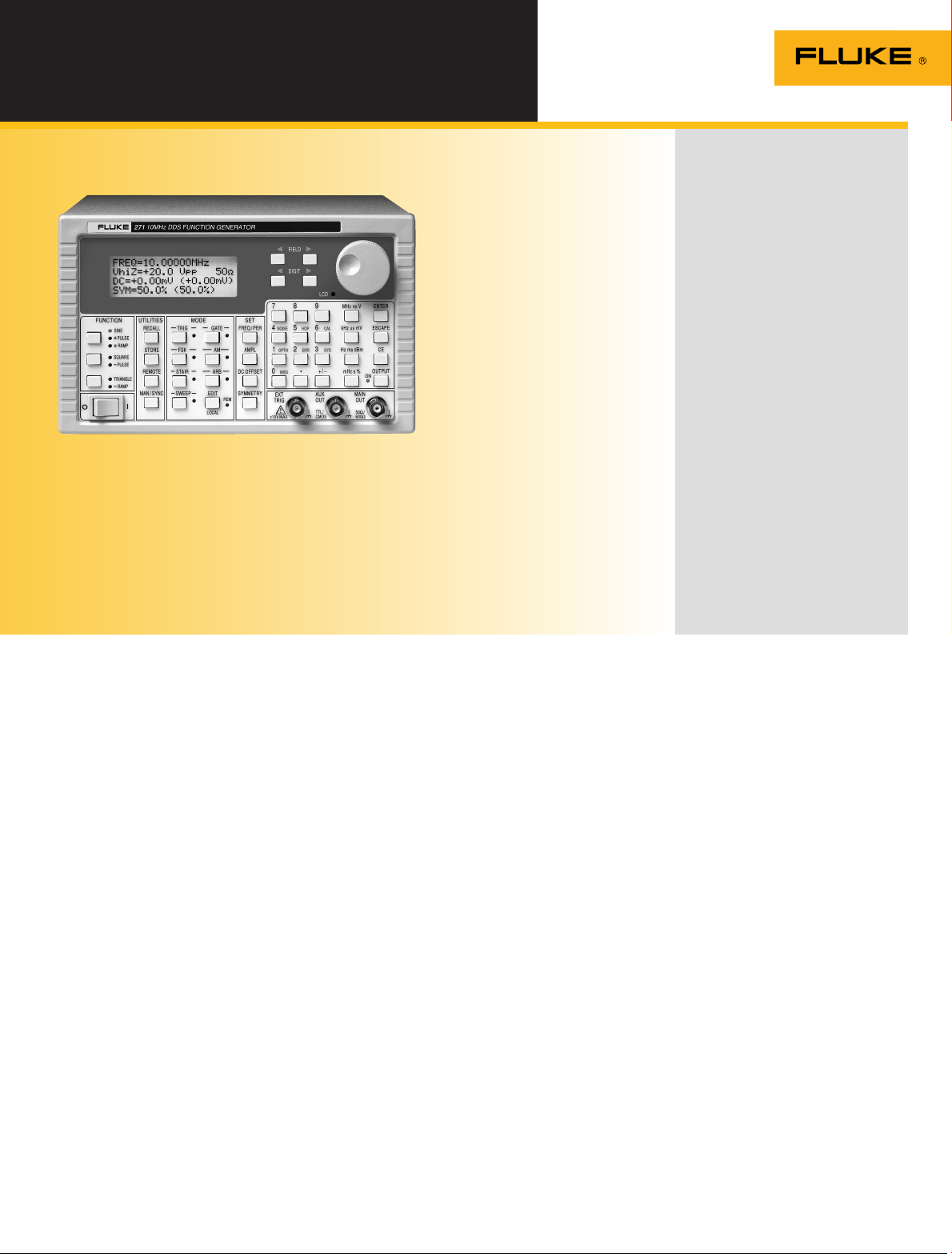
The 271 is a high performance function generator using
Direct Digital Synthesis techniques. A wide variety of
standard waveforms are provided and an arbitrary
waveform capability allows it to be used to generate
non-standard and user-defined waveforms. Extensive
modulation capabilities make this a highly versatile
signal source.
Waveforms
Standard waveforms are sine, square, positive pulse,
negative pulse, triangle, ramp up, ramp down. Additionally arbitrary waveforms, multi-level squarewaves,
waveform hopping and pseudo-random noise can be
generated.
Signal Sources
225
Page 2
271 DDS Function
Generator with ARB
Function Generators
Waveforms
Frequency
All waveforms are available up to 10 MHz. However, the purity of triangle, ramp, and multi-level square wave waveforms is not specified
ove the frequencies indicated in the following section.
ab
Range 0.1 mHz to 10 MHz
Resolution
Accuracy Typically < ± 10 ppm for 1 year, 18 °C to 28 °C
empco. Typically < 1 ppm/°C outside 18 °C to 28 °C
T
Sinewave
Distortion < –60 dBc to 20 kHz, < –50 dBc to 300 kHz, < -35 dBc to 10 MHz
Spurii
Squarewave
Rise and fall times < 22 ns
Triangle
inearity error < 0.5 % to 30 kHz
L
Positive and Negative Ramp
inearity error < 0.5 % to 30 kHz
L
Positive and Negative Pulse
Rise and fall times < 22 ns
Multi-Level Squarewave
6 steps available per cycle, each step selectable for amplitude (10 bit resolution) and duration (1 to 1024 samples). Above 27 kHz a
Up to 1
36 ns edge unc
Rise and fall times < 22 ns
Arbitrary (and complex)
A numb
interfac
they are sampled.
No. of samples 1024 10 bit samples
Noise Wideband noise with variable amplitude and offset.
Symmetry
Range Sine — 1 % to 99 % at all frequencies; Other waveforms — 1 % to 99 % to 30 kHz,
Resolution 0.1 %
ertainty is introduced.
er of “complex” waveforms are pre-programmed in ROM . A further five, user defined, waveforms may be loaded via the digital
es and stored in non-volatile RAM. Frequency range: All waveform points can be continuously output up to 27 kHz, beyond which
7 digits or 0.1 mHz
Non -harmonically related spurii typically <- 60 dBc to 10 MHz
20 % to 80 % to 10 MHz
Main Output
Output impedance 50 Ω or 600 Ω switchable
Amplitude 5 mV to 20 V pk-pk open circuit (2.5 mV to 10 V into 50
(open circuit value) or V (Voltage into the characteristic impedance) in pk-pk, RMS or dBm. Note that in
positive or negative pulse modes the amplitude range is 2.5 mV to 10 V pk-pk O/C.
Accuracy Typically ±3 % ±1 mV at 1 kHz into 50 Ω/600 Ω
Flatness ±0.2 dB to 500 kHz; ±1 dB to 10 MHz
Pulse aberrations <5 %+ 2 mV
DC offset ± 10 V from 50 Ω/600 Ω offset plus signal peak limited to ± 10 V from 50 Ω/600 Ω
Resolution 3 digits or 1 mV for both amplitude and offset
Ω/600 Ω). Output can be specified as V-H: 2
Modulation
Amplitude Modulation
Carrier frequency 0.1 mHz to 10 MHz
Carrier waveforms All
Depth 0 to 100 %, resolution 1 %
Internal source 1 kHz fixed sinewave or 0.005 Hz to 50 kHz square wave
External See “VCA In” section
Frequency Shift Keying (FSK)
Phase coherent switching between two frequencies at a rate defined by the switching signal source
Carrier frequency 0.1 mHz to 10 MHz
Carrier waveforms All
Switch repetition rate dc to 50 kHz internal, dc to 1 MHz external
Switching signal source Internal from keyboard or trigger generator. External from EXT TRIG input or remote interface.
226 Signal Sources
Page 3

Operating Modes
Trigger/burst
Phase coherent signal keying — each positive edge of the trigger signal will produce one burst of the carrier, starting and stopping at the
phase angle specified by the start/stop phase setting
Carrier frequenc
Carrier waveforms All
er of cycles 1 to 1023 (resolution 1 cycle) or 0.5 to 511.5 (resolution 1/2 cycle)
Numb
Trigger rep
e Internal from keyboard or trigger generator. External from EXT TRIG input or remote interface
Sourc
Gated
Non phase-coherent signal keying — output is On while Gate signal is high and Off while low.
Carrier frequenc
Carrier waveforms All
Trigger rep
Gate source Internal from keyboard or trigger generator. External from EXT TRIG input or remote interface
Sweep
Carrier wa
Sweep mode Linear or logarithmic, single or continuous
Sweep w
Sweep time 10 ms to 999 s (3 digit resolution)
Markers
Sweep trigger source The sweep may b
Hop
Up to 16 different “hop” waveforms can be defined in terms of function, frequency, amplitude, offset and duration. Duration setable per
step 1 ms to 60 s.
Start/Stop Phase
Carrier frequency: 0.1 mHz to at least 1 MHz
Carrier waveforms All
Range –360 to +360 degrees
Resolution 1 degree
Accuracy Typically 1 degree to 30 kHz
Trigger Generator
Internal source 0.005 Hz to 50 kHz squarewave adjustable in 20 us steps. 3 digit resolution. Available for external use from TRIG/SWEEP OUT
socket.
y 0.1 mHz to 10 MHz
. rate dc to 50 kHz internal, dc to 1 MHz external
y From 0.1 mHz to 10 MHz
. rate dc to 50 kHz internal dc to 1 MHz external
veforms All
idth 0.1 mHz to 10 MHz. Phase continuous. Independent setting of the start and stop frequency.
Two markers variable during sweep. Available at the TRIG/SWEEP OUT socket
e free run or triggered from: keyboard, EXT TRIG input, remote interface
Auxiliary Outputs
Aux Out
CMOS/TTL levels with symmetry and frequency of main output and phase of start-stop phase setting
rig/Sweep Out
T
Multi-function output depending upon mode. Exc
In Sweep mode the output is a 3-level wa
each marker point
.
ept in sweep mode, the output is that of the trigger generator at C
veform, chang
ing from high (+4 V) to low (0 V) at the start of sweep, w
Inputs
rig
Ext T
y range
Frequenc
nal range
Sig
idth 50 ns
. pulse w
Min
VCA In
Frequency range DC - 100 kHz
Signal range 2.5 V for 100 % level change at maximum output
Input impedanc
e Typically 6 k
DC to 1 MHz
TTL (1.5 V) threshold; maximum input ± 10 V
Ω
/TTL levels from 1 k
S
O
M
ith narrow 1 V pulses at
Ω.
Signal Sources 227
Page 4

271 DDS Function
Generator with ARB
Function Generators
Phase Locking
Clock in/out
Sync out TTL/CMOS logic levels from typically 50
TTL/CMOS threshold levels; output impedance typically 50
Ω. The signals from these sockets are used to phase lock two or
more generators.
Ω as an output
Interfaces
S-232 Variable Baud rate, 9600 Baud maximum. 9-pin D-connector.
R
IEEE-488 Conforming with IEEE488.1 and IEEE488.2
General
y 20 character x 4 row alphanumeric LCD
Displa
Data entry Keyboard selection of mode, waveform etc.; value entry direct by numeric keys or by rotary control.
Stored settings
Size 3U (130 mm) height; half-rack (212 mm) width, 330 mm long
eight 4.1 kg (9 lb)
W
ower 100 V ac, 110 to 120 V ac or 220 to 240 V ac +/– 10 %, 50/60 Hz ac by internal adjustment; 30 VA max.
P
Operating range
Storage range
Options
Up to 9 complete instrument set-ups may be stored and recalled from battery-backed memory.
°C to 40 °C, 20 to 80 % RH
+5
–20 °C to +60 °C
IEEE-488 interface; 19-in rack mounting kit
228 Signal Sources
Ordering Information
Models
271 10 MHz DDS Function
Generator with Serial Cable
Options and
Accessories
1
0
Y28
7
2
1 Rack
mount Kit
 Loading...