

Service Manual
/ ON
LAST MEMO
RETURNON SCREEN A-B REPEAT
TV CH+ TV VOL+
TV POWER
P
U
T
E
S
SHIFT
ENTER
T
REV
I
T
L
SLOW
E
R
E
V
P
L
P
R
E
V
P
A
U
S
E
/
S
T
E
P
213
ANGLE A.REPLAY ZOOM
546
AUDIO
BOOKMARK
879
0
PROGRAM
SURROUND
BASS
-
REMOTE CONTROLLER RB-H5201ST
REPEAT
TV VOL-TV CH-TV/VIDEO
M
E
N
U
PICTURE
MODE
SEARCH
MODE
E
FWD
L
T
I
SLOW
T
B
U
S
D
W
F
Y
A
T
X
E
N
P
O
T
S
SLEEP
C
FUNCTION
SOUND
VOLUME
+
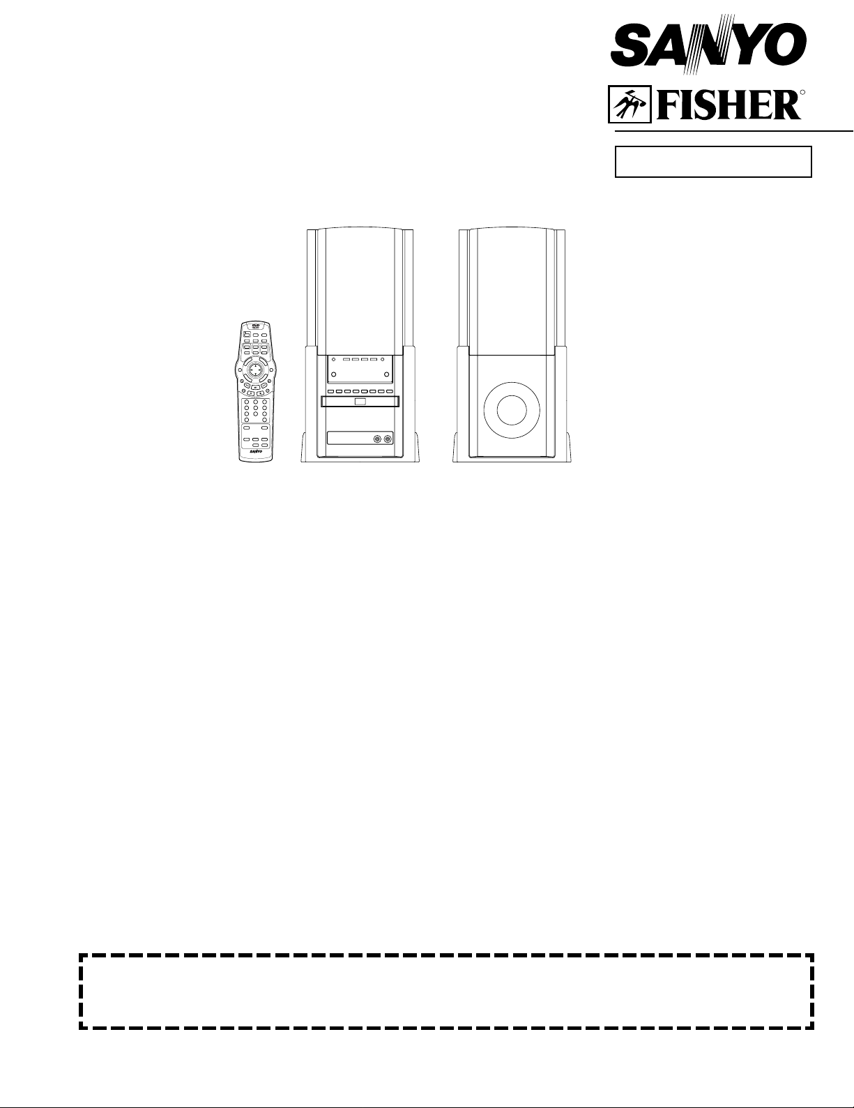
DVD Home Theater System
CONTENTS
Specifications .............................................................................. 1
Laser beam safety precaution.....................................................2
DVD mechanism replacement .................................................... 2
Removal & Installation ................................................................ 3
Mechanism replacement............................................................. 4
Mechanism operation..................................................................5
DVD P.W.Board operation .......................................................... 6
DVD P.W.Board operation
(Schematic diagram for signal check)......................................... 8
DVD P.W.Board operation
(Wiring diagram for signal check) ............................................... 18
DVD P.W.Board operation(Signal)..............................................20
DVD start-up program flow chart ................................................ 28
How to load software for MPEG P.W.Board ............................... 30
MPEG and FRONT END
P.W.Board operation (Block diagram) ...................................... 30
MPEG P.W.Board operation
(schematic diagram for waveform check) ................................... 32
MPEG and FRONT END
P.W.Board check waveform......................................................34
Trouble shooting ......................................................................... 41
Voltage of IC & Transistor ........................................................... 44
Exploded view (Cabinet & Chassis)........................................... 47
Parts list ...................................................................................... 48
Parts list & Exploded view (SP box)............................................57
Exploded view (DVD mechanism) ............................................. 58
IC Block diagram & description ................................................... 59
Memo .......................................................................................... 73
Schematic Diagram (MPEG)......................................................74
FILE NO.
DWM-1000
HTD-5201
PRODUCT CODE No.
129 590 00 (1000)
129 590 01 (XE)
129 590 02 (UK)
129 590 03 (SS)
129 590 04 (KR)
129 590 05 (US)
129 590 06 (CA)
129 590 07 (AU)
Wiring Diagram (MPEG A SIDE) ............................................... 76
Wiring Diagram (MPEG B SIDE) ............................................... 78
Schematic Diagram (AMP for 1000,US,CA) .............................. 80
Wiring Diagram (Pre AMP,Power AMP,Video AMP,
Socket-A for 1000,US,CA) ........................................................ 82
Schematic Diagram (AMP for XE,UK) ....................................... 86
Wiring Diagram (Pre AMP,Power AMP,Video AMP,
Socket-A for XE,UK) ................................................................. 88
Schematic Diagram (AMP for SS) ............................................. 92
Wiring Diagram (Pre AMP,Power AMP,Video AMP,
Socket-A for SS) ....................................................................... 94
Schematic Diagram (AMP for KR) ............................................. 98
Wiring Diagram (Socket-A for KR) .............................................. 100
Wiring Diagram (Regulator & Digital Out) ................................... 101
Schematic Diagram (AMP for AU) ............................................. 102
Wiring Diagram (Pre AMP,Power AMP,Video AMP,
Socket-A for AU) ....................................................................... 104
Wiring Diagram (Front for 1000,US,CA) .................................... 108
Wiring Diagram (Front for XE,UK) ............................................. 109
Schematic Diagram (Front for 1000,XE,UK,US,CA)................... 110
Schematic Diagram (Front for SS,KR)....................................... 112
Wiring Diagram (Front for SS,KR) .............................................. 114
Wiring Diagram (Front for AU) .................................................... 115
Schematic Diagram (Front for AU).............................................116
Schematic Diagram (DVD).........................................................118
Wiring Diagram (DVD A side) ..................................................... 128
Wiring Diagram (DVD B side) ..................................................... 129
Wiring Connection (1000,US,CA,AU) ......................................... 130
Wiring Connection (XE,UK,SS,KR).............................................Rear
R
(US)
(XE)
(UK)
(SS)
(KR)
(US)
(CA)
(AU)
This service manual consists of "DWM-1000M"[US](Main unit: 129 591 00), "DWM-1000SP"[US](Speaker system: 165 029 00). "HTD-5201M"
[XE](Main unit: 129 591 01), [UK](Main unit: 129 591 02), [SS](Main unit: 129 591 03), [KR](Main unit: 129 591 04), [US](Main unit: 129 591 05),
[CA](Main unit : 129 591 06), [AU](Main unit: 129 591 07), "SX-5201/XE" [XE](Speaker system: 165 029 01), "SX-5201/SS" [UK,SS,KR,AU](Speaker
system: 165 029 02), "STM-5201/US" [US](Speaker system: 165 029 04) and SX-5201/CA[CA](Main unit: 165 029 05).
REFERENCE No.
SM5810205

SPECIFICATIONS
Main unit with Main Speaker
Amplifier Section
<US>
Main Amplifier
Continuous minimum sine wave RMS power output
per channel at 1kHz into 6 ohms with no more than
10 % total harmonic distortion ................ 3 0 W a t t s
Subwoofer Amplifier
Continuous minimum sine wave RMS power output at
100Hz into 6 ohms with no more than 10 % total
harmonic distortion ..................................... 30 Watts
General
Output power
Total power : 90W
Main Amplifier : 30 x 2 (at 6 ohms, 10% distortion)
Subwoofer Amplifier : 30W (st 6 ohms, 10% distortion)
Input level and impedance:
VIDEO: VIDEO IN : 1.0 Vp-p (75 ohms)
AUDIO IN (L/R): 600 mV/50k ohms
AUX/TV (L/R): 600 mV/50k ohms
Outputs:
MAIN SPEAKER (L/R): 6 ohms
SUBWOOFER: 6 ohms
PHONES:8-32 ohms (XE,UK,SS,KR,AU)
DIGITAL OUT: Optical
AV EURO CONNECTOR : For Euro-AV cable (XE,UK)
COMPONENT VIDEO OUT: CB/CR: 0.7 Vp-p (75 )
Y: 1.0 Vp-p (75 )
MONITOR VIDEO OUT: 1.0 Vp-p (75 ohms)
AUDIO OUT (L/R): 600 mV (1 kohms)
S-VIDEO OUT: Y: 1.0 Vp-p (75 ohms)NTSC
Y: 1.0 Vp-p (75 ohms)PAL
C: 0.286 Vp-p (75 ohms)NTSC
C: 0.3Vp-p (75 ohms)PAL
Main Speaker (magnetic shield)
Unit used: 10cm ( 4" diameter), Cone type
Maximum music power handling capacity: 60 Watts
Nominal impedance: 6 ohms
General
Power requirements: AC 120V, 60Hz (1000,US,CA)
AC 230V, 50Hz (XE,UK)
AC 230-240V,50Hz (AU)
AC 220V, 60Hz (KR)
Power consumption: 100 Watts
1.4W (standby mode)
Dimensions (W x H x D):Approx. 200(W) x 400(H) x 320(D) mm
Approx. 7.9" x 15.9" x 12.6"
Weight: :Approx.8.7 kg (19.4 lbs)
Main Speaker with Subwoofer (magnetic shield)
Main Speaker
Unit used: 10cm (4" diameter), Cone type
Maximum music power handling capacity: 60 Watts(peak)
Nominal impedance: 6 ohms
Subwoofer
Unit used: 13cm ( 5.1" diameter), Cone type
Maximum music power handling capacity: 60 Watts (peak)
Nominal impedance: 6 ohms
General
Dimensions (W x H x D): Approx 200(W) x 400(H) x 320(D) mm
Approx. 7.9" x 15.9" x 12.6"
Weight: Approx. 5.8 kg (13.2 lbs)
IMPORTANT INFORMATION
Because its products are subject to continuous improvement,
SANYO reserves the right to modify product designs and
specifications without notice and without incurring any obligation.
Specifications subject to change without notice.
DVD Video Player Section
Type: DVD/CD player
Playback standard : PAL or NTSC
Laser: Semiconductor laser, wavelength 650 nm
Laser output (Continuous wave max.)
1mW (DVD)
0.5mW (CD)
Frequency range (digital audio):
4 Hz to 44 kHz (DVD fs: 96 kHz)
Signal to noise ratio: More than 105 dB
Harmonic distortion (digital audio): 0.003 %
Wow and flutter: Below measurable level
- 1 -
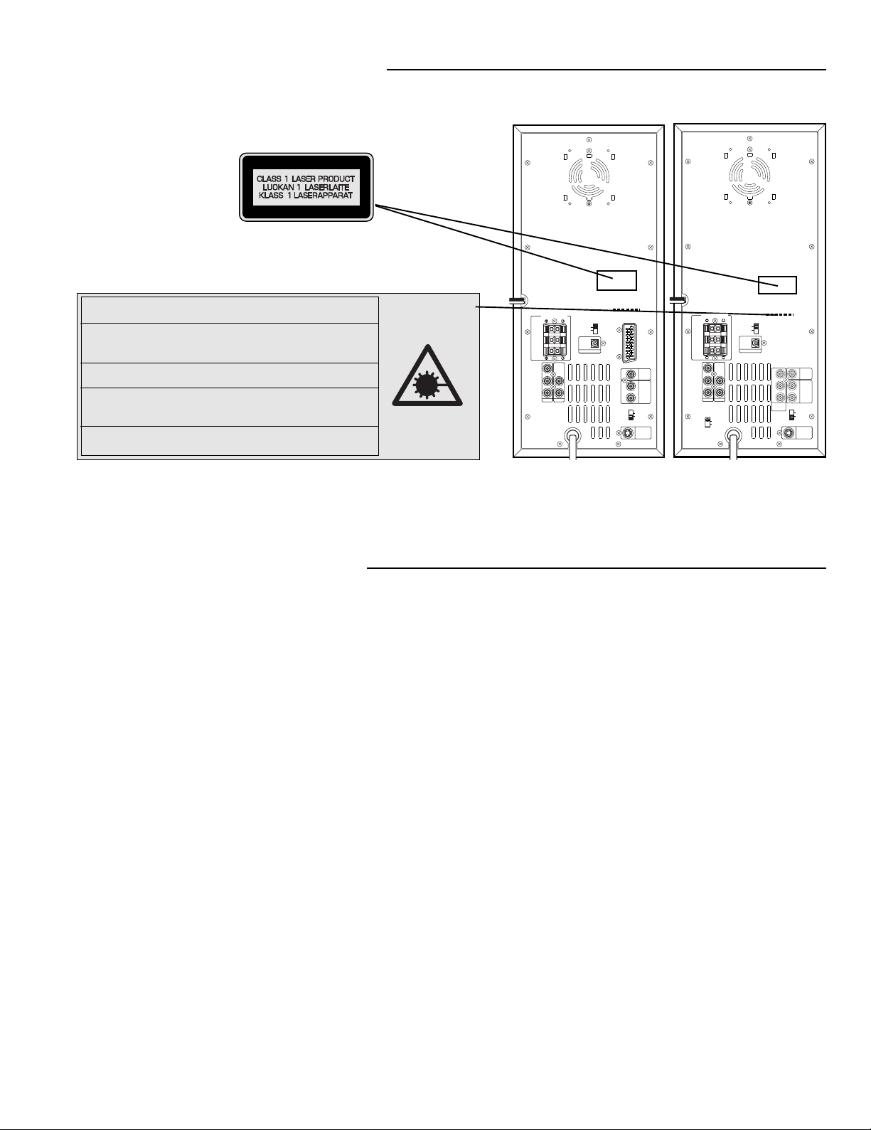
LASER BEAM SAFETY PRECAUTION
SUB
WOOFER
VIDEO IN
AUDIO IN
VIDEO OUT SELECT
RGB
S-VIDEO
S-VIDEO OUT
(DVD ONLY)
MONITOR
VIDEO OUT
AUDIO OUT
R
L
R
VIDEO
AUX/TV
LRL
R
L
OPTICAL
DIGITAL OUT
TV SYSTEM
AV EURO
CONNECTOR
(RGB OUT)
PAL
NTSC
SPEAKERS(6ΩMIN.)
XE,UK,SS,AU
XE,SS
CAUTION – INVISIBLE LASER RADIATION WHEN OPEN AND
INTERLOCKS DEFEATED. AVOID EXPOSURE TO BEAM.
ADVARSEL – USYNLIG LASER STRÅLING VED ÅBNING, NÅR
SIKKERHEDSAFBRYDERE ER UDE AF FUNKTION, UNDGÅ UDS ÆTTELSE
FOR STRÅLING.
VARNING – OSYNLIG LASER STRÅLNING NÄR DENNA DEL ÄR ÖPPNAD
OCH SPÄRR ÄR URKOPPLAD. STRÅLEN ÄR FARLIG.
VORSICHT – UNSICHTBARE LASERSTRAHLUNG TRITT AUS, WENN
DECKEL GEÖFFNET UND WENN SICHERHEITSVERRIEGELUNG
ÜBERBRÜCKT IST. NICHT, DEM STRAHL AUSSETZEN.
VARO – AVATTAESSA JA SUOJALUKITUS OHITETTAESSA OLET ALTTIINA
NÄKYMÄTTÖMÄLLE LASERSÄTEILYLLE. ÄLÄ KATSO SÄTEESEEN.
DVD MECHANISM REPLACEMENT
1. Cautionary instructions in handling the assy
(Safety instructions)
Optical pickup
The laser beam used in the pickup is classified as "class 2". Exposing
your eyes or skin to the beam is harmful. Take care not to do so.
(Caution against static electricity and leakage voltage)
Ground securely the work tables, tools, fixtures, soldering irons
(including those made of ceramic) and measuring instruments used
in the production lines and inspection departments that handle
loaders. The workers shall also be grounded.
(Cautionary instructions in handling)
Do not touch the object lens when handling a loader, or the lens
will be stained, resulting in inadequate playability.
There is no power supply protection circuit provided for this product
or adjustment/inspection device. Short-circuiting may lead to fire or
damage.
Take care so as to protect from exposure to water, the entry of
metallic pieces or dew condensation.
In particular, a strong magnet adjacent to the pickup will not only
get inoperative but can damage the pickup if a small metallic piece,
such as a screw or swarm, enters.
The loader edge can cause injury if inadvertently handled.
Do not touch a rotating disk, or injury may result.
This product is a precision device. Handle carefully.
A shock or dropping will cause misalignment or destruction. If it
should occur, refer to clause 2.
This product is so designed as to endure an initial shock equivalent
to a drop from a height of approx. 90 cm under the packed condition.
After the initial shock, the resistivity will still remain at a level of 50
to 60 G, but the mechanical robustness
The entry and deposition of dirt into or on the pickup lens or moving
section will cause malfunction or degradation.
SPEAKERS(6ΩMIN.)
TV SYSTEM
L
R
SUB
WOOFER
VIDEO IN
LRL
AUDIO IN
R
VOLTAGE SELECTOR
PAL
NTSC
OPTICAL
DIGITAL OUT
C
R
C
B
VIDEO
AUX/TV
230V
115V
COMPONENT
VIDEO OUT
(DVD ONLY)
XE,UK SS,AU
(Connectors)
Do not connect or disconnect while power is on.
Connecting or disconnecting signal wires or the main power cord
when the power is on may destruct the unit or fixture.
When connecting, push all the way in securely.
An insufficient insertion may cause a bad contact, leading to an
erroneous operation.
Do not connect or disconnect roughly by an excessively strong force,
or a broken wire or bad contact may result.
Semiconductors are connected. Do not touch connector terminals
directly.
If the worker is grounded, there is nothing to worry about static
electricity, but the rust on the connector terminal surface caused
by the touch may result in bad contact.
(Power source)
The power source need be good in quality (free from instantaneous
interruptions or noises).
A low quality power source may well cause malfunction.
(Storage)
Do not place or store in a dusty place or a place where dew
condensation is possible.
The entry and deposition of dirt or dust into or on the pickup lens or
moving section will cause malfunction or degradation.
Also, dew condensation causes rust ; the rust penetrate into the
precision part of a pickup, causing malfunction, or degrading the
optical quality of the internal lens and reflector, which also leads to
malfunction.
- 2 -
MONITOR
VIDEO OUT
AUDIO OUT
RLY
VIDEO OUT SELECT
COMPONENT
S-VIDEO
S-VIDEO OUT
(DVD ONLY)
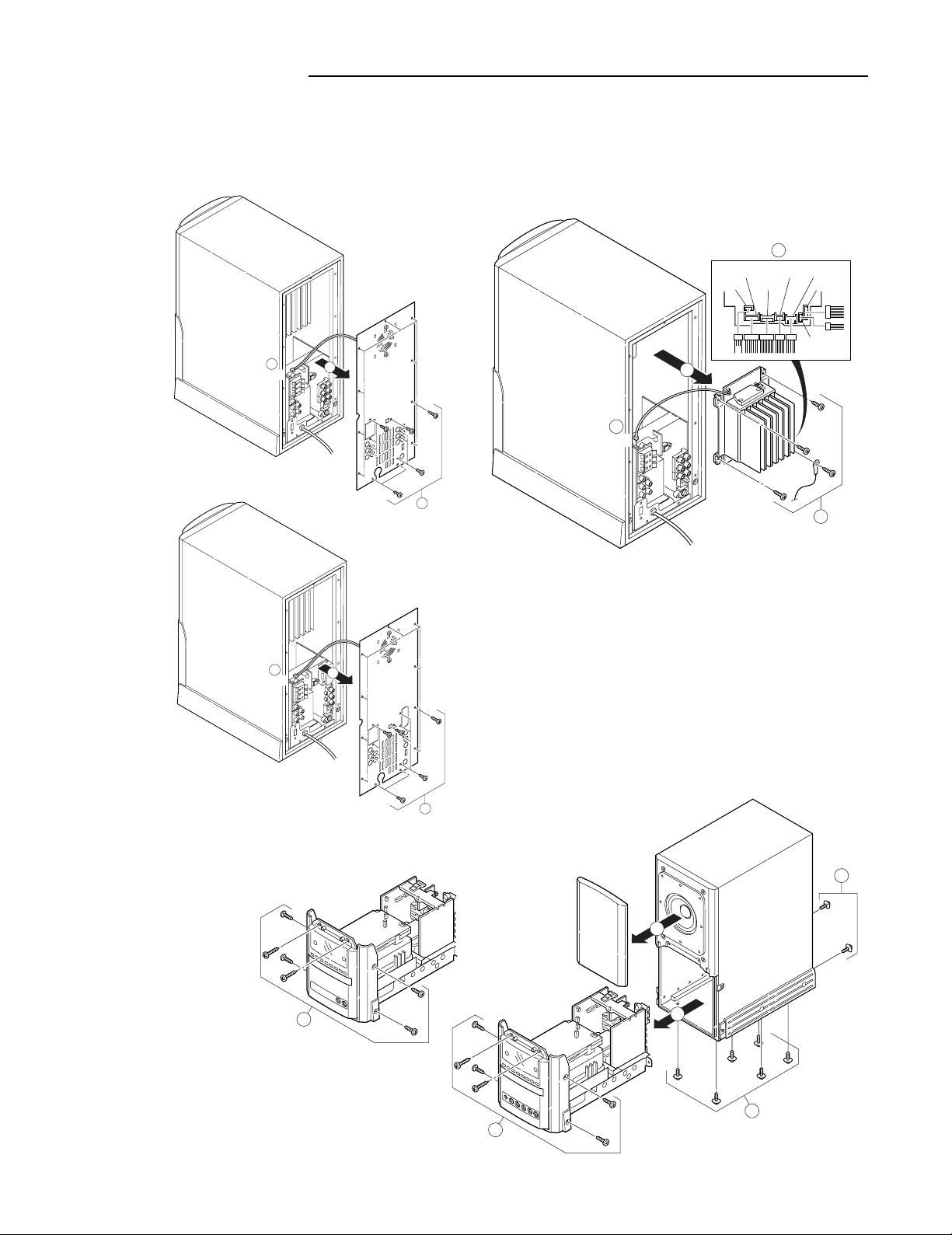
REMOVAL & INSTALLATION
Remove the power supply cord from AC outlet.
All wiring should be returned to the original position after work is completed.
Check and maintenance can do, if operate the following order.
1. Removal Rear Panel 2. Removal Power supply P.W.B.
3
CN439
2
4
CN438
2
CN472
CN471
3
CN475 CN477
CN476
CN470
CN474
UK,XE only
3. Removal Front grill Block
3
CN439
1
1
2
1
3
1
4
1000,XE,UK,US,CA,AU
5
2
4
SS,KR
- 3 -
MECHANISM REPLACEMENT
FLOIL OIL
G-2000B
FLOIL OIL
G-2000B
1. TRAY and BASE MechanismPart
FLOIL OIL
G-474B
3. TRAY Part
MOLYKOTE
EM-50L
GREASE
CDF-409
GREASE
CDF-409
2. BASE Mechanism Mounting Part
SILICON GREASE
KS-64
MOLYKOTE
EM-50L
MOLYKOTE
EM-50L
4. BASE Mechanism Part
MOLYKOTE
EM-50L
MOLYKOTE
EM-50L
Do not remove the pick-up from base mechanism because of
adjustment difficulty.
- 4 -
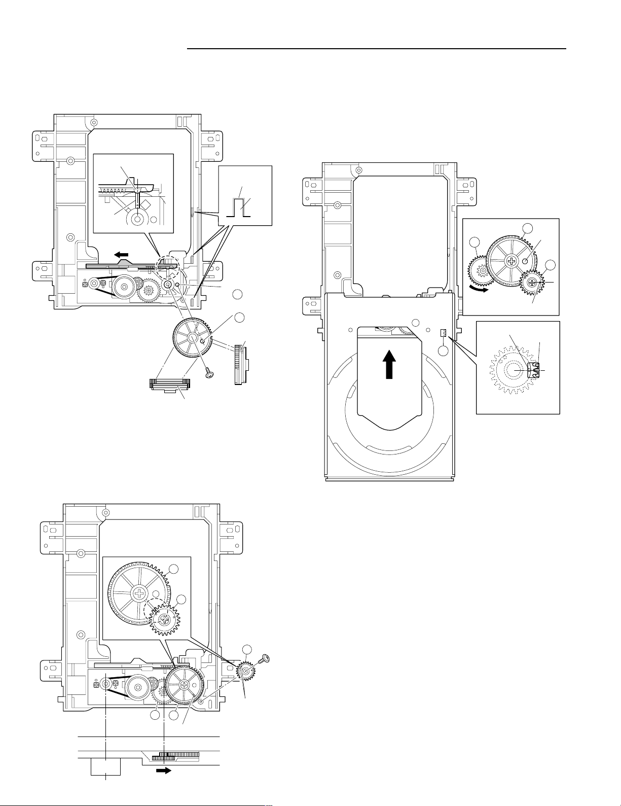
MECHANISM OPERATION
1.How to setting the TRAY
1. Move the SLIDE left side.
2. Match the Hole of GEAR
LARGE TOOTH
5 and Hole of CHASSIS 4.
GREASE
EM-50L
RIB
6. Match the hole of GEAR 7 and hole of chassis while turning
GEAR 6.
7. Match the mark of LOADING GEAR
8 and gear of TRAY
where see horn hole 9 of tray.
8. Push a TRAY with the state that turned the entire surface of a
TRAY into approximately 5 degrees the lower part slowly.
RIB
CHASSIS HOLE
4
GEAR HOLE
5
GREASE
EM-50L
GREASE
EM-50L
3. Match the mark of GEAR 2 and mark of GEAR 3, and then
install the BOSS.
4. Turn the GEAR
1 counterclockwise, and then SLIDE move
right side.
5. The GEAR
1 move from side to side.
TRAY
7
6
HOLE
8
MARKER
MARKER
LOARDING
GEAR
9
MOTOR
CHASSIS
FRONT SIDE
3
2
2
MARKER
1
3
MARKER
- 5 -

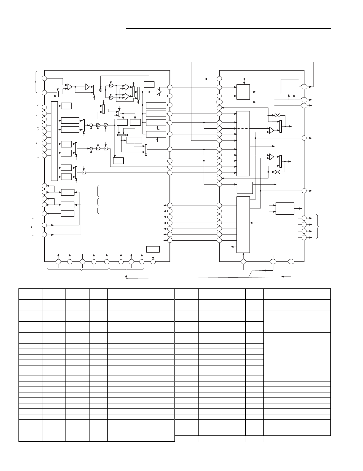
DVD P.W.BOARD OPERATION
1. General operation diagram ( This is a basic general operation diagram)
The circuit mounted on the Loader part (Frontend Board) is configured as shown, which is divided into following bl;ocks according to
main IC's.
DVD/CD PD
LASER
DIODE
ACTUATOR
SLED
MOTOR
LIMIT
SWITCH
OPEN/CLOSE
SWITCH
LOADING
MOTOR
PICK-UP;SF-HD6
High-
frequency
circuit
FOCUS
TRACKING
M
M
SPINDLE
MOTOR
HALL
LD
VR-CD
VR-DVD
MD
LD-CD
VD
HFM
D
GND-LD
VREF
LSI_RESET
HDAT[0;7]
DSPJVAD
16.934MHZ
3.3V
(FOR DSP)
DACK
DREQ
DCLK,DBGN,DERR
SDT[O;7]
EMPH,C2F,LRCK,BCK,CD_DATA,SPDIF
16MHZ
HADR[0;12]
HRDB,HERB,HCSB
HWAITB(RDY),HBUSYB
HIRQB(INT_DEC),WRQ
LE28C1001
FLASH MEMORY
RXD,SCLK
HD_INT,TXD,RDY_HIF
RESET HRST
16MHZ
IC201
T224162B
DRAM
IC900
BA033
REGULATOR
IC504
TC7SHU04FU
INVERTER
IC550
IC502
M51953
RESET
9V
(actuator)
(motor)
5V
(analog)
5Vd
(digital)
PH 6P
FFC 26P
FFC 16P
TO BACK-END
BLOCK
CN900CN200CN500
RF AMP
A
B
C
D
E
F
F-
F+
T-
T+
MD
LD
MD
LD
5Vd
CAO
U+,UV+,VW+,W- SPD
U,V,W
IC100
LA9702
CAN
LDON1,LDON2
CD x2
RFSCT,EQSCT
CD x4
PP/TE,DPD/TE
4-CH BTL DRIVER
IC601
BA5937
DMUTE2
3-PHASE MOTOR DRIVER
IC602
BA6849
9V
FDD
TDD
SLD
OPEN/
CLOSE
9V
FG
FR
DMUTE
TOST,FOST,BST,VCA
TBAL,FBAL,SGC
DEF
FE
RFOP,RFON,PH,TE,ADBH
ADBH
DEF_INH
DEFECTO
XHTR
IC101
BU4066
ANALOG SWITCH
JV
BH
DEFECTI
M37903S4CHP
FE
IC500
IC200
LC78661W
MICRO COMPUTER
- 6 -
DVD P.W.BOARD OPERATION
1
2
3
4
5
6
7
8
9
10
11
14
13
16
15
79
72
70
76 61 68 63 59 53 27
18
19
20
21
22
23
24
35
34
33
32
31
30
29
1
2
10
14
7
6
13
9
8
5
28
29
32
45
41
40
46
44
42 12
18
16
206
44
26
154
134
136
28
39
27
38
37
36
20120525
11
30
5157
XHTRC
DEFECT0
RFP1
TH
TESBIAS
HFLBIAS
HFLBIAS
TESBIAS
TES
HFL
PCK
PCK
JV
JITTER
DETECTION
CIRCUIT
SLCBIAS
LDO1
LDS1
LDO2
LDS2
SLC
SLCBIAS
EFMINP
EFMINN
DEFECTI
HFLIO
RF-PH
RF-BH
AD5/BH
AD2
AD1
TE
AD4/TE
AD3
FE
AD0
TESIO
EFMOUT
EFM,EFM+
EFM+
EFM
DEFECT
FE,TE,PH,BH,RPEC,
JV,BCA,WO
DEGITAL.
CLK
COUNTER
FDO
TDO
SPDO
SLDO
CPOF
VREF
SLCBIAS
SGC
OFSET
BCA
BOOT3T
RFVCA
TBAL
FBAL
D/A
8bit
11ch
+3ch
D/A
8bit
10ch
TES
WO-CNT
HFL
TRACK
COUNTER
DEGITAL.
OFSET,BCA,BOOT3T,
RFVCA,TBAL,FBAL,
SGC,HFLBIAS,TESBIAS,
FDO,TDO,SPDO,SLDO,
SLCBTAS.
RFPI
RFOP
RFON
DEF
PH
BH
BCA
TE
WO
FE
RREC
TOST
FOST
BST
VGA
TEBL
FEBL
SGC
SERVO
VREFS
VREFS
TH
CPOF
XHTRC
DPD/TE
XQBHPP/TEEQSCT
RFSCT
VREFP
LDON1
LDON2
PICK
APC1
RR 1
B
FE 1
FE 2
RR 2
APC2
VREFP1
MTX
A
D
C
C
A
DVD
PU
DVD
PU
B
F
E
DPD
2C+A+B
3-BEAM
PUSH-PULL
REN
REP
LPF
BCA TH
DEFECT
PEAK HOLD
BOTOM HOLD
TE HOLD
LPF2LPF1
BPF
DPD: PHASE A,B,C,D
3-BEAM: F~E
PUSH-PULL: (B+C)-(A+D)
FE1: (B+D)-(A+C)
FE2: A-B
RR1: A+B+C+D
RR2: A+C+B
TE
FE
RREC
RFSCT
CD-3T
BOOST
DPD / TE
VGA
BST
DPD / TE
EQ2
EQ1
EQSCT
CPOF OR TH
DPD / TE
VREF
XHTRC
XHTRC
PP / TE
TOST
FOST
TE
FE
SGC
SGC
SGC
RFSCT
RFSCT
TH
BCATH
CD
PU
MI-COM
PORT
MI-COM PORT DSP CONTROL
to
DRIVE
IC
LA9702W(AMP) LC78661W(DSP)
IC100
IC200
2. Circuit configuration inside IC100 (LA9702W) and IC200 (LC78661W).
(This is a basic circuit configuration diagram)
Name TP label
FE TP101 IC100 25 Focus Error Signal(Analog) TD TP601 IC200 3 8 Tracking Driver out(analog)
TE TP102 IC100 30 Tracking Error Signal(Analog) FD TP602 IC2 00 39 Focus Driver out(analog)
RFN TP104 IC100 4 0 RF Signal(Analog) SPD-FG TP604 IC 602 24 Spindle FG signal
RFP TP105 IC100 41 RF Signal(Analog) W TP621 ------ ------
BH TP106 IC100 42 Bottom Hold Signal(Analog) V TP620 ------ ------
PH TP107 IC100 44 Peak Hold Signal(Analog) U TP611 ------ -----DEF TP230 IC100 46 High : When passing defection H+ TP619 ------ -----LD1 TP122 Q1004 E DVD Laser Power Supply(Analog) U+ TP618 ------ -----LD2 TP124 Q1005 E CD Laser Power Supply(analog) U- TP617 ------ ------
TESI0 TP201 IC200 2 TES(Track crossing signal) V+ TP616 ------ ------
HFLBIAS TP204 IC200 2 8 MIRROR Slice Bias(Analog) V- TP615 ------ ------
HFLIO TP206 IC200 44 MIRROR signal W+ TP614 ------ ------
FSEQ TP211 IC200 8 4
EFMOUT TP226 IC200 134 RF Digitized signal H- TP612 ------ ------
DEFECT0 TP229 IC200 201 High : When passing defection SLD TP607 I C200 36 Sled Driver out(analog)
TOST TP246 IC200 29 Tracking Offset Control(analog) SPD TP608 IC200 3 7 Spindle Driver out(analog)
FOST TP247 IC200 30 Focus Offset Control(analog) OPEN ------ I C60 1 1 6 TRAY control signal
BOOST3T TP248 IC200 3 1 RF EQ Control(analog) CLOSE ------ IC601 15 TRAY control signal
RFVCA TP249 IC200 32 RF Voltage Control(analog) OPEN-SW TP627 CN600 5 TRAY Limit SW
TBAL TP250 IC200 33 Tracking Balance Control(analog) CLOSE-SW TP626 CN600 3 TRAY Limit SW
FBAL TP251 IC200 34 Focus Balance Control(analog) HRST TP700 CN500 2 RESET from Backend
SGC TP252 IC200 35 Signal Gain Control(anlog) RESET ------ IC502 6 RESET to Micom
HFBUSYB TP254 IC200 50
IC, CN
Location Pin no. Description Name TP label
JVAO TP257 IC200 154 Jitters value(analog)
High : Sync synchronised
LO : Async W- TP613 ------ ------
Function Busy Low during jump,
adjustment so on.
IC, CN
Location Pin no. Description
VREF ------ IC100 27, 79 Reference Voltage(2.5V)
Spindle Coil Voltage
Spindle Hall Voltage
- 7 -
TROUBLE SHOOTING
(This is a basic trouble shooting.)
General flow
XE,UK Version
AC-CORD PLUG IN
Except XE,UK Version
POWER SUPPLY.FSTANDBY mode
IC601 ACTIVE/P-CON.FLOW
+5V/+12/-30/FIL.FOFF
STANDBY LED LIGHT
OK
POWER KEY
PRESS
P-CON.FHIGH
+5V/+12/-30/FIL.FON
OPEN/CLOSE.ETRAY LED LIGHT
IC601 STANDBY DATA WAITE
STANDBY LED OFF
OK
RESET LOADER AND
CHIPS
OK
READ/WRITE DATA
IN EEPROM
START
COMMUNICATION
WITH VFD
FROM MPU STANBY DATA SEND
IC601 STANDBY DATA RCVD
IC601 POWER ON DATA SEND
OK
NG
IC601 VDD/RESET/OSC confirm
NG
IC601:FPC16316-80 confirm
STANDBY LED peripheral circuit confirm
P-COn/+5V/+12/-30/FIL confirm
POWER KEY confirm
NG
LED peripheral circuit confirm
P-CON/+5V/+12/-30/FIL confirm
RESET (IC130) confirm
VDD/CLOCK confirm
IC116 peripheral confirm
NG
Communication LINE confirm
REMCON NG. IC116/IC113,112
l
periphera confirm
REMCON OK. then IC601
peripheral confirm
STANDBY LED
LIGHT
OK
POWER KEY
PRESS
STANDBY LED
OFF
OK
OPEN/CLOSE.ETRAY
LED LIGHT
OK
RESET LOADER AND
CHIPS
OK
READ/WRITE DATA
IN EEPROM
START
COMMUNICATION
WITH VFD
VFD
INDICATE
"READING"
OK
NG
NG
NG
IC601 VDD/RESET/OSC confirm
IC601:UPD16311 confirm
STANDBY LED peripheral circuit confirm
POWER KEY confirm
STANDBY LED peripheral circuit confirm
NG
LED peripheral circuit confirm
RESET (IC130) confirm
NG
VDD/CLOCK confirm
IC116 peripheral confirm
IC BUS LINE confirm
IC601 VFD
peripheral circuit confirm
-30V.EFILAMENT voltage confirm
Communication LINE confirm
VFD
INDICATE
"READING"
OK
IC BUS LINE confirm
IC601 VFD peripheral confirm
-30V.EFILAMENT voltage confirm
Communication LINE confirm
NG
VFD
INDICATE
"NO DISC"
- 41 -
INITIALISE
MPEG DECODER
(IC127)
OK
OK
NG
IC118-IC127 BUS-LINE confirm
IC127/116 peripheral confirm
LOADER confirm
NG
Communication LINE confirm (FFC)
PLAYBACK mode
DISPLAY
LOGO
START CONTROL OF
LOADER
PICK INITIALISE
SPINDLE ROTATE
INITIALISE
ADAC(IC130)
DISC Y/NN Y
TROUBLE SHOOTING
(This is a basic trouble shooting.)
AUDIO PART
1. When time display OK and sound NG
or When S/PDIF OK and analogue NG.
Check DAC output
(IC131 pin11/14).
NG
Check (BCLK/
ASDATA/LRCLCIC131
pin 16/17/18).
NG
Check IC127
pin 105/106/107.
NG
Check IC127 peripheral.
(IC127 NG)
OK
OK
OK
Tracking signal of
after DAC output.
Check MUTE signal.
Check IC131 pin1(27MHz)
and pin2(384FS).
Check IC131 power source
and peripheral circuit.
Check IC131 RESET/
control signal(pin6/7/8/9).
Check BCLK/ASDATA/
LRCLK signal line.
Check IC127 and
its peripheral.(IC127 NG)
3. When S/PDIF NG and analogue OK.
Check optical module
and signal line.
NG
Check signal line
peripheralpattern
and parts.
OK
Check IC127 peripheral.
4. When S/PDIF NG and analogue NG.
Check time display.
OK
NG
Check check 2
Check check 1
(IC127 NG)
2. When time display NG and sound NG.
Exchange DVD:Loader.
OK
NG
Check IC127 peripheral.
(IC128 NG)
Check CD:CN810 pin2/3/4.
OK
NG
Exchange loader.
OK
NG
Exchange MPEG
p.w.board.
Loader NG.
Check IC127 peripheral.
(IC127 NG)
Loader NG.
5. When pop noise (when usual operate.)
Check same output as
SPDIF and RCA.
NO
Check pop noise only
RCA output.
NO
IC127 (MPEG) NG.
YES
YES
Loader NG
Muting circuit trouble.
Check MUTE signal.
6. When pop noise (Power ON/OFF).
Specity place of noise
Check MUTE circuit.
(Normality ?)
NO
YES
generation.
Check timing with MUTE
signal and its peripheral.
- 42 -
Check MUTE circuit.
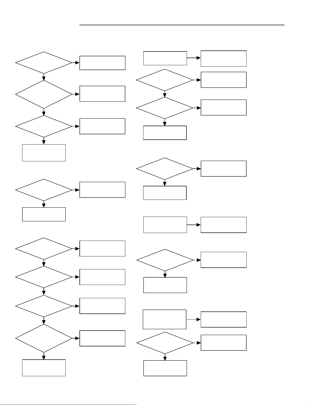
TROUBLE SHOOTING
(This is a basic trouble shooting.)
VIDEO PART
1. When sound OK and picture NG.
4. When confusion of the picture.
Check IC102:video
encorder output.
NG
Check IC102:
video encorder peripheral.
(DVD/reset/pd0-8/
sync/RSET)
NG
Something is wrong
with pd0-8.
NO
Exchange disc
(error rate high).
Inquire the whole.
Check wirng from encorder
OK
OK
TES
output to set output.
IC102 NG.
IC127 NG.
Check wiring.
2. When sound and picture NG and display OK.
Check dac output and
video encorder output.
NG
IC127 NG.
Check the whole.
OK
Inquire wiring.
3. When confusion of the picture.
Color change.
Horizontal/
vertical line enter.
Check video sync.
NG
IC102 video
encorder output.
NG
Check IC102 peripheral.
(IC102 NG)
27MHz oscillating circuit
Check IC127 pin15/16.
OK
Check circuit from IC102
OK
output to set output.
5. When color NG.
27MHz
oscillating circuit trouble.
Check frequency.
NG
Exchange oscillator.
Exchange C8121/C8122.
OK
6. when not change to PAL or NTSC.
Check PAL/NTSC control
line (IC116 pin16 cn671
pin9:high NTSC/low PAL).
Check signal pattern
trouble.
Check frequency.
IC102 NG.
and S6702.
Recover at exchanged
loader.
NO
Recover at exchanged
MPEG p.c.board.
NO
Recover at exchanged
disc.
NG
Check fluctuation
of power source 5V.
Check contact of
connector.
NG
Check power source
p.w.board NG.
Exchange p.w.board.
YES
Check MPEG p.w.board.
YES
OK
OK
Exchange disc.
Check the whole.
Check loader.
7. When s-terminal output NG and color NG.
Check IC102:video
encorder output.
NO
Check solder of
output terminal.
(IC102 NG)
Check circuit from IC102
output to set output.
Check S6701 peripheral.
YES
8. When YUV/RGB NG and color NG.
Check IC102:video
encorder output.
Check S6701 peripheral
circuit.
Check RGB/YUV setting.
NO
Check setting signal
pattern.
(IC102 NG)
Check circuit from IC102
output to set output.
Check S6701 peripheral.
IC102 NG.
YES
- 43 -
VOLTAGE OF IC & TRANSISTOR
V
V
V
V
1. MPEG part
IC101
Pin No. 12345678
Power OFF
Power ON
0V 0V 0V 0V 0.1V 0.1V 0V 0.1V
0V 0V 0V 0V 3.3V 3.3V 0V 3.3V
IC102
Pin No. 12345678910111213141516
Power OFF
Power ON
Pin No. 17 18 19 20 21 22 23 24 25 26 27 28 29 30 31 32
Power OFF
Power ON
Pin No. 33 34 35 36 37 38 39 40 41 42 43 44
Power OFF 0V 0V 0V 0V 0.1V 0.2V 0.1V 0.1V 0.1V 0.1V 0V 0V
Power ON 1.2V 1.2V 0V 0V 3.2V 0.9V 0.9V 0.6V 1.3V 2.5V 0V 1.6V
0.1V 0.1V 0.1V 0.1V 0.1V 0.1V 0.1V 0.1V 0.1V 0V 0.1V 0.1V 0.1V 0.1V 0.1V 0.1V
3.3V 0.8V 0.6V 1.1V 3.3V 3.3V 3.3V 3.3V 3.3V 0V 3.3V 3.3V 3.3V 3.3V 3.3V 3.3V
0.1V 0.1V 0V 0.1V 0V 0.1V 0.1V 0.1V 0V 0V 0V 0.1V 0V 0.1V 0V 0V
2.5V 3.3V 0V 3.3V 0V 3.3V 3.3V 3.3V 1.2V 0.8V 0.8V 3.3V 0V 3.3V 0.7V 0.4V
(V)
(V)
IC103
Pin No. 1 2 3
Power OFF
Power ON
0.6V 0V 0V
5.1V 0V 2.5V
IC104
Pin No. 1 2 3
Power OFF 0.6V 0V 0.1V
Power ON 5.1V 0V 3.3V
(V)
(V)
IC110
Pin No. 12345678910111213141516
Power OFF 0.1V 0V 0V 0V 0V 0V 0.1V 0V 0V 0V 0V 0V 0.1V 0.1V 0.1V 0.1V
Power ON 3.3V --- --- 0V --- --- 3.3V --- --- 0V --- --- 3.3V 0V 3.3V 3V
Pin No. 17 18 19 20 21 22 23 24 25 26 27 28 29 30 31 32
Power OFF 0.1V 0.1V 0.1V 0.1V --- --- 0.5V --- 0.1V 0V --- --- 0V 0V 0.1V 0.1V
Power ON 3.1V 3.1V 0.2V 0V 0 V 0V 0.2V 0.2V 3.3V 0V 0.2V 0.2V 0.2V 0.2V 0V 0V
Pin No. 33 34 35 36 37 38 39 40 41 42 43 44 45 46 47 48
Power OFF 0V 0.1V 0.1V 0.1V 0V 0.1V 0V 0V 0V 0V 0V 0.1V 0V 0 V 0V 0V
Power ON 0V 3.3V 1.6V 0 V 0V 3.3V --- --- 0V --- --- 3.3V --- --- 0V ---
Pin No. 4 9 5 0
Power OFF 0 V 0V
Power ON --- 0V
IC111
Pin No. 12345678910111213141516
Power OFF 0.1V 0V 0V 0V 0V 0V 0.1V 0V 0V 0V 0V 0V 0.1V 0.1V 0.1V 0.1V
Power ON 3.3V --- --- 0V --- --- 3.3V --- --- 0V --- --- 3.3V 0V 3.3V 3V
Pin No. 17 18 19 20 21 22 23 24 25 26 27 28 29 30 31 32
Power OFF 0.1V 0V 0.1V 0.1V --- --- --- --- 0.1V 0V 0.5V --- 0.1V 0.1V 0.1V 0.1V
Power ON 3.1V 3V 0.2V 0V 0V 0V 0.2V 0.2V 3.3V 0V 0.2V 0.2V 0.2V 0.2V 0V 0V
Pin No. 33 34 35 36 37 38 39 40 41 42 43 44 45 46 47 48
Power OFF 0V 0.1V 0.1V 0.1V 0V 0.1V 0V 0V 0V 0V 0V 0.1V 0V 0 V 0V 0V
Power ON 0V 3.3V 1.6V 0V 0V 3.3V --- --- 0V --- --- 3.3V --- --- 0V ---
Pin No. 4 9 5 0
Power OFF 0 V 0V
Power ON --- 0V
IC112
Pin No. 12345678910111213141516
Power OFF 0 V 0V 0V 0 V 0V 0.5V 0V 2V 0V 0V 0V 0V 0.6V 0V 0V 0.019
Power ON 0V 0.1V 3.3V 5V 3.3V 0.1V 3.3V 4.9V 0V 0V 0V 3.3V 5V 0V 5V 3.317
Pin No. 17 18 19 20
Power OFF 0.581V0.020V 0V 0.092V
Power ON 5.05V 0V 0V 3.317V
(V)
(V)
(V)
IC113
Pin No. 12345678910111213141516
Power OFF 0 V 0V 0.660V 0V 0.581V 0.015V 1.204V 0.016V1.627V 0V 0.092V 1.208V 0.011V 0.581V 0.016V 0.531
Power ON 0V 0V 0.001V 0.001V 5.05V 0.001V 4.98V 0.018V 4.87V 0V 3.217V 0.053V3.281V0.039V 3.309V 0.027
- 44 -
(V)

VOLTAGE OF IC & TRANSISTOR
IC113
Pin No. 12345678910111213141516
Power OFF 0 V 0V 0V 0V 4.9V 0 V 4.9V 0V 4.6V 0 V 3.2V 0V 3.2V 0V 3.3V 0V
Power ON 0V 0V 0V 0V 4.9V 0V 4.9V 0V 4.6V 0V 3.2V 0V 3.3V 0V 3.3V 0V
Pin No. 17 18 19 20
Power OFF 0 V 0V 0V 4.9V
Power ON 0V 0V 0 V 4.9V
IC116
Pin No. 12345678910111213141516
Power OFF 0 V 2.5V 3.3V 0V 0V 0V 0V 0V 0V 0V 0V 3.3V 3.3V 3.3V 3.3V 3.3V
Power ON 0V 2.5V 3.3V 0V 0V 0V 0V 0V 0V 0V 0V 3.3V 3.3V 3.3V 0V 3.3V
Pin No. 17 18 19 20 21 22 23 24 25 26 27 28 2 9 30 31 32
Power OFF 3.3V 3.3V 0V 3.3V 3.3V 0V 3.3V 3.3V 3.3V 0V 0V 3.3V 0V 0V 0V 0V
Power ON 3.3V 3.3V 0V 3.3V 3.3V 0V 3.3V 3.3V 3.3V 0V 0V 3.3V 0V 0V 0V 0V
Pin No. 33 34 35 36 37 38 39 40 41 42 43 44 4 5 46 47 48
Power OFF 0 V 0V 3.3V 3.3V 0 V 3.3V 2.5V 0V 3.3V 0V 3.1V 0V 0.6V 3.1V 3.3V 2.7V
Power ON 0V 0V 3.3V 3.3V 3.3V 3.3V 2.5V 0 V 3.3V 0V 3.1V 0V --- 3.2V 3.3V 2.7V
Pin No. 49 50 51 52 53 54 55 56 57 58 59 60 6 1 62 63 64
Power OFF 0 V 0V 0V 2.5V 2.5V 0V 1.6V 3.3V 0V 3.3V 3.3V 3.3V 0V 3.3V 3.3V 3.3V
Power ON 0V 0V 0V 2.5V 2.5V 0V 1.6V 3.2V 3.3V 3.3V 3.3V 0V 0V 3.3V 3.3V 3.3V
Pin No. 65 66 67 68 69 70 71 72 73 74 75 76 7 7 78 79 80
Power OFF 0 V 0V 0.5V 0V 0V 3.3V 3.3V 0V 0 V 3.3V 3.3V 3.3V 3.3V 3.3V 3.3V 3.3V
Power ON 0V 0V 3.3V 0V 0V 0V 3.3V 0V 0V 3.3V 3.1V 3.3V 3.3V 3.3V 3.2V 3.3V
Pin No. 81 82 83 84 85 86 87 88 89 90 91 92 9 3 94 95 96
Power OFF 0 V 2.5V 0V 3.3V 0 V 0V 0V 3.3V 3.3V 3.3V 3.3V 3.3V 0V 3.3V 3.3V 0V
Power ON 0V 2.5V 3.3V 3.3V 0V 3.3V 0V 3.3V 3.3V 3.3V 3.3V 0V 3.3V 3.2V 3.3V 0V
Pin No. 97 98 99 10 0 101 102 103 104 105 106 107 108 109 110 111 112
Power OFF 3.3V 0V 3.3V 0V 3.3V 0.4V 0V 0.6V 0.5V 0.5V 0.6V 0.5V 0V 3.3V 0.5V 0V
Power ON 3.3V 0V 3.3V 0V 2.7V --- --- --- --- --- --- --- 0V 3.3V --- 0V
Pin No. 113 114 115 116 117 118 119 120 121 122 123 124 125 126 127 128
Power OFF 3.3V 3.3V 3.3V 3.3V 3.3V 0V 0V 3.3V 0V 2.5V 1.6V 0V --- --- --- ---
Power ON 3.3V 3.3V 3.3V 3.3V 3.3V 0V 0V 3.3V 0V 2.5V 1.6V 0V --- --- --- ---
Pin No. 129 130 131 132 133 134 135 136 137 138 139 140 141 142 143 144
Power OFF --- 0V 3.3V --- --- 0.6V 3.3V 3.3V 3.3V 3.3V 3.3V 0V 3.3V 0.1V 3.3V 0V
Power ON --- 0V 3.3V --- --- 1.1V 3.3V 3.3V 3.1V 3.1V 3.1V 0V 3.3V 0V 3.2V 0V
Pin No. 145 146 147 148 149 150 151 152 153 154 155 156 157 158 159 160
Power OFF 0 V 0V 0V 0V 0V 0V 3.3V 0V 0V 0V 0V 0V 0V 0V 0V 3.3V
Power ON 0V 0 V 0V 0V 0V 0V 3.3V 0V 0V 0 V 0V 0V 0V 0V 0V 3.3V
IC117
Pin No. 12345678910111213141516
Power OFF 3.3V --- --- 0V --- --- 3.3V --- 0.3V 0V 0.3V 0.3V 3.3V 0V 2.1V 2.6V
Power ON 3.3V --- --- 0V --- --- 3.3V --- --- 0V --- --- 3.3V 0V 3.3V 3.2V
Pin No. 17 18 19 20 21 22 23 24 25 26 27 28 2 9 30 31 32
Power OFF 2.5V 11.9V 0V 0V 2.3V 2.4V 0.8V 1.7V 3.3V 0V 3.2V 1.7V 1.5V 3.1V 1.8V 0V
Power ON 3.3V 3.2V 0.2V 0.1V 3.1V 3.2V 3.1V 0V 3.3V 0V 0V 0.2V 3.3V 0V 0V 0V
Pin No. 33 34 35 36 37 38 39 40 41 42 43 44 4 5 46 47 48
Power OFF 0 V 3.3V 1.6V 0V 0V 3.3V --- --- 0 V --- --- 3.3V --- --- 0V ---
Power ON 0V 3.3V 1.6V 0V 0V 3.3V --- --- 0V --- --- 3.3V --- --- 0V ---
Pin No. 49 50
Power OFF --- 0V
Power ON --- 0V
IC118
Pin No. 12345678910111213141516
Power OFF 0 V --- 0V 0V 0.1V 3.2V 0V --- 3.3V 0V 0V 0V 0V 0V 0V 0V
Power ON 0.1V --- 0.1V 0.1V 0.1V 3.1V 0.1V --- 3.3V 0.1V 0V 0.1V 0.1V 3.3V 0.1V 0V
Pin No. 17 18 19 20 21 22 23 24 25 26 27 28 2 9 30 31 32
Power OFF
Power ON
Pin No. 33 34 35 36 37 38 39 40 41 42 43 44 4 5 46 47 48
Power OFF --- --- --- --- 3.3V 0V --- --- --- --- --- --- --- --- 0V 0V
Power ON --- --- --- --- 3.3V 0V --- --- --- --- --- --- --- --- 0V 0.1V
0V
---
3.1V 3.2V 0.1V 0.1V 0V 0.1V 0V 0.1V 0V 0 V
0V 0 V 0V 3.3V 0V 0.1V 0V 3.3V 3.3V 3.3V 0V 3.2V
--- --- --- ---
--- --- --- ---
(V)
(V)
(V)
(V)
- 45 -
VOLTAGE OF IC & TRANSISTOR
IC127
Pin No. 12345678910111213141516
Power OFF
Power ON
Pin No. 17 18 19 20 21 22 23 24 25 26 27 28 29 30 31 32
Power OFF
Power ON
Pin No. 33 34 35 36 37 38 39 40 41 42 43 44 45 46 47 48
Power OFF
Power ON
Pin No. 49 50 51 52 53 54 55 56 57 58 59 60 61 62 63 64
Power OFF
Power ON
Pin No. 65 66 67 68 69 70 71 72 73 74 75 76 77 78 79 80
Power OFF
Power ON
Pin No. 81 82 83 84 85 86 87 88 89 90 91 92 93 94 95 96
Power OFF
Power ON
Pin No. 97 98 99 100 101 102 103 104 105 106 107 108 109 110 111 112
Power OFF
Power ON
Pin No. 113 114 115 116 117 1 1 8 119 120 121 122 123 124 125 126 127 128
Power OFF
Power ON
Pin No. 129 130 131 132 133 1 3 4 135 136 137 138 139 140 141 142 143 144
Power OFF
Power ON
Pin No. 145 146 147 148 149 1 5 0 151 152 153 154 155 156 157 158 159 160
Power OFF
Power ON
IC130
Pin No. 1 2 3
Power OFF
Power ON
0V --- --- --- --- 3.3V --- --- --- --- 0V 3.3V 3.3V 3.3V 3.3V 3.3V
0V --- --- --- --- 3.3V --- --- --- --- 0V 3.3V 0V 3.3V 0V 3.3V
3.3V 3.3V 3.3V 0V 3.3V 0V 0V 3.3V 3.3V 3.3V 3.3V 0V 3.3V 3.3V 0V 0V
0V 0V 3.3V 0V 3.3V 0V 0V 3.3V 3.3V 3.3V 3.3V 0V 3.3V 0V 0V 0V
0V --- 3.1V 3.2V 0.1V 3.2V 3.2V 3.3V 0.1V 3.3V 3.3V 3.3V 3.3V 0V --- --0V 0V 3.3V 0V 3.3V 0V 0V 3.3V 0V 3.3V 3.3V 3.1V 3V 0V --- ---
--- --- --- --- --- --- 0V 1.7V 0V 3.3V 0V 0V 3.3V --- 0V 3.3V
--- --- --- --- --- --- 0V 1.6V 3.3V 3.3V 0V 0V 3.3V --- 3.2V 3.3V
3.3V 0V 3.3V 3.3V 0.6V 0.7V 3.3V 0V 0V 0V 0V 0V 0V 0V 3.3V 0V
3.3V 0V 3.3V 3.3V 3.3V 3.3V 3.3V 0V 0.5V 0.5V 0V 0.5V 0.5V 1.7V 3.3V 0V
0V 0V 0V 0V 0V 0V 3.3V 0V 0V 0V 0V 0V 3.3V 3.3V 3.3V 3.3V
0V 0.5V 0.4V 1.5V 0V 0.7V 0.8V 0V 0V 0V 0V 0V 3.3V 1.7V 17V 1.7V
0V 1.1V 1.6V 0V 0V 1.6V 0V 3.3V 0V 0V 0V 0V 0V 0V 0V 0V
0V 1.1V 1.6V 0V 0V 1.6V 1.7V 3.3V 1.6V 1.6V 0V 0V 0V 0V 1.6V 0V
0V 0V 3.3V 0V 3.3V 3.3V --- --- 0V --- 0V --- --- --- 3.3V --0V 0V 3.3V 0V 3.3V 3.3V --- --- 0V --- 0V --- --- --- 3.3V ---
--- 1.6V 0V 0V 0V 0V 3.3V 0V 0V 0V 0V 0V 0V 0V 3.3V 0V
--- 1.6V 0V 0V 0V 0.2 3.3V 0.2V 0.2V 0.2V 0V 0.2V 0.2V 0V 3.3V 0V
0V 0V 0V 3.3V 3.3V 3.3V 3.3V 3.3V 3.3V 0V 0V 3.3V 0V 0V 3.3V 0V
0V 0.2V 0V 3.1V 3V 3.1V 3.3V 3V 3.3V 0V 0V 3.3V 0V 0V 3.3V 0V
(V)
0V 4.9V 3.3V
0V 4.9V 3.3V
IC131
Pin No. 12345678910111213141516
Power OFF
Power ON
Pin No. 17 18 19 20 21 22 23 24
Power OFF
Power ON
IC132
Pin No. 12345678
Power OFF
Power ON
IC133
Pin No. 12345 12345
Power OFF
Power ON
1.6V 5V 5V 0V 1V 3.3V 3.3V 3.3V 0V 0V 2.5V 0V 5V 2.5V 2.5V 0V
1.7V 2.1V 5V 0V 1V 3.3V 3.3V 0V 3.3V 0V 2.5V 0V 5V 2.5V 2.5V 1.6V
0V 0V 0V 1V 5V 0V 0V 0V
0V 1.6V 0V 0.8V 5V 0V 0V 0V
(V)
6.6V 3.6V 3.5V 0V 3.5V 3.6V 6.6V 11.1V
6.6V 3.6V 3.5V 0V 3.5V 3.6V 6.6V 11.1V
(V)
5V 5V 0V 3.3V 3.3V 2.4V 2.4V 0V 1.6V 3.3V
2.2V 2.2V 0V 1.7V 3.3V 2.4V 2.4V 0V 1.6V 3.3V
IC135
Pin No.
Power OFF
Power ON
(V)
(V)
(V)
IC136
Pin No. 12345 12345
Power OFF
Power ON
--- 0V 0V 2.5V 3.3V 0V 0V 0V 0V 3.3V
--- --- 0V 2.5V 3.3V 1.6V 1.6V 0V 1.6V 3.3V
(V)
IC137
Pin No.
Power OFF
Power ON
- 46 -
(V)
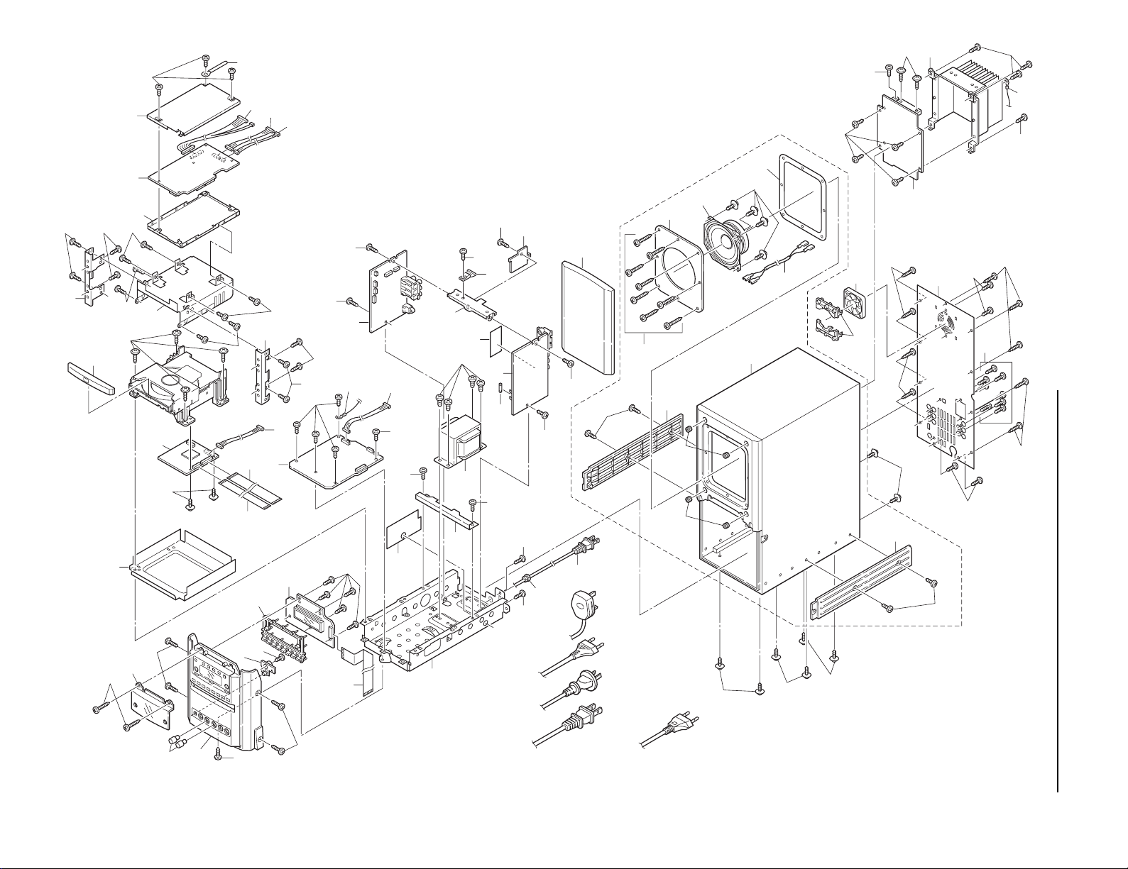
EXPLODED VIEW (CABINET & CHASSIS)
13
12
4
14
7
5
22
21
6
18
Y27
Y27
64
61
63
57
59
2
1-1
11
10
1-2
1-3
1-4
1-6
1-7
1-11
62
60
19
8
9
3
4
4
17
78
56
53
55
79
75
52
51
58
54
76
71
16
74
77
72
73
Y06
Y17 Y01
Y07
Y07
Y23
Y08
Y23
Y28
Y04
Y20
Y21
Y01
Y21
Y02
Y10
Y10
Y13
Y09
Y15
Y14
Y25
Y16
Y15
Y14
1-8
1-8
Y19
Y22
Y05
Y05
Y05
Y05
Y11
Y22
Y18
Y18
Y18
1-9
1-5
1-5
Y25
Y26
Y24
Y03
61
Y03
1-10
Y13
Y01
20
(AU)
(UK)
(US,CA)
(XE)
(KR)
Y17
- 47 -

PARTS LIST
PRODUCT SAFETY NOTICE
EACH PRECAUTION IN THIS MANUAL SHOULD BE FOLLOWED DURING SERVICING. COMPONENTS IDENTIFIED WITH THE IEC
!!
!
SYMBOL
SPECIAL SIGNIFICANCE. WHEN REPLACING A COMPONENT IDENTIFIED BY
OR PARTS WITH THE SAME RATINGS OF RESISTANCE, WATTAGE OR VOLTAGE THAT ARE DESIGNATED IN THE PARTS LIST
IN THIS MANUAL. LEAKAGE-CURRENT OR RESISTANCE MEASUREMENTS MUST BE MADE TO DETERMINE THAT EXPOSED
PARTS ARE ACCEPTABLY INSULATED FROM THE SUPPLY CIRCUIT BEFORE RETURNING THE PRODUCT TO THE CUSTOMER.
CAUTION : Regular type resistors and capacitors are not listed. To know those values, refer to the schematic diagram.
IN THE PARTS LIST AND THE SCHEMATIC DIAGRAM DESIGNATED COMPONENTS IN WHICH SAFETY CAN BE OF
!!
!
, USE ONLY THE REPLACEMENT PARTS DESIGNATED,
Regular type resistors are less than 1/4 W Carbon type and Chip type resistors.
Regular type capacitors are less than 50 V and less than 1000 µF type of Ceramic type, Electrical type and Chip type.
PACKING & ACCESSORIES
REF.NO. PART NO. DESCRIPTION
614 315 8875 CARTON CASE(1000)
614 317 9689 CARTON CASE(XE)
614 317 9696 CARTON CASE(UK)
614 318 0760 CARTON CASE(SS)
614 318 6366 CARTON CASE(KR)
614 317 3328 CARTON CASE(US)
614 318 3853 CARTON CASE(CA)
614 318 6373 CARTON CASE(AU)
614 278 9117 NOTICE(1000,US)
614 303 7484 LABEL,CAUTION,CUSHION TOP(1000)
614 315 9001 INSTRUCTION,MANUAL(1000)
614 317 9795 INSTRUCTION MANUAL(XE)
614 317 9818 INSTRUCTION MANUAL(UK)
614 318 0845 INSTRUCTION MANUAL(SS)
614 318 6434 INSTRUCTION MANUAL(KR)
614 317 3359 INSTRUCTION MANUAL(US)
614 318 3907 INSTRUCTION MANUAL(CA)
614 318 6441 INSTRUCTION MANUAL(AU)
614 317 9801 INSTRUCTION MANUAL,(GREEK)(XE)
614 317 3182 INSTRUCTION SHEET,QUICK GUIDE
(1000)
614 317 3366 INSTRUCTION,SHEET,QUICK GUIDE
(US)
614 315 8974 CUSHION,TOP
614 315 8981 CUSHION,BOTTOM
645 046 8278 POLY SHEET-1300X0500*NC,SET
(1000,UK,SS,KR,US,CA,AU)
645 047 3418 POLY SHEET-1300X0500*NC,SET(XE)
645 044 9413 REMOCON,RB-H520MT(1000,CA)
645 044 9420 REMOCON,RB-H5201ST(XE,UK,AU)
645 044 9437 REMOCON,RB-H5201(SS,KR)
645 046 8391 REMOCON,REM-H5201(US)
645 043 9735 BATTERY COVER,SERVICE PART
645 041 1373 CABLE,VIDEO,VIDEO-CABLE(1.5M)
645 047 0356 WIRE,MAIN SP
645 047 0363 WIRE,SUB WOOFER
645 017 2175 PLUG,ADAPTOR AC(SS)
or 645 006 4630 PLUG,ADAPTOR AC(SS)
CABINET & CHASSIS
REF.NO. PART NO. DESCRIPTION
1 614 315 8516 ASSY,CABINET(1000,UK,SS,KR,AU)
1 614 317 9481 ASSY,CABINET(XE)
1 614 317 3236 ASSY,CABINET(US,CA)
1-1 614 319 0523 ASSY.BOX,SPEAKER
1-2 645 048 4957 LEFT SIDE COVER
1-3 645 048 4964 RIGHT SIDE COVER
1-4 645 048 4988 MID RANGE HOLDER
1-5 645 048 4971 RUBBER CATCHER
1-6 645 048 5015 MID RANGE
1-7 645 048 5084 JOIN WIRE
1-8 645 048 5138 SCREW,SIDE COVER
1-9 645 048 5121 SCREW,MID RANGE HOLDER
1-10 645 048 5091 SCREW,MID RANGE UNIT
REF.NO. PART NO. DESCRIPTION
1-11 645 048 5169 CUSHION,MID RANGE
2 614 315 8127 ASSY,GRILLE(1000,XE,UK,SS,KR,AU)
2 614 317 3250 ASSY,GRILLE(US)
2 614 318 3648 ASSY,GRILLE(CA)
3 614 315 6611 BUTTON(1000,XE,UK,SS,KR,AU)
3 614 317 3274 BUTTON(US,CA)
4 614 315 6727 MOUNTING,PANEL
5 614 315 8134 ASSY,PANEL,FRONT(1000,XE,UK,AU)
5 614 318 0708 ASSY,PANEL,FRONT(SS,KR)
5 614 317 3267 ASSY,PANEL,FRONT(US,CA)
6 614 315 6642 CHASSIS,MECHA/TRANS/PWB
7 614 315 6666 DEC,WINDOW,FL
8 614 315 7762 HOLDER,TRANS
9 614 315 6734 MOUNTING,PWB,JACK PWB FIX
10 614 310 3837 MOUNTING,FAN
11 614 315 6765 PANEL,REAR(1000)
11 614 317 5445 PANEL,REAR(XE)
11 614 317 5452 PANEL,REAR(UK)
11 614 317 5469 PANEL,REAR(SS)
11 614 318 6182 PANEL,REAR(KR)
11 614 317 3298 PANEL,REAR(US)
11 614 318 3679 PANEL,REAR(CA)
11 614 318 6199 PANEL.REAR(AU)
12 614 314 7107 SHIELD,MPEG PWB BOTTOM
13 614 314 7114 SHIELD,MPEG PWB TOP
14 614 315 6796 SHIELD,DVD MECHA,BOTTOM
15 614 315 6802 SHIELD,DVD MECHA,TOP
16 614 307 2638 LABEL,INDICATION,FUSE(1000)
17 614 315 8110 ASSY,DEC ESCUTCHEON
(1000,XE,UK,SS,KR,AU)
17 614 317 3243 ASSY,DEC,ESCUTCHEON(US,CA)
18 614 129 1901 FIXER,AC CORD
or 614 284 1884 FIXER,AC CORD
19 614 318 0166 SPACER,SHEET,CHASSIS
(1000,US,CA)
19 614 317 2994 SPACER,SHEET,CHASSIS
(XE,UK,SS,KR,AU)
20 614 129 9136 LUG,LEAD FIX
21 614 315 6628 BUTTON,SELECT(SS,KR)
22 614 317 5438 KNOB,ROTARY,MIC/ECHO VOL(SS,KR)
614 317 3090 LABEL,SAFETY(XE,UK,AU)
FIXING PARTS
REF.NO. PART NO. DESCRIPTION
Y01 411 021 3503 SCR S-TPG BIN 3X10,
MOUNTING,PANEL
Y02 411 021 3503 SCR S-TPG BIN 3X10,FRONT PWB
Y03 645 046 8209 SCREW,HEAT SINK UNIT
Y04 645 046 8216 SCREW,PANEL FRONT SIDE
Y05 645 046 8261 SCREW,PANEL REAR
Y06 411 021 6405 SCR S-TPG BIN 3X8,
MPEG PWB-SHIELD MPEG
Y07 411 021 3503 SCR S-TPG BIN 3X10,MPEG UNIT
Y08 411 020 8905 SCR S-TPG BRZ+FLG 3X10,
DVD MECHA
- 48 -

PARTS LIST
REF.NO. PART NO. DESCRIPTION
Y09 411 001 4209 SCR S-TPG BIN 4X8,TRANS
Y10 411 021 3503 SCR S-TPG BIN 3X10,HOLDER TRANS
Y11 411 021 3701 SCR S-TPG BIN 3X10,MOUNTING FAN
Y12 411 021 3503 SCR S-TPG BIN 3X10,FRONT PWB
Y13 411 021 3503 SCR S-TPG BIN 3X10,
Y14 411 021 3503 SCR S-TPG BIN 3X10,JACK PWB L/R
Y15 411 021 3503 SCR S-TPG BIN 3X10,MOUNTING PWB
Y16 411 021 3503 SCR S-TPG BIN 3X10,JACK PWB C
Y17 411 021 3503 SCR S-TPG BIN 3X10,
Y18 411 020 8905 SCR S-TPG BRZ+FLG 3X10,
Y19 411 020 8905 SCR S-TPG BRZ+FLG 3X10,
Y20 411 021 3503 SCR S-TPG BIN 3X10,
Y21 411 123 9106 SCR S-TPG BIN 3X20,
Y22 411 021 3701 SCR S-TPG BIN 3X10,
Y23 411 021 6405 SCR S-TPG BIN 3X8,
Y24 411 021 4500 SCR S-TPG BIN 3X16,POWER IC 1
or 411 021 4500 SCR S-TPG BIN 3X16,POWER IC 2
Y25 411 021 3503 SCR S-TPG BIN 3X10,POSISTOR
or 411 021 3503 SCR S-TPG BIN 3X10,HEAT SINK 1
or 411 021 3503 SCR S-TPG BIN 3X10,HEAT SINK 2
or 411 021 3503 SCR S-TPG BIN 3X10,HEAT SINK 3
or 411 021 3503 SCR S-TPG BIN 3X10,HEAT SINK 4
Y26 411 021 6405 SCR S-TPG BIN 3X8,Q4990
Y27 411 021 1806 SCR S-TPG BIN 2.6X10,
ELECTRICAL PART
REF.NO. PART NO. DESCRIPTION
51 645 044 9567 FLEXIBLE FLAT CABLE (CN001)
52 645 044 9574 FLEXIBLE FLAT CABLE (CN002)
53 614 315 8653 ASSY,WIRE,POWER-MPEG (CN400)
54 614 315 8660 ASSY,WIRE,POWER-LODER (CN401)
55 614 315 8677 ASSY,WIRE,DIGITAL-MPEG (CN402)
56 614 315 8707 ASSY,WIRE,PRE-MPEG (CN404)
57 614 315 8745 ASSY,WIRE,PRE-POWER (CN406)
58 645 046 8421 FLEXIBLE FLAT CABLE,FRONT-PRE
59
59
or
60
61 614 129 9082 LUG,POWER PWB-GND
62 645 045 6930 MOTOR,FAN DC 0.72W(Except CA)
63
63
63
63
64
or
64
or
64
or
64
64
or
!!
!
423 028 7002 FUSE 250V 2.5A(1000,US,CA)
!!
!
423 028 8306 FUSE250V 1.25A(XE,UK,AU)
!!
!
423 005 6509 FUSE 250V 1.25A(XE,UK,AU)
!!
!
614 315 6994 ASSY,HEAT SINK,ASSY,HEAT SINK
!!
!
645 044 9635 TRANS,POWER(1000,US,CA)
!!
!
645 044 9642 TRANS,POWER(XE,UK,AU)
!!
!
645 044 9659 TRANS,POWER(SS)
!!
!
645 047 7959 TRANS,POWER(KR)
!!
!
645 037 7747 CORD,POWER-1.845MK(1000,US,CA)
!!
!
645 032 7537 CORD,POWER-1.86MK
!!
!
645 016 9939 CORD,POWER-1.74MK(XE,SS)
!!
!
614 255 2513 POWER CORD
!!
!
645 036 9797 CORD,POWER-1.6MK(UK)
!!
!
645 036 9803 POWER CORD
!!
!
645 039 2528 CORD,POWER-1.75MK(KR)
!!
!
645 032 1887 CORD,POWER-2.0MK(AU)
!!
!
614 256 5308 POWER CORD
!!
!
614 086 2164 COVER,CAPACITOR(C4300)(XE,UK)
FRONTJACK(PRE AMP) PWB
FRONT ASSY-CHASSIS ASSY
CHASSIS(BOTTOM SIDE)
CHASSIS(BACK SIDE)
PANEL FRONT(BOTTOM SIDE)
PANEL FRONT(L/R SIDE)
PANEL REAR/ELECT PARTS
SHIELD MECHA TOP
VOLTAGE SELECTOR(SS)
MPEG-LOADER 16P
MPEG-LOADER 26P
SOCKET-A P.W.BOARD ASSY
REF.NO. PART NO. DESCRIPTION
71 614 314 5721 ASSY,PWB,SOCKET-A(Only initial)
(1000,US,CA)
71 614 318 0234 ASSY,PWB,SOCKET-A(Only initial)(SS)
71 614 318 5529 ASSY,PWB,SOCKET-A(Only initial)(KR)
71 614 318 5826 ASSY,PWB,SOCKET-A(Only initial)(AU)
CN429 614 315 8776 ASSY,WIRE,POWER-AUDIO
(SS,KR,AU)
CN430 614 315 8776 ASSY,WIRE,POWER-AUDIO
(1000,US,CA)
CN430 645 005 9315 PLUG,2P(SS)
CN431 645 005 9315 PLUG,2P(1000,KR,US,CA,AU)
CN431 645 030 9878 PLUG,3P(SS)
CN432 645 045 7500 JACK,RCA-4
CN433 645 038 3670 JACK,RCA
CN434 645 011 8210 TERMINAL
CN435 645 023 4378 SOCKET,7P
CN436 614 315 8714 ASSY,WIRE,SOCKET_A-PRE
CN437 614 315 8691 ASSY,WIRE,VIDEO-SOCKET_A
CN438 614 310 2434 PLUG,2P
or 645 005 7366 PLUG,2P
CN439 614 310 2298 PLUG,2P
or 645 004 2683 PLUG,2P
CN491 645 031 7903 HOLDER,FUSE
or 645 006 4760 HOLDER,FUSE
CN492 645 031 7903 HOLDER,FUSE
or 645 006 4760 HOLDER,FUSE
CN493 645 031 7903 HOLDER,FUSE(SS)
or 645 006 4760 HOLDER,FUSE
CN494 645 031 7903 HOLDER,FUSE(SS)
or 645 006 4760 HOLDER,FUSE
!!
L4300
!
645 038 7364 INDUCTOR,70U
LUG43 645 023 8987 FIXER
!!
R4300
or
or
R4371
!
402 080 9803 CARBON 3.3M J- 1/2W
!!
!
402 078 8108 CARBON 3.3M J- 1/2W
!!
!
402 078 9501 CARBON 3.3M J- 1/2W
!!
!
614 241 3449 RESISTOR 0.22 K- 5W
S4399 645 031 5800 SWITCH,SLIDE 2P-2T(SS)
WR430 614 017 6964 TERMINAL BOARD
WR431 614 017 6964 TERMINAL BOARD
SOCKET-A P.W.BOARD ASSY
REF.NO. PART NO. DESCRIPTION
71 614 317 9351 ASSY,PWB,SOCKET-A,ASSY
!!
C4300
or
!
403 349 3303 CERAMIC 0.01U M 250V
!!
!
403 366 7803 CERAMIC 0.01U M 250V
C4305 403 329 5501 ELECT 2200U M 16V
C4311 404 079 6107 ELECT 47U M 16V
CN429 614 315 8776 ASSY,WIRE,POWER-AUDIO
CN430 645 005 9315 PLUG,2P
CN431 614 315 8684 ASSY,WIRE,VIDEO-SOCKET_A
CN432 645 045 7500 JACK,RCA-4
CN433 645 038 3670 JACK,RCA
CN434 645 011 8210 TERMINAL
CN435 645 023 4378 SOCKET,7P
CN436 614 315 8714 ASSY,WIRE,SOCKET_A-PRE
CN437 614 315 8691 ASSY,WIRE,VIDEO-SOCKET_A
CN438 614 310 2434 PLUG,2P
or 645 005 7366 PLUG,2P
CN439 614 310 2298 PLUG,2P
or 645 004 2683 PLUG,2P
CN491 645 031 7903 HOLDER,FUSE
or 645 006 4760 HOLDER,FUSE
CN492 645 031 7903 HOLDER,FUSE
or 645 006 4760 HOLDER,FUSE
!!
D4301
D4302
D4303
!
407 097 8009 DIODE MPG06G
!!
!
407 097 8009 DIODE MPG06G
!!
!
407 097 8009 DIODE MPG06G
(Only initial)(XE,UK)
- 49 -

PARTS LIST
REF.NO. PART NO. DESCRIPTION REF.NO. PART NO. DESCRIPTION
D4304
D4312 407 099 5402 ZENER DIODE MTZJ6.2B
D4313 407 012 4406 DIODE 1SS133
L4300
LUG43 645 023 8987 FIXER
Q4310 405 141 3208 TR KTC3198-Y
or 405 141 3307 TR KTC3198-GR
or 405 019 2708 TR 2SC536-F-NP
or 405 019 3804 TR 2SC536-G-NP
Q4311 405 141 3208 TR KTC3198-Y
or 405 141 3307 TR KTC3198-GR
or 405 019 2708 TR 2SC536-F-NP
or 405 019 3804 TR 2SC536-G-NP
R4371
RY430
or
T4300
WR430 614 017 8203 TERMINAL BOARD
WR431 614 017 8203 TERMINAL BOARD
DIGITAL OUT P.W.BOARD ASSY
REF.NO. PART NO. DESCRIPTION
72 614 314 5738 ASSY,PWB,SW(Only initial)
72 614 317 9368 ASSY,PWB,SW(Only initial)(XE,UK)
72 614 318 0241 ASSY,PWB,SW(Only initial)(SS)
72 614 318 5536 ASSY,PWB,SW(Only initial)(KR)
72 614 318 7417 ASSY,PWB,SW(Only initial)(AU)
CN420 407 218 1100 PHOTO COUPLE GP1FA550TZ
or 407 215 1608 PHOTO COUPLE TOTX178A
CN421 614 310 2458 PLUG,4P
or 645 005 8110 PLUG,4P
S4200 645 040 6119 SWITCH,SLIDE 2P-2TX2,
FRONT P.W.BOARD ASSY
REF.NO. PART NO. DESCRIPTION
73 614 314 5776 ASSY,PWB,FRONT(Only initial)
73 614 317 9375 ASSY,PWB,FRONT(Only initial)(XE,UK)
73 614 318 0258 ASSY,PWB,FRONT(Only initial)(SS,KR)
73 614 318 5833 ASSY,PWB,FRONT(Only initial)(AU)
BR601 614 315 5843 HOLDER,FL,FL_MOUNT
CN601 645 012 5515 SOCKET,FPC 18P
CN602 614 315 8530 ASSY,WIRE
CN603 614 315 8530 ASSY,WIRE
D6001 407 012 4406 DIODE 1SS133
D6002 407 012 4406 DIODE 1SS133
D6003 407 012 4406 DIODE 1SS133
D6004 407 003 4507 DIODE DAP202K
D6850 408 044 8509 LED SLZ-9G55B-24HAB-T1
D6851 408 044 8509 LED SLZ-9G55B-24HAB-T1
D6852 408 044 8509 LED SLZ-9G55B-24HAB-T1
D6853 408 044 8509 LED SLZ-9G55B-24HAB-T1
D6870 407 115 1302 LED SLP-144B-51-A,STANDBY
DS601 407 217 1101 PHOTO DIODE SPS-442-1G,IR
FL601 645 044 8232 FLUORESCENT TUBE,FL
IC601 410 404 1006 IC LC866540A-5V28,MICON
L6000 645 001 4550 INDUCTOR,10U K
or 645 031 7835 INDUCTOR,10U K
Q6001 405 146 2107 TR KTC3875-Y
or 405 146 2206 TR KTC3875-GR
or 405 014 4509 TR 2SC2412K-R
or 405 011 1006 TR 2SC1623-L6
Q6004 405 146 5306 TR KRA102S(SS)
or 405 000 0409 TR DTA114EK
Q6006 405 146 2107 TR KTC3875-Y(SS)
or 405 146 2206 TR KTC3875-GR
or 405 014 4509 TR 2SC2412K-R
or 405 011 1006 TR 2SC1623-L6
!!
!
407 097 8009 DIODE MPG06G
!!
!
645 038 7364 INDUCTOR,70U
!!
!
614 241 3449 RESISTOR 0.22 K- 5W
!!
!
645 030 5597 RELAY,PRIMARY
!!
!
645 035 6575 RELAY,PRIMARY
!!
!
645 041 4954 TRANS,POWER
PAL-NTSC(XE,UK,AU)
(1000,US,CA)
(1000,US,CA)
S6100 645 006 5958 SWITCH,PUSH 1P-1T
S6101 645 006 5958 SWITCH,PUSH 1P-1T
S6102 645 006 5958 SWITCH,PUSH 1P-1T
S6103 645 006 5958 SWITCH,PUSH 1P-1T
S6115 645 006 5958 SWITCH,PUSH 1P-1T
S6116 645 006 5958 SWITCH,PUSH 1P-1T
S6117 645 006 5958 SWITCH,PUSH 1P-1T
S6118 645 006 5958 SWITCH,PUSH 1P-1T
S6119 645 006 5958 SWITCH,PUSH 1P-1T
S6120 645 006 5958 SWITCH,PUSH 1P-1T
X6002 645 018 6103 OSC,CERAMIC 6.000MHZ
POWER AMP P.W.BOARD ASSY
REF.NO. PART NO. DESCRIPTION
74 614 314 5783 ASSY,PWB,POWER(Only initial)
74 614 317 9382 ASSY,PWB,POWER(Only initial)(XE,UK)
74 614 318 0265 ASSY,PWB,POWER(Only initial)(SS,KR)
74 614 318 5840 ASSY,PWB,POWER(Only initial)(AU)
C4705 403 057 2407 POLYESTER 0.1U J 50V
C4706 403 057 2407 POLYESTER 0.1U J 50V
C4750 403 185 0108 MT-POLYEST 0.47U J 50V
C4751 403 184 9805 MT-POLYEST 0.22U J 50V
C4805 403 057 2407 POLYESTER 0.1U J 50V
C4806 403 057 2407 POLYESTER 0.1U J 50V
C4825 403 057 2407 POLYESTER 0.1U J 50V
C4826 403 057 2407 POLYESTER 0.1U J 50V
C4900 403 329 6201 ELECT 2200U M 35V
!!
C4900
!
404 085 9505 ELECT 2200U M 35V(XE,UK)
C4901 403 329 6201 ELECT 2200U M 35V
!!
C4901
!
404 085 9505 ELECT 2200U M 35V(XE,UK)
C4910 403 329 6201 ELECT 2200U M 35V
!!
C4910
!
404 085 9505 ELECT 2200U M 35V(XE,UK)
C4914 403 326 2503 ELECT 1200U M 10V
C4918 404 079 6305 ELECT 10U M 50V(1000,US,CA)
C4924 403 337 1205 ELECT 1200U M 6.3V
CN470 614 310 2496 PLUG,8P
or 645 005 8134 PLUG,8P
CN471 614 310 2342 PLUG,7P
or 645 004 2737 PLUG,7P
CN472 614 310 2465 PLUG,5P
or 645 005 9292 PLUG,5P
CN473 614 315 8752 ASSY,WIRE,POWER-SOCKET_A
CN474 614 310 2458 PLUG,4P
or 645 005 8110 PLUG,4P
CN475 645 006 0939 PLUG,6P
or 614 310 2625 PLUG,6P
CN476 645 006 0960 PLUG,9P
or 614 310 2656 PLUG,9P
CN477 645 006 1905 PLUG,5P
D4730 407 012 4406 DIODE 1SS133
D4731 407 012 4406 DIODE 1SS133
D4750 407 012 4406 DIODE 1SS133
!!
D4900
D4904
D4905
D4906
D4907
!
408 043 8005 DIODE G5SBA60L-BU04
!!
!
407 196 5800 DIODE 1N5402BD82
!!
!
407 196 5800 DIODE 1N5402BD82
!!
!
408 044 6208 DIODE SB240L 19C2-105
!!
!
408 044 6208 DIODE SB240L 19C2-105
HS490 614 264 0159 HEAT SINK(XE,UK,SS,KR)
!!
IC470
IC491
IC492
or
IC493
!
409 473 9501 IC STK402-230
!!
!
409 499 5808 IC PQ1CZ31H2ZP,PQ1CZ31H2ZP
!!
!
409 463 6701 IC KIA7805API
!!
!
409 145 2809 IC NJM7805FA
!!
!
409 499 5808 IC PQ1CZ31H2ZP,PQ1CZ31H2ZP
L4700 614 202 1712 V.H.F COIL 1AV4L20B0320N
or 614 196 9763 V.H.F COIL
(1000,SS,KR,US,CA,AU)
(1000,SS,KR,US,CA,AU)
(1000,SS,KR,US,CA,AU)
(1000,US,CA)
- 50 -

PARTS LIST
L4800 614 202 1712 V.H.F COIL 1AV4L20B0320N
or 614 196 9763 V.H.F COIL
L4820 614 202 1712 V.H.F COIL 1AV4L20B0320N
or 614 196 9763 V.H.F COIL
L4900 645 043 3054 INDUCTOR,10U
L4901
L4902 645 043 3054 INDUCTOR,10U
L4904
L4905 645 043 3054 INDUCTOR,10U
PR490
PR491
PR492
PR493
Q4700 405 143 8706 TR KTC3199-GR
or 405 017 9600 TR 2SC3330-T
or 405 017 9709 TR 2SC3330-U
or 405 011 8500 TR 2SC1740S-R
or 405 011 8609 TR 2SC1740S-S
Q4730 405 143 8706 TR KTC3199-GR
or 405 017 9600 TR 2SC3330-T
or 405 017 9709 TR 2SC3330-U
or 405 011 8500 TR 2SC1740S-R
or 405 011 8609 TR 2SC1740S-S
Q4731 405 143 6504 TR KTA1267-GR
or 405 004 4601 TR 2SA608-F-SPA
or 405 004 5103 TR 2SA608-G-SPA
or 405 006 1806 TR 2SA933S-R
or 405 006 1905 TR 2SA933S-S
Q4732 405 143 8706 TR KTC3199-GR
or 405 017 9600 TR 2SC3330-T
or 405 017 9709 TR 2SC3330-U
or 405 011 8500 TR 2SC1740S-R
or 405 011 8609 TR 2SC1740S-S
Q4733 405 143 8706 TR KTC3199-GR
or 405 017 9600 TR 2SC3330-T
or 405 017 9709 TR 2SC3330-U
or 405 011 8500 TR 2SC1740S-R
or 405 011 8609 TR 2SC1740S-S
Q4734 405 143 8706 TR KTC3199-GR
or 405 017 9600 TR 2SC3330-T
or 405 017 9709 TR 2SC3330-U
or 405 011 8500 TR 2SC1740S-R
or 405 011 8609 TR 2SC1740S-S
Q4735 405 143 8706 TR KTC3199-GR
or 405 017 9600 TR 2SC3330-T
or 405 017 9709 TR 2SC3330-U
or 405 011 8500 TR 2SC1740S-R
or 405 011 8609 TR 2SC1740S-S
Q4736 405 143 8706 TR KTC3199-GR
or 405 017 9600 TR 2SC3330-T
or 405 017 9709 TR 2SC3330-U
or 405 011 8500 TR 2SC1740S-R
or 405 011 8609 TR 2SC1740S-S
Q4737 405 143 8706 TR KTC3199-GR
or 405 017 9600 TR 2SC3330-T
or 405 017 9709 TR 2SC3330-U
or 405 011 8500 TR 2SC1740S-R
or 405 011 8609 TR 2SC1740S-S
Q4738 405 141 3208 TR KTC3198-Y
or 405 141 3307 TR KTC3198-GR
or 405 019 2708 TR 2SC536-F-NP
or 405 019 3804 TR 2SC536-G-NP
Q4739 405 143 8706 TR KTC3199-GR
or 405 017 9600 TR 2SC3330-T
or 405 017 9709 TR 2SC3330-U
or 405 011 8500 TR 2SC1740S-R
or 405 011 8609 TR 2SC1740S-S
Q4740 405 143 8706 TR KTC3199-GR
or 405 017 9600 TR 2SC3330-T
or 405 017 9709 TR 2SC3330-U
!!
!
645 045 7241 INDUCTOR,65U
!!
!
645 045 7241 INDUCTOR,65U
!!
!
645 042 2720 PROTECTOR,5A 125V
!!
!
645 042 2652 PROTECTOR,10A 125V
!!
!
645 042 2720 PROTECTOR,5A 125V
!!
!
645 042 2652 PROTECTOR,10A 125V
REF.NO. PART NO. DESCRIPTIONREF.NO. PART NO. DESCRIPTION
or 405 011 8500 TR 2SC1740S-R
or 405 011 8609 TR 2SC1740S-S
Q4741 405 143 8706 TR KTC3199-GR
or 405 017 9600 TR 2SC3330-T
or 405 017 9709 TR 2SC3330-U
or 405 011 8500 TR 2SC1740S-R
or 405 011 8609 TR 2SC1740S-S
Q4750 405 143 8706 TR KTC3199-GR
or 405 017 9600 TR 2SC3330-T
or 405 017 9709 TR 2SC3330-U
or 405 011 8500 TR 2SC1740S-R
or 405 011 8609 TR 2SC1740S-S
Q4800 405 143 8706 TR KTC3199-GR
or 405 017 9600 TR 2SC3330-T
or 405 017 9709 TR 2SC3330-U
or 405 011 8500 TR 2SC1740S-R
or 405 011 8609 TR 2SC1740S-S
Q4820 405 143 8706 TR KTC3199-GR
or 405 017 9600 TR 2SC3330-T
or 405 017 9709 TR 2SC3330-U
or 405 011 8500 TR 2SC1740S-R
or 405 011 8609 TR 2SC1740S-S
Q4910 405 146 1605 TR KRC102S
or 405 000 2908 TR DTC114EK
Q4911 405 146 1605 TR KRC102S
or 405 000 2908 TR DTC114EK
Q4912 405 146 1605 TR KRC102S
or 405 000 2908 TR DTC114EK
Q4920 405 143 8706 TR KTC3199-GR
or 405 017 9600 TR 2SC3330-T
or 405 017 9709 TR 2SC3330-U
or 405 011 8500 TR 2SC1740S-R
or 405 011 8609 TR 2SC1740S-S
!!
R4706
R4707
R4708
R4716
R4717
R4730
!
402 081 0403 RESISTOR 4.7 J- 2W
!!
!
402 081 0502 RESISTOR 330 J- 3W
!!
!
402 081 0403 RESISTOR 4.7 J- 2W
!!
!
402 081 1103 FUSIBLE RES 100 JA 1/4W
!!
!
402 081 1103 FUSIBLE RES 100 JA 1/4W
!!
!
614 241 3449 RESISTOR 0.22 K- 5W
R4799 408 017 0806 TH PTH9M04BB471TS2F333
!!
R4806
R4807
R4808
R4826
R4828
!
402 081 0403 RESISTOR 4.7 J- 2W
!!
!
402 081 0502 RESISTOR 330 J- 3W
!!
!
402 081 0403 RESISTOR 4.7 J- 2W
!!
!
402 081 0403 RESISTOR 4.7 J- 2W
!!
!
402 081 0403 RESISTOR 4.7 J- 2W
RY470 614 224 4531 RELAY,SPEAKER
or 645 035 6582 RELAY,SPEAKER
RY480 645 046 1279 RELAY,SPEAKER
or 645 046 1743 RELAY,SPEAKER
PRE AMPLIFIER P.W.BOARD ASSY
REF.NO. PART NO. DESCRIPTION
75 614 315 8080 ASSY,PWB,PRE(Only initial)
75 614 317 9399 ASSY,PWB,PRE(Only initial)(XE,UK)
75 614 318 0272 ASSY,PWB,PRE(Only initial)(SS,KR)
75 614 318 5857 ASSY,PWB,PRE(Only initial)(AU)
CN440 614 315 8738 ASSY,WIRE,POWER-PRE
CN441 645 047 2060 JACK,PHONE D3.6
CN442 645 047 2060 JACK,PHONE D3.6
CN443 645 047 2060 JACK,PHONE D3.6 (SS,KR)
CN445 614 035 4942 SOCKET,DIP 5P
CN451 614 310 2472 PLUG,6P
or 645 005 8127 PLUG,6P
CN452 614 310 2441 PLUG,3P
or 645 005 7373 PLUG,3P
CN453 645 012 5515 SOCKET,FPC 18P
CN456 614 310 2496 PLUG,8P
or 645 005 8134 PLUG,8P
(1000,US,CA)
- 51 -

PARTS LIST
REF.NO. PART NO. DESCRIPTION REF.NO. PART NO. DESCRIPTION
CN457 614 315 8530 ASSY,WIRE,VIDEO-PRE
D4560 407 099 5303 ZENER DIODE MTZJ5.6B(SS,KR)
D4561 407 012 4406 DIODE 1SS133(SS,KR)
D4562 407 012 4406 DIODE 1SS133(SS,KR)
IC450 409 474 6103 IC LC75342M
IC451 409 478 1104 IC LA2615M,SURROUND
IC452 409 426 1804 IC KIA4558S
IC453 409 426 1804 IC KIA4558S
IC455 409 390 8908 IC BA3838F(SS,KR)
IC456 409 294 6109 IC TA2011S(SS,KR)
IC457 409 400 9505 IC BU9255FS(SS,KR)
L4401 645 001 4581 INDUCTOR,100U K(Eecept XE,UK)
or 645 031 7842 INDUCTOR,100U K
L4401 645 006 9864 INDUCTOR,80U(XE,UK)
or 645 212 3171 INDUCTOR,FERITE
L4402 645 001 4581 INDUCTOR,100U K(Eecept XE,UK)
or 645 031 7842 INDUCTOR,100U K
L4402 645 006 9864 INDUCTOR,80U(XE,UK)
or 645 212 3171 INDUCTOR,FERITE
L4403 645 001 4581 INDUCTOR,100U K(Eecept XE,UK)
or 645 031 7842 INDUCTOR,100U K
L4404 645 001 4581 INDUCTOR,100U K(Eecept XE,UK)
or 645 031 7842 INDUCTOR,100U K
L4451 645 001 4581 INDUCTOR,100U K(Eecept XE,UK)
or 645 031 7842 INDUCTOR,100U K
L4451 645 006 9864 INDUCTOR,80U(XE,UK)
or 645 212 3171 INDUCTOR,FERITE
L4452 645 001 4581 INDUCTOR,100U K(Eecept XE,UK)
or 645 031 7842 INDUCTOR,100U K
L4452 645 006 9864 INDUCTOR,80U(XE,UK)
or 645 212 3171 INDUCTOR,FERITE
L4453 645 001 4581 INDUCTOR,100U K(Eecept XE,UK)
or 645 031 7842 INDUCTOR,100U K
L4454 645 001 4581 INDUCTOR,100U K(Eecept XE,UK)
or 645 031 7842 INDUCTOR,100U K
Q4430 405 151 4400 TR KTD1303
or 405 021 0204 TR 2SD1012-F-SPA
or 405 021 0600 TR 2SD1012-G-SPA
or 405 033 6706 TR 2SD1468S-R
or 405 033 6805 TR 2SD1468S-S
Q4480 405 151 4400 TR KTD1303
or 405 021 0204 TR 2SD1012-F-SPA
or 405 021 0600 TR 2SD1012-G-SPA
or 405 033 6706 TR 2SD1468S-R
or 405 033 6805 TR 2SD1468S-S
Q4500 405 151 4400 TR KTD1303
or 405 021 0204 TR 2SD1012-F-SPA
or 405 021 0600 TR 2SD1012-G-SPA
or 405 033 6706 TR 2SD1468S-R
or 405 033 6805 TR 2SD1468S-S
Q4520 405 151 4400 TR KTD1303(SS,KR)
or 405 021 0204 TR 2SD1012-F-SPA
or 405 021 0600 TR 2SD1012-G-SPA
or 405 033 6706 TR 2SD1468S-R
or 405 033 6805 TR 2SD1468S-S
Q4531 405 143 6504 TR KTA1267-GR
or 405 004 4601 TR 2SA608-F-SPA
or 405 004 5103 TR 2SA608-G-SPA
or 405 006 1806 TR 2SA933S-R
or 405 006 1905 TR 2SA933S-S
Q4532 405 143 8706 TR KTC3199-GR
or 405 017 9600 TR 2SC3330-T
or 405 017 9709 TR 2SC3330-U
or 405 011 8500 TR 2SC1740S-R
or 405 011 8609 TR 2SC1740S-S
Q4535 405 143 6504 TR KTA1267-GR
or 405 004 4601 TR 2SA608-F-SPA
or 405 004 5103 TR 2SA608-G-SPA
or 405 006 1806 TR 2SA933S-R
or 405 006 1905 TR 2SA933S-S
Q4536 405 143 8706 TR KTC3199-GR
or 405 017 9600 TR 2SC3330-T
or 405 017 9709 TR 2SC3330-U
or 405 011 8500 TR 2SC1740S-R
or 405 011 8609 TR 2SC1740S-S
Q4560 405 143 8706 TR KTC3199-GR(SS,KR)
or 405 017 9600 TR 2SC3330-T
or 405 017 9709 TR 2SC3330-U
or 405 011 8500 TR 2SC1740S-R
or 405 011 8609 TR 2SC1740S-S
Q4561 405 143 8706 TR KTC3199-GR(SS,KR)
or 405 017 9600 TR 2SC3330-T
or 405 017 9709 TR 2SC3330-U
or 405 011 8500 TR 2SC1740S-R
or 405 011 8609 TR 2SC1740S-S
Q4562 405 109 9204 TR KRC102M-A(SS,KR)
or 405 000 3103 TR DTC114ES
Q4563 405 109 9204 TR KRC102M-A(SS,KR)
or 405 000 3103 TR DTC114ES
Q4600 405 151 4400 TR KTD1303
or 405 021 0204 TR 2SD1012-F-SPA
or 405 021 0600 TR 2SD1012-G-SPA
or 405 033 6706 TR 2SD1468S-R
or 405 033 6805 TR 2SD1468S-S
S4400 614 215 9828 SWITCH,TACT,VOCALFADER
VR440 645 012 3054 VR,ROTARY 10KB
VR441 645 012 3054 VR,ROTARY 10KB
VIDEO P.W.BOARD ASSY
REF.NO. PART NO. DESCRIPTION
76 614 315 8097 ASSY,PWB,VIDEO(Only initial)
76 614 317 9405 ASSY,PWB,VIDEO(Only initial)(XE,UK)
76 614 318 0289 ASSY,PWB,VIDEO(Only initial)(SS,KR)
76 614 318 5864 ASSY,PWB,VIDEO(Only initial)(AU)
C4112 403 325 0401 ELECT 1000U M 6.3V
C4970 403 329 6201 ELECT 2200U M 35V
C4971 403 329 6102 ELECT 1000U M 35V
CN410 614 310 2526 PLUG,11P
or 645 005 8165 PLUG,11P
CN411 645 041 1298 JACK,RCA-6)(1000,SS,KR,US,CA)
CN411 645 041 1694 JACK,RCA-3(XE,UK)
CN412 645 044 9086 SOCKET,DIN 4P
CN413 614 035 4928 SOCKET,DIP 3P
CN415 645 021 1508 SOCKET,RGB 21P(XE,UK)
CN416 614 310 2434 PLUG,2P
or 645 005 7366 PLUG,2P
CN417 614 310 2496 PLUG,8P
or 645 005 8134 PLUG,8P
CN495 645 006 0922 PLUG,5P
or 614 310 2618 PLUG,5P
CN496 645 006 0953 PLUG,8P
or 614 310 2649 PLUG,8P
CN497 614 315 8783 ASSY,WIRE,VIDEO-POWER
CN498 645 005 8226 PLUG,3P(XE,UK)
or 614 310 2595 PLUG,3P
D4101 407 218 9205 ZENER DI0DE KDZ15V(XE,UK)
or 407 187 8001 ZENER DIODE UDZ10B
or 407 206 5608 ZENER DIODE UDZS10B
or 407 179 1003 ZENER DIODE UDZ15B
or 407 218 7409 ZENER DIODE UDZS15B
D4102 407 218 9205 ZENER DI0DE KDZ15V(XE,UK)
or 407 187 8001 ZENER DIODE UDZ10B
or 407 206 5608 ZENER DIODE UDZS10B
or 407 179 1003 ZENER DIODE UDZ15B
or 407 218 7409 ZENER DIODE UDZS15B
D4103 407 218 9205 ZENER DI0DE KDZ15V(XE,UK)
or 407 187 8001 ZENER DIODE UDZ10B
or 407 206 5608 ZENER DIODE UDZS10B
or 407 179 1003 ZENER DIODE UDZ15B
or 407 218 7409 ZENER DIODE UDZS15B
(1000,US,CA)
- 52 -

PARTS LIST
REF.NO. PART NO. DESCRIPTION
D4104 407 218 9205 ZENER DI0DE KDZ15V(XE,UK)
or 407 187 8001 ZENER DIODE UDZ10B
or 407 206 5608 ZENER DIODE UDZS10B
or 407 179 1003 ZENER DIODE UDZ15B
or 407 218 7409 ZENER DIODE UDZS15B
D4105 407 218 9205 ZENER DI0DE KDZ15V(XE,UK)
or 407 187 8001 ZENER DIODE UDZ10B
or 407 206 5608 ZENER DIODE UDZS10B
or 407 179 1003 ZENER DIODE UDZ15B
or 407 218 7409 ZENER DIODE UDZS15B
D4106 407 218 9205 ZENER DI0DE KDZ15V(XE,UK)
or 407 187 8001 ZENER DIODE UDZ10B
or 407 206 5608 ZENER DIODE UDZS10B
or 407 179 1003 ZENER DIODE UDZ15B
or 407 218 7409 ZENER DIODE UDZS15B
D4107 407 218 9205 ZENER DI0DE KDZ15V(XE,UK)
or 407 187 8001 ZENER DIODE UDZ10B
or 407 206 5608 ZENER DIODE UDZS10B
or 407 179 1003 ZENER DIODE UDZ15B
or 407 218 7409 ZENER DIODE UDZS15B
D4108 407 218 9205 ZENER DI0DE KDZ15V(XE,UK)
or 407 187 8001 ZENER DIODE UDZ10B
or 407 206 5608 ZENER DIODE UDZS10B
or 407 179 1003 ZENER DIODE UDZ15B
or 407 218 7409 ZENER DIODE UDZS15B
D4109 407 218 9205 ZENER DI0DE KDZ15V(XE,UK)
or 407 187 8001 ZENER DIODE UDZ10B
or 407 206 5608 ZENER DIODE UDZS10B
or 407 179 1003 ZENER DIODE UDZ15B
or 407 218 7409 ZENER DIODE UDZS15B
D4110 407 218 9205 ZENER DI0DE KDZ15V(XE,UK)
or 407 187 8001 ZENER DIODE UDZ10B
or 407 206 5608 ZENER DIODE UDZS10B
or 407 179 1003 ZENER DIODE UDZ15B
or 407 218 7409 ZENER DIODE UDZS15B
D4111 407 218 9205 ZENER DI0DE KDZ15V
or 407 187 8001 ZENER DIODE UDZ10B
or 407 206 5608 ZENER DIODE UDZS10B
or 407 179 1003 ZENER DIODE UDZ15B
or 407 218 7409 ZENER DIODE UDZS15B
D4112 407 218 9205 ZENER DI0DE KDZ15V
or 407 187 8001 ZENER DIODE UDZ10B
or 407 206 5608 ZENER DIODE UDZS10B
or 407 179 1003 ZENER DIODE UDZ15B
or 407 218 7409 ZENER DIODE UDZS15B
D4113 407 012 4406 DIODE 1SS133(XE,UK)
D4114 407 012 4406 DIODE 1SS133(XE,UK)
D4954 407 012 4406 DIODE 1SS133
D4955 407 012 4406 DIODE 1SS133
D4956 407 012 4406 DIODE 1SS133
D4957 407 012 4406 DIODE 1SS133
D4958 407 099 9509 ZENER DIODE MTZJ30B
D4959 407 099 5204 ZENER DIODE MTZJ5.1B
D4960 407 099 4603 ZENER DIODE MTZJ3.9B
D4961 407 012 4406 DIODE 1SS133
D4962 407 099 6102 ZENER DIODE MTZJ10B
D4963 407 012 4406 DIODE 1SS133
D4964
D4965
D4966 407 012 4406 DIODE 1SS133
D4970
D4971
D4972
D4973
D4974 407 099 4603 ZENER DIODE MTZJ3.9B
D4975 407 099 6805 ZENER DIODE MTZJ13B
D4976 407 099 6805 ZENER DIODE MTZJ13B
HS410 614 270 2598 HEAT SINK
IC410 409 499 5907 IC MM1508XNRE,MM1508XNRE
IC495
or
!!
!
407 097 8009 DIODE MPG06G(XE,UK)
!!
!
407 097 8009 DIODE MPG06G(XE,UK)
!!
!
407 097 8009 DIODE MPG06G
!!
!
407 097 8009 DIODE MPG06G
!!
!
407 098 3300 DIODE RL153-BF-S2
!!
!
407 098 3300 DIODE RL153-BF-S2
!!
!
409 463 6701 IC KIA7805API
!!
!
409 145 2809 IC NJM7805FA
REF.NO. PART NO. DESCRIPTION
L4100 645 034 7887 INDUCTOR,1000 OHM(XE,UK)
or 645 020 1813 INDUCTOR,1000 OHM
L4101 645 034 7887 INDUCTOR,1000 OHM(XE,UK)
or 645 020 1813 INDUCTOR,1000 OHM
LUG41 645 023 8987 FIXER
!!
PR410
or
PR411
PR495
PR496
PR497
or
PR498
!
645 042 2577 PROTECTOR,0.8A 125V(XE,UK)
!!
!
645 014 2505 PROTECTOR,0.8A 125V
!!
!
645 027 4169 PROTECTOR,0.125A 125V
!!
!
645 042 2720 PROTECTOR,5A 125V
!!
!
645 042 2720 PROTECTOR,5A 125V
!!
!
645 042 2577 PROTECTOR,0.8A 125V
!!
!
645 014 2505 PROTECTOR,0.8A 125V
!!
!
645 027 4169 PROTECTOR,0.125A 125V
Q4100 405 151 4400 TR KTD1303
or 405 021 0204 TR 2SD1012-F-SPA
or 405 021 0600 TR 2SD1012-G-SPA
or 405 033 6706 TR 2SD1468S-R
or 405 033 6805 TR 2SD1468S-S
Q4101 405 151 4400 TR KTD1303
or 405 021 0204 TR 2SD1012-F-SPA
or 405 021 0600 TR 2SD1012-G-SPA
or 405 033 6706 TR 2SD1468S-R
or 405 033 6805 TR 2SD1468S-S
Q4102 405 146 2107 TR KTC3875-Y(XE,UK)
or 405 146 2206 TR KTC3875-GR
or 405 014 4509 TR 2SC2412K-R
or 405 011 1006 TR 2SC1623-L6
Q4120 405 146 1605 TR KRC102S(XE,UK)
or 405 000 2908 TR DTC114EK
Q4121 405 146 5306 TR KRA102S(XE,UK)
or 405 000 0409 TR DTA114EK
Q4950 405 141 3703 TR KTA1271-Y
or 405 008 2405 TR 2SB698-F
or 405 008 2504 TR 2SB698-G
Q4951 405 146 1704 TR KTA1504-Y
or 405 146 9700 TR KTA1504-GR
or 405 005 5508 TR 2SA812-M6
Q4952 405 146 1704 TR KTA1504-Y
or 405 146 9700 TR KTA1504-GR
or 405 005 5508 TR 2SA812-M6
Q4970 405 143 6504 TR KTA1267-GR
or 405 004 4601 TR 2SA608-F-SPA
or 405 004 5103 TR 2SA608-G-SPA
or 405 006 1806 TR 2SA933S-R
or 405 006 1905 TR 2SA933S-S
Q4971 405 143 6504 TR KTA1267-GR
or 405 004 4601 TR 2SA608-F-SPA
or 405 004 5103 TR 2SA608-G-SPA
or 405 006 1806 TR 2SA933S-R
or 405 006 1905 TR 2SA933S-S
Q4973 405 143 8706 TR KTC3199-GR
or 405 017 9600 TR 2SC3330-T
or 405 017 9709 TR 2SC3330-U
or 405 011 8500 TR 2SC1740S-R
or 405 011 8609 TR 2SC1740S-S
Q4974 405 143 8706 TR KTC3199-GR
or 405 017 9600 TR 2SC3330-T
or 405 017 9709 TR 2SC3330-U
or 405 011 8500 TR 2SC1740S-R
or 405 011 8609 TR 2SC1740S-S
Q4975 405 143 8706 TR KTC3199-GR
or 405 017 9600 TR 2SC3330-T
or 405 017 9709 TR 2SC3330-U
or 405 011 8500 TR 2SC1740S-R
or 405 011 8609 TR 2SC1740S-S
!!
R4960
!
402 084 7201 FUSIBLE RES 18
R4970 401 105 1709 MT-GLAZE 150K JA 1/16W(XE,UK)
R4971 401 105 8104 MT-GLAZE 56K JA 1/16W(XE,UK)
!!
R4974
R4975
!
402 081 0601 RESISTOR 1K J- 2W
!!
!
402 081 8904 RESISTOR 1 J- 1/2W
S4100 645 040 6102 SWITCH,SLIDE 2P-2TX4
SH410 614 314 7176 SHIELD,SCART(XE,UK)
- 53 -

PARTS LIST
REGULATOR P.W.BOARD ASSY
REF.NO. PART NO. DESCRIPTION
77 614 315 8103 ASSY,PWB,REG(Only initial)
CN499 614 035 4928 SOCKET,DIP 3P
Q4990
or
or
MPEG P.W.BOARD ASSY
REF.NO. PART NO. DESCRIPTION
78 614 318 7714 ASSY,PWB MPEG,(Only initial)
78 614 318 7684 ASSY,PWB MPEG,(Only initial)
78 614 318 4775 ASSY,PWB MPEG,(Only initial)
78 614 318 7721 ASSY,PWB MPEG,(Only initial)
B8012 645 034 7887 INDUCTOR,1000 OHM
or 645 020 1813 INDUCTOR,1000 OHM
or 645 045 7869 IMPEDANCE,1000 OHM P
B8013 645 034 7887 INDUCTOR,1000 OHM
or 645 020 1813 INDUCTOR,1000 OHM
or 645 045 7869 IMPEDANCE,1000 OHM P
B8014 645 034 7887 INDUCTOR,1000 OHM
or 645 020 1813 INDUCTOR,1000 OHM
or 645 045 7869 IMPEDANCE,1000 OHM P
B8015 645 034 7887 INDUCTOR,1000 OHM
or 645 020 1813 INDUCTOR,1000 OHM
or 645 045 7869 IMPEDANCE,1000 OHM P
B8016 645 034 7887 INDUCTOR,1000 OHM
or 645 020 1813 INDUCTOR,1000 OHM
or 645 045 7869 IMPEDANCE,1000 OHM P
B8017 645 034 7887 INDUCTOR,1000 OHM
or 645 020 1813 INDUCTOR,1000 OHM
or 645 045 7869 IMPEDANCE,1000 OHM P
B8018 645 034 7887 INDUCTOR,1000 OHM
or 645 020 1813 INDUCTOR,1000 OHM
or 645 045 7869 IMPEDANCE,1000 OHM P
B8019 645 034 7887 INDUCTOR,1000 OHM
or 645 020 1813 INDUCTOR,1000 OHM
or 645 045 7869 IMPEDANCE,1000 OHM P
B8020 645 034 7887 INDUCTOR,1000 OHM
or 645 020 1813 INDUCTOR,1000 OHM
or 645 045 7869 IMPEDANCE,1000 OHM P
B8021 645 034 7887 INDUCTOR,1000 OHM
or 645 020 1813 INDUCTOR,1000 OHM
or 645 045 7869 IMPEDANCE,1000 OHM P
B8022 645 034 7887 INDUCTOR,1000 OHM
or 645 020 1813 INDUCTOR,1000 OHM
or 645 045 7869 IMPEDANCE,1000 OHM P
B8023 645 034 7887 INDUCTOR,1000 OHM
or 645 020 1813 INDUCTOR,1000 OHM
or 645 045 7869 IMPEDANCE,1000 OHM P
B8024 645 034 7887 INDUCTOR,1000 OHM
or 645 020 1813 INDUCTOR,1000 OHM
or 645 045 7869 IMPEDANCE,1000 OHM P
B8025 645 034 7887 INDUCTOR,1000 OHM
or 645 020 1813 INDUCTOR,1000 OHM
or 645 045 7869 IMPEDANCE,1000 OHM P
B8026 645 034 7887 INDUCTOR,1000 OHM
or 645 020 1813 INDUCTOR,1000 OHM
or 645 045 7869 IMPEDANCE,1000 OHM P
B8027 645 034 7887 INDUCTOR,1000 OHM
or 645 020 1813 INDUCTOR,1000 OHM
or 645 045 7869 IMPEDANCE,1000 OHM P
!!
!
405 138 6403 TR KTD2058Y
!!
!
405 095 1602 TR 2SD2061-E
!!
!
405 095 1701 TR 2SD2061-F
FOR SERVICE(1000,US,CA)
FOR SERVICE(XE,UK)
FOR SERVICE(SS,KR)
FOR SERVICE(AU)
REF.NO. PART NO. DESCRIPTION
B8028 645 034 7887 INDUCTOR,1000 OHM
or 645 020 1813 INDUCTOR,1000 OHM
or 645 045 7869 IMPEDANCE,1000 OHM P
B8029 645 034 7887 INDUCTOR,1000 OHM
or 645 020 1813 INDUCTOR,1000 OHM
or 645 045 7869 IMPEDANCE,1000 OHM P
B8030 645 034 7887 INDUCTOR,1000 OHM
or 645 020 1813 INDUCTOR,1000 OHM
or 645 045 7869 IMPEDANCE,1000 OHM P
B8031 645 034 7887 INDUCTOR,1000 OHM
or 645 020 1813 INDUCTOR,1000 OHM
or 645 045 7869 IMPEDANCE,1000 OHM P
B8032 645 034 7887 INDUCTOR,1000 OHM
or 645 020 1813 INDUCTOR,1000 OHM
or 645 045 7869 IMPEDANCE,1000 OHM P
B8033 645 034 7887 INDUCTOR,1000 OHM
or 645 020 1813 INDUCTOR,1000 OHM
or 645 045 7869 IMPEDANCE,1000 OHM P
B8034 645 034 7887 INDUCTOR,1000 OHM
or 645 020 1813 INDUCTOR,1000 OHM
or 645 045 7869 IMPEDANCE,1000 OHM P
B8035 645 034 7887 INDUCTOR,1000 OHM
or 645 020 1813 INDUCTOR,1000 OHM
or 645 045 7869 IMPEDANCE,1000 OHM P
B8036 645 034 7887 INDUCTOR,1000 OHM
or 645 020 1813 INDUCTOR,1000 OHM
or 645 045 7869 IMPEDANCE,1000 OHM P
B8037 645 034 7887 INDUCTOR,1000 OHM
or 645 020 1813 INDUCTOR,1000 OHM
or 645 045 7869 IMPEDANCE,1000 OHM P
B8040 645 034 7887 INDUCTOR,1000 OHM
or 645 020 1813 INDUCTOR,1000 OHM
or 645 045 7869 IMPEDANCE,1000 OHM P
B8042 645 034 7887 INDUCTOR,1000 OHM
or 645 020 1813 INDUCTOR,1000 OHM
or 645 045 7869 IMPEDANCE,1000 OHM P
B8043 645 034 7887 INDUCTOR,1000 OHM
or 645 020 1813 INDUCTOR,1000 OHM
or 645 045 7869 IMPEDANCE,1000 OHM P
B8048 645 034 7887 INDUCTOR,1000 OHM
or 645 020 1813 INDUCTOR,1000 OHM
or 645 045 7869 IMPEDANCE,1000 OHM P
B8049 645 034 7887 INDUCTOR,1000 OHM
or 645 020 1813 INDUCTOR,1000 OHM
or 645 045 7869 IMPEDANCE,1000 OHM P
B8051 645 034 7887 INDUCTOR,1000 OHM
or 645 020 1813 INDUCTOR,1000 OHM
or 645 045 7869 IMPEDANCE,1000 OHM P
B8052 645 034 7887 INDUCTOR,1000 OHM
or 645 020 1813 INDUCTOR,1000 OHM
or 645 045 7869 IMPEDANCE,1000 OHM P
B8053 645 034 7887 INDUCTOR,1000 OHM
or 645 020 1813 INDUCTOR,1000 OHM
or 645 045 7869 IMPEDANCE,1000 OHM P
B8054 645 034 7887 INDUCTOR,1000 OHM
or 645 020 1813 INDUCTOR,1000 OHM
or 645 045 7869 IMPEDANCE,1000 OHM P
B8055 645 034 7887 INDUCTOR,1000 OHM
or 645 020 1813 INDUCTOR,1000 OHM
or 645 045 7869 IMPEDANCE,1000 OHM P
B8056 645 034 7887 INDUCTOR,1000 OHM
or 645 020 1813 INDUCTOR,1000 OHM
or 645 045 7869 IMPEDANCE,1000 OHM P
B8057 645 034 7887 INDUCTOR,1000 OHM
or 645 020 1813 INDUCTOR,1000 OHM
or 645 045 7869 IMPEDANCE,1000 OHM P
- 54 -

PARTS LIST
REF.NO. PART NO. DESCRIPTION
B8058 645 034 7887 INDUCTOR,1000 OHM
or 645 020 1813 INDUCTOR,1000 OHM
or 645 045 7869 IMPEDANCE,1000 OHM P
B8059 645 034 7887 INDUCTOR,1000 OHM
or 645 020 1813 INDUCTOR,1000 OHM
or 645 045 7869 IMPEDANCE,1000 OHM P
B8060 645 034 7887 INDUCTOR,1000 OHM
or 645 020 1813 INDUCTOR,1000 OHM
or 645 045 7869 IMPEDANCE,1000 OHM P
B8061 645 034 7887 INDUCTOR,1000 OHM
or 645 020 1813 INDUCTOR,1000 OHM
or 645 045 7869 IMPEDANCE,1000 OHM P
B8062 645 034 7887 INDUCTOR,1000 OHM
or 645 020 1813 INDUCTOR,1000 OHM
or 645 045 7869 IMPEDANCE,1000 OHM P
B8063 645 034 7887 INDUCTOR,1000 OHM
or 645 020 1813 INDUCTOR,1000 OHM
or 645 045 7869 IMPEDANCE,1000 OHM P
B8064 645 034 7887 INDUCTOR,1000 OHM
or 645 020 1813 INDUCTOR,1000 OHM
or 645 045 7869 IMPEDANCE,1000 OHM P
B8065 645 034 7887 INDUCTOR,1000 OHM
or 645 020 1813 INDUCTOR,1000 OHM
or 645 045 7869 IMPEDANCE,1000 OHM P
B8066 645 034 7887 INDUCTOR,1000 OHM
or 645 020 1813 INDUCTOR,1000 OHM
or 645 045 7869 IMPEDANCE,1000 OHM P
B8069 645 034 7887 INDUCTOR,1000 OHM
or 645 020 1813 INDUCTOR,1000 OHM
or 645 045 7869 IMPEDANCE,1000 OHM P
B8081 645 034 7887 INDUCTOR,1000 OHM
or 645 020 1813 INDUCTOR,1000 OHM
or 645 045 7869 IMPEDANCE,1000 OHM P
B8351 645 034 7887 INDUCTOR,1000 OHM
or 645 020 1813 INDUCTOR,1000 OHM
or 645 045 7869 IMPEDANCE,1000 OHM P
B8353 645 034 7887 INDUCTOR,1000 OHM
or 645 020 1813 INDUCTOR,1000 OHM
or 645 045 7869 IMPEDANCE,1000 OHM P
B8354 645 034 7887 INDUCTOR,1000 OHM
or 645 020 1813 INDUCTOR,1000 OHM
or 645 045 7869 IMPEDANCE,1000 OHM P
B8355 645 034 7887 INDUCTOR,1000 OHM
or 645 020 1813 INDUCTOR,1000 OHM
or 645 045 7869 IMPEDANCE,1000 OHM P
B8400 645 034 7887 INDUCTOR,1000 OHM
or 645 020 1813 INDUCTOR,1000 OHM
or 645 045 7869 IMPEDANCE,1000 OHM P
B8401 645 034 7887 INDUCTOR,1000 OHM
or 645 020 1813 INDUCTOR,1000 OHM
or 645 045 7869 IMPEDANCE,1000 OHM P
B8402 645 034 7887 INDUCTOR,1000 OHM
or 645 020 1813 INDUCTOR,1000 OHM
or 645 045 7869 IMPEDANCE,1000 OHM P
B8403 645 034 7887 INDUCTOR,1000 OHM
or 645 020 1813 INDUCTOR,1000 OHM
or 645 045 7869 IMPEDANCE,1000 OHM P
B8404 645 034 7887 INDUCTOR,1000 OHM
or 645 020 1813 INDUCTOR,1000 OHM
or 645 045 7869 IMPEDANCE,1000 OHM P
B8405 645 034 7887 INDUCTOR,1000 OHM
or 645 020 1813 INDUCTOR,1000 OHM
or 645 045 7869 IMPEDANCE,1000 OHM P
B8406 645 034 7887 INDUCTOR,1000 OHM
or 645 020 1813 INDUCTOR,1000 OHM
or 645 045 7869 IMPEDANCE,1000 OHM P
REF.NO. PART NO. DESCRIPTION
B8407 645 034 7887 INDUCTOR,1000 OHM
or 645 020 1813 INDUCTOR,1000 OHM
or 645 045 7869 IMPEDANCE,1000 OHM P
B8408 645 034 7887 INDUCTOR,1000 OHM
or 645 020 1813 INDUCTOR,1000 OHM
or 645 045 7869 IMPEDANCE,1000 OHM P
B8409 645 034 7887 INDUCTOR,1000 OHM
or 645 020 1813 INDUCTOR,1000 OHM
or 645 045 7869 IMPEDANCE,1000 OHM P
B8410 645 034 7887 INDUCTOR,1000 OHM
or 645 020 1813 INDUCTOR,1000 OHM
or 645 045 7869 IMPEDANCE,1000 OHM P
B8411 645 034 7887 INDUCTOR,1000 OHM
or 645 020 1813 INDUCTOR,1000 OHM
or 645 045 7869 IMPEDANCE,1000 OHM P
B8412 645 034 7887 INDUCTOR,1000 OHM
or 645 020 1813 INDUCTOR,1000 OHM
or 645 045 7869 IMPEDANCE,1000 OHM P
B8413 645 034 7887 INDUCTOR,1000 OHM
or 645 020 1813 INDUCTOR,1000 OHM
or 645 045 7869 IMPEDANCE,1000 OHM P
B8414 645 034 7887 INDUCTOR,1000 OHM
or 645 020 1813 INDUCTOR,1000 OHM
or 645 045 7869 IMPEDANCE,1000 OHM P
CN801 645 010 0772 PLUG,8P
CN805 645 036 4273 PLUG,14P
CN808 645 012 2248 PLUG,4P
CN809 645 041 3810 SOCKET,FPC 26P
CN810 645 041 3803 SOCKET,FPC 16P
CN818 645 020 7228 PLUG,9P
IC101 409 476 6408 IC KS24L161CS,EEPROM
or 409 339 3605 IC 24LC16BT/SN,EEPROM
or 410 394 0904 IC S524L50X51-SCB0,EEPROM
IC102 409 446 7800 IC ADV7170KSU,VIDEO_ENCODER
!!
IC103
IC104
!
409 482 7505 IC BA25BC0FP
!!
!
409 416 6406 IC BA033FP
IC105 409 408 9804 IC 74VHC74MTC,D_FRIP_FROP
or 409 415 7909 IC TC74VHC74FT,D_FRIP_FROP
IC110 409 482 0209 IC K4S161622D-TC80,SDRAM2MB
or 410 349 2502 IC EM636165TS-8,SDRAM2MB
or 410 349 2601 IC KM416S1120DT-G8,SDRAM2MB
or 409 482 0209 IC K4S161622D-TC80,SDRAM2MB
IC111 409 482 0209 IC K4S161622D-TC80,SDRAM2MB
or 410 349 2502 IC EM636165TS-8,SDRAM2MB
or 410 349 2601 IC KM416S1120DT-G8,SDRAM2MB
or 409 482 0209 IC K4S161622D-TC80,SDRAM2MB
IC112 409 431 9000 IC 74VHC244MTC
or 410 372 5709 IC MC74VHC244DT-R2
or 410 316 1804 IC TC74VHC244FT-EL
IC113 410 377 4707 IC 74VHCT244AMTC-X
or 410 372 5808 IC MC74VHCT244ADT-R2
or 410 314 3404 IC TC74VHCT244AFT-EL
IC116 409 482 0100 IC L64030,MICON
IC117 409 482 0209 IC K4S161622D-TC80,SDRAM2MB
or 410 349 2502 IC EM636165TS-8,SDRAM2MB
or 410 349 2601 IC KM416S1120DT-G8,SDRAM2MB
or 409 482 0209 IC K4S161622D-TC80,SDRAM2MB
IC118 410 368 2002 IC LE28DW8102T-90-MPB,FLASH
IC127 409 460 3307 IC L64021D,MPEG
IC130 409 482 0001 IC BMR-0302E,RESET
IC131 409 438 7504 IC PCM1723E,DAC
IC132 409 039 8603 IC NJM4560M
IC133 409 484 7602 IC NC7SZ08P5
or 409 368 5809 IC TC7SH08FU
IC135 409 484 7602 IC NC7SZ08P5
or 409 368 5809 IC TC7SH08FU
- 55 -

PARTS LIST
REF.NO. PART NO. DESCRIPTION
IC136 409 484 7503 IC NC7SZU04P5
or 409 330 9606 IC TC7SHU04FU
IC137 409 484 7602 IC NC7SZ08P5
or 409 368 5809 IC TC7SH08FU
L8031 645 037 1608 INDUCTOR,2.2U J
L8032 645 037 1608 INDUCTOR,2.2U J
L8033 645 037 1608 INDUCTOR,2.2U J
L8034 645 037 1608 INDUCTOR,2.2U J
Q8003 405 146 5306 TR KRA102S
or 405 000 0409 TR DTA114EK
Q8004 405 146 1605 TR KRC102S
or 405 000 2908 TR DTC114EK
X8001 645 042 2157 OSC,CRYSTAL
LOADER P.W.BOARD ASSY
REF.NO. PART NO. DESCRIPTION
79 614 316 6900 ASSY,PWB LOADER(Only initial)
CN100 645 028 6087 SOCKET,FPC 24P
CN200 645 041 3810 SOCKET,FPC 26P
CN500 645 041 3803 SOCKET,FPC 16P
CN540 645 006 0946 PLUG,7P
or 614 310 2632 PLUG,7P
CN600 645 006 0922 PLUG,5P
or 614 310 2618 PLUG,5P
CN610 645 028 8692 SOCKET,FPC 11P
CN620 645 006 2025 PLUG,2P
CN630 645 006 0908 PLUG,2P
or 614 310 2588 PLUG,2P
CN900 645 006 0939 PLUG,6P
or 614 310 2625 PLUG,6P
D1101 407 221 1807 DIODE KDS120E
or 407 179 1805 DIODE DAP222
D1102 407 221 1906 DIODE KDS121E
or 407 162 8507 DIODE DAN222
IC100 409 482 3903 IC LA9702WL-MPB
IC101 409 333 2505 IC BU4066BCF
IC200 409 500 6404 IC LC78661W-D
IC201 409 447 3702 IC T224162B-35S
or 410 367 3604 IC LC324265AT-25DV-TLM
or 409 447 3702 IC T224162B-35S
or 410 375 9407 IC LC324265AT-25DV-MPB
or 410 388 4505 IC M11B416256A-35T
IC500 409 498 8909 IC M37903S4CHP
IC502 409 183 0102 IC M51953BFP
IC504 409 330 9606 IC TC7SHU04FU
or 409 484 7503 IC NC7SZU04P5
IC550 410 337 5201 IC LE28C1001ATS-90-MPB
or 410 382 8509 IC LE28C1001DTS-90-MPB
IC601 409 484 9101 IC BA5937AFP
IC602 409 405 6301 IC BA6849FP
IC900
ICX01 410 399 4303 IC ASSY
L1002 645 019 0988 INDUCTOR,1000 OHM
or 645 020 2001 INDUCTOR,1000 OHM
L1003 645 019 0988 INDUCTOR,1000 OHM
or 645 020 2001 INDUCTOR,1000 OHM
L1004 645 019 0988 INDUCTOR,1000 OHM
or 645 020 2001 INDUCTOR,1000 OHM
L1005 645 019 0988 INDUCTOR,1000 OHM
or 645 020 2001 INDUCTOR,1000 OHM
L1006 645 019 0988 INDUCTOR,1000 OHM
or 645 020 2001 INDUCTOR,1000 OHM
L2002 645 019 0988 INDUCTOR,1000 OHM
or 645 020 2001 INDUCTOR,1000 OHM
!!
!
409 416 6406 IC BA033FP
27.000MHZ,27MHZ_OSC
REF.NO. PART NO. DESCRIPTION
L2003 645 019 0988 INDUCTOR,1000 OHM
or 645 020 2001 INDUCTOR,1000 OHM
L9001 645 001 5427 INDUCTOR,2.2U M
Q1002 405 014 4509 TR 2SC2412K-R
or 405 146 2206 TR KTC3875-GR
or 405 146 2107 TR KTC3875-Y
or 405 011 1006 TR 2SC1623-L6
Q1003 405 014 4509 TR 2SC2412K-R
or 405 146 2206 TR KTC3875-GR
or 405 146 2107 TR KTC3875-Y
or 405 011 1006 TR 2SC1623-L6
Q1004 405 035 5509 TR 2SA1036K-R
or 405 158 5905 TR KTA1505-Y
Q1005 405 035 5509 TR 2SA1036K-R
or 405 158 5905 TR KTA1505-Y
Q1006 405 014 4509 TR 2SC2412K-R
or 405 146 2206 TR KTC3875-GR
or 405 146 2107 TR KTC3875-Y
or 405 011 1006 TR 2SC1623-L6
Q1007 405 002 0308 TR 2SA1037K-R
or 405 146 9700 TR KTA1504-GR
or 405 134 5905 TR 2SA1037AK-R
or 405 005 5508 TR 2SA812-M6
Q1008 405 014 4509 TR 2SC2412K-R
or 405 146 2206 TR KTC3875-GR
or 405 146 2107 TR KTC3875-Y
or 405 011 1006 TR 2SC1623-L6
Q1009 405 014 4509 TR 2SC2412K-R
or 405 146 2206 TR KTC3875-GR
or 405 146 2107 TR KTC3875-Y
or 405 011 1006 TR 2SC1623-L6
Q1010 405 002 0308 TR 2SA1037K-R
or 405 146 9700 TR KTA1504-GR
or 405 134 5905 TR 2SA1037AK-R
or 405 005 5508 TR 2SA812-M6
Q1011 405 014 4509 TR 2SC2412K-R
or 405 146 2206 TR KTC3875-GR
or 405 146 2107 TR KTC3875-Y
or 405 011 1006 TR 2SC1623-L6
Q1012 405 153 2008 TR 2SK3018
Q1013 405 029 3504 TR DTC144EK
or 405 146 1407 TR KRC104S
or 405 138 6700 TR DTC144EKA
Q1015 405 014 4509 TR 2SC2412K-R
or 405 146 2206 TR KTC3875-GR
or 405 146 2107 TR KTC3875-Y
or 405 011 1006 TR 2SC1623-L6
Q1016 405 014 4509 TR 2SC2412K-R
or 405 146 2206 TR KTC3875-GR
or 405 146 2107 TR KTC3875-Y
or 405 011 1006 TR 2SC1623-L6
Q1017 405 153 2008 TR 2SK3018
Q1018 405 153 2008 TR 2SK3018
Q5020 405 014 4509 TR 2SC2412K-R
or 405 146 2206 TR KTC3875-GR
or 405 146 2107 TR KTC3875-Y
or 405 011 1006 TR 2SC1623-L6
X2000 645 020 9024 OSC,CRYSTAL 16.9344MHZ
X5000 645 045 6466 OSC,CERAMIC 16.0MHZ
- 56 -

PARTS LIST & EXPLODED VIEW
SPEAKER BOX
REF.NO. PART NO. DESCRIPTION
A 614 315 8622 ASSY,BOX,SPEAKER(1000)
A 614 317 9320 ASSY,BOX,SPEAKER(XE)
A 614 317 9337 ASSY,BOX,SPEAKER(UK,SS,KR,AU)
A 614 317 3229 ASSY,BOX,SPEAKER(US)
A 614 318 3532 ASSY,BOX,SPEAKER(CA)
A-1 614 319 0516 ASSY,BOX,SPEAKER
A-2 645 048 4957 LEFT SIDE COVER
A-3 645 048 4964 RIGHT SIDE COVER
A-4 645 048 4988 MID RANGE HOLDER
A-5 645 048 4995 MID RANGE BACK COVER
A-6 645 048 5015 MID RANGE
A-7 645 048 5008 WOOFER
A-8 645 048 4971 RUBBER CATCHER
A-9 645 048 5046 TERMINAL BOX
12
2
REF.NO. PART NO. DESCRIPTION
A-10 645 048 5060 JOIN WIRE
A-11 645 048 5077 JOIN WIRE
A-12 645 048 5138 SCREW,SIDE COVER
A-13 645 048 5114 SCREW,FRONT PANEL,TOP SIDE
A-14 645 048 5121 SCREW,MID RANGE HOLDER
A-15 645 048 5145 SCREW,WOOFER UNIT
A-16 645 048 5091 SCREW,MID RANGE UNIT
A-17 645 048 5107 SCREW,TERMINAL BOX
A-18 645 048 5183 FRONT PANEL
A-19 645 048 5152 CUSHION
B 614 315 8127 ASSY,GRILLE(1000,XE,UK,SS,KR,AU)
B 614 317 3250 ASSY,GRILLE(US)
B 614 318 3648 ASSY,GRILLE(CA)
A
17
1
17
9
8
19
7
15
5
19
19
8
10
15
3
12
16
4
16
B
6
11
13
13
14
18
- 57 -

EXPLODED VIEW (DVD MECHANISM)
DM04
DM01
DM02
DM44
DM45
DM22
DM07
DM19
DM09
DM10
DM11
DM12
DM46
DM20
DM21
DM13DM08
DM14
DM05
DM06
DM15
DM16
DM03
DM04
DM17
DM18
DM39
DM40
DM23
DM39
DM40
DM24
DM25
DM26
DM27
DM41
DM28
DM29
DM30
DM31
DM32
DM33
DM34
DM35
DM36
DM37
DM38
DM41
DM42
DM43
PARTS LIST
DVD MECHANISM CHASSIS
REF.NO. PART NO. DESCRIPTION
614 316 6115 ASSY,MECHA,KIT510
DM01 411 162 1901 SCR S-TPG PAN PCS 2X3,
CHUCK HOLDER FIX
DM02 614 315 7830 DISC,CHUCK DISC
DM03 614 255 2605 MOUNT-M,CHUCK MOUNTING
DM04 411 021 2704 SCR S-TPG BIN 2.6X6,MOUNT-M FIX
DM05 645 043 7175 MAGNET(CHUCK),MAGNET CHUCK
DM06 614 315 7847 HOLDER,CHUCK HOLDER
DM07 614 300 8293 BELT,SQUARE,LOADING
DM08 411 021 2704 SCR S-TPG BIN 2.6X6,
PULLEY(A083)FIX
DM09 614 237 7161 PULLEY,LOADING RELAY PULLEY
DM10 614 237 7048 GEAR,LOADING RETARD GEAR 1
DM11 614 300 5124 GEAR,LOADING RETARD
DM12 411 044 7502 SCR PAN+SW 2X5,
LOADING MOTOR FIX
DM13 412 047 3904 SPECIAL SCREW,LOADING GEAR FIX
DM14 614 237 7079 GEAR,LOADING GEAR
DM15 411 020 9902 SCR S-TPG BRZ+FLG 3X8,
GEAR(A112) FIX
DM16 614 300 5131 GEAR,LOADING CUM GE
DM17 614 237 7208 SLIDE,BASE UP/DOWN
DM18 614 310 5701 CHASSIS,LOADING CHASSIS
DM19 645 032 4352 ASSY,MOTOR LOADING
DM21 411 022 8408 SCR S-TPG PAN 2X8,SW PWB FIX
DM22 614 310 2175 TRAY,TRAY
DM23 614 315 8646 ASSY,MECHA,KIT500 BASE
DM24 411 152 4301 SCR S-TPG PAN PCS 1.7X6,RACK FIX
DM25 614 310 2083 GEAR,RACK,MOVE PICKUP(FREE)
DM26 614 310 6159 SPRING,COMP,
FOR BACK RUSH(RACK)
REF.NO. PART NO. DESCRIPTION
DM27 614 310 2076 GEAR,RACK,MOVE PICKUP(FIX)
DM28 411 018 4704 SCR PAN PCS 1.7X5,LIMIT SW FIX
DM29 645 040 9899 SWITCH,MICRO 1P-2T,LIMIT SW
DM30 412 057 8304 SPECIAL WASHER,FOR GEAR FIX
DM31 614 310 2069 GEAR,GEAR-5
DM32 614 310 6142 SPRING,COMP,FOR BACK RUSH
DM33 614 310 2052 GEAR.,GEAR-4
DM34 412 057 8304 SPECIAL WASHER,FOR GEAR FIX
DM35 614 310 2038 GEAR.,GEAR-2
DM36 614 310 2045 GEAR.,GEAR-3
DM37 411 106 7709 SCR PAN PCS 1.7X2.5,
SLED MOTOR FIX
DM38 645 041 0109 ASSY,MOTOR,SLED MOTOR
DM39 411 021 1806 SCR S-TPG BIN 2.6X10,BASE FIX
DM40 411 092 0906 WASHER Z 2.6X10X0.5,BASE FIX
DM41 614 310 6128 SPACER,BASE MECHA FLOATING
DM42 614 310 2137 MOUNTING,BASE MECHA MOUNTING
DM43 411 020 9803 SCR S-TPG BRZ+FLG 3X6,
CHASSIS SUB FIX
DM44 614 316 4838 HOLDER,PWB HOLD
DM45 411 020 3108 SCR PAN PCS 2X2.5,
HOLDER FIX(SP PLATE)
DM46 614 310 5060 ASSY,PWB MECHA-M,MOTOR PWB
MECHA-SW P.W.BOARD ASSY
REF.NO. PART NO. DESCRIPTION
DM20 614 310 6869 ASSY,PWB MECHA-SW,SW PWB
S011 645 032 2044 SWITCH,LEVER,CHUCK END SW
S012 645 032 2051 SWITCH,LEVER,TRAY OPEN END
W001 614 310 6562 ASSY,WIRE,SW PWB CONNECT
W002 614 301 1798 ASSY,WIRE,LOADING M
- 58 -

IC BLOCK DIAGRAM & DESCRIPTION
- DVD LOADER section -
IC100 LA9702WL-MPB (Front End Processor forDVD Player)
No Na me Description
1 RFN RF signal - input
2 RFP RF signal + input
3 PD1 Pickup signal input
4 PD2 Pickup signal input
5 PD3 Pickup signal input
6 PD4 Pickup signal input
7 PD5 Pickup signal input
8 PD6 Pickup signal input
9 PD7 Pickup signal input
10 PD8 Pickup signal input
11 PD9 Pickup signal input
12 VCC Power (Servo signal)
13 LDD1 APC1 output
14 LDS1 APC1 monitor voltage input
15 LDD2 APC2 output
16 LDS2 APC2 monitor voltage input
17 GN D GND. (Servo signal)
18 SGC Servo gain control terminal (RREC, FE, TE)
19 FEBL Focus balance adjusting terminal
20 TEBL Tracking balance adjusting terminal
21 VGA RF gain adjusting terminal
22 BST Equalizer boost adjusting terminal
23 FOST Focus offset adjusting terminal
24 TOST Tracking offset adjusting terminal
25 BCATH BCA threshold adjusting terminal
26 REFI Standard voltage setting terminal
27 SREF standard voltage output for servo signal
28 RREC Reflection output
29 FE Focus error output
30 TE Tracking error output
31 THC Condencer connection terminal to setting TE hold time constant
32 W O Wobble output terminal
33 ISET Resistance connection terminal to setting BPF center frequency
34 WOI Push-pull signal input
35 W O O Push-pull signal output
36 TEO TE gain setting terminal for 3 beam
37 TEN TE gain setting terminal for 3 beam
38 CP Resistance to setting charge pump gain, Condenser connection terminal
39 BHI Resistance connection terminal to setting bottom hold detect parameters
40 RFON RF - output
No. Name Description
41 RFOP RF + output
42 BH RF bottom detection output
43 PHI Resistance connection terminal to setting peak hold detect parameters
44 PH RF peak detect output
45 BCA BCA output
46 DEF Defect output (H: Defect detect)
47 DEFC Condenser connect terminal for defect detect
48 TC Resistance connection terminal to setting defect detect parameters
49 GN D GND. (DTP phage)
50 LPC Condenser connection terminal for RF DC servo
51 CPOF Charge pump OFF terminal (H: OFF)
52 EQ02 RF equalizer setting terminal
53 TH Tracking hold (H: Hold)
54 EQL2 RF equalizer setting terminal
55 VCC Power supply (DTP phage)
56 EQO4 RF equalizer setting terminal
57 XHTR Tracking, Bottom detect band select (L: High band)
58 EQI4 RF equalizer setting terminal
59 XQBH Bottom detect time constant select (L: High speed)
60 EQ03 RF equalizer setting terminal
61 EQSCT Equalizer select (H: 77 pin selection, L:52 pin selection)
62 EQI3 RF equalizer setting terminal
63 DPD/TE DPD, 3 beam tracking select (H: DPD)
64 RF02 RF output
65 RF01 RF output
66 VCC Power supply (RF phage)
67 EQI1 RF equalizer setting terminal
68 PP/TE 3 beam, push-pull tracking select (L:3 beam)
69 EQ01 RF equalizer setting terminal
70 LDON2 APC2 Laser ON terminal (H: ON)
71 EQI2 RF equalizer setting terminal
72 LDON1 APC1 Laser ON terminal (H: ON)
73 EQ02 RF equalizer setting terminal
74 GN D GND. (RF phage)
75 EQL1 RF equalizer setting terminal
76 RFSCT RF input select (H: RF differential input, PP error)
77 EQ01 RF equalizer setting terminal
78 CA O Customer Amplifier output
79 PREF Standard voltage output (for Pick-up)
80 CAN Customer Amplifier input
- 59 -

IC BLOCK DIAGRAM & DESCRIPTION
IC101 BU4066BCF (Quad Analog Switch)
IC201 T224162B-35S (DRAM)
WE
CASL
CASH
A0
A1
A2
A3
A4
A5
A6
A7
A8
I / O
1
1
14
V
DD
OUT / IN IN / OUT
O / I
O / I
I / O
2
1
3
2
4
2
SWA
SWD
OUT / IN IN / OUT
13
12
11
C
1
C
4
I / O
4
IN / OUT OUT / IN
5
C
2
6
C
3
7
V
ss
15
31
30
NO.2 CLOCK
GENERATOR
COLUMN
ADDRESS
9
BUFFER
18
19
20
21
24
25
26
27
28
REFRESH
CONTROLLER
REFRESH
COUNTER
9
ROW
ADDRESS
BUFFER(9)
CONTROL
LOGIC
99
9
ROW
DECODER
512
COLUMN
DECODER
512
SENSE AMPLIFIERS
SWB
SWC
DATA-IN BUFFER
88
VO GATING
512x16
512x512x16
MEMORY
ARRAY
OUT / ININ / OUT
DATA-OUT
BUFFER
16
10
O / I
4
9
O / I
3
8
I / O
3
2~5
I/O1~I/O4
7~10
I/O7~I/O8
16
35~38
I/O9~I/O12
40~43
I/O13~I/O16
29
OE
RAS
V
I/O1
I/O2
I/O3
I/O4
VCC
I/O5
I/O6
I/O7
I/O8
NC
NC
WE
RAS
NC
V
16
1
CC
2
3
4
5
6
7
8
9
10
13
14
15
16
17
18
A0
19
A1
20
A2
21
A3
22
CC
NO.1 CLOCK
GENERATOR
TSOP44
Top view
44
43
42
41
40
39
38
37
36
35
32
31
30
29
28
27
26
25
24
23
VSS
I/O16
I/O15
I/O14
I/O13
V
SS
I/O12
I/O11
I/O10
I/O9
NC
CASL
CASH
OE
A8
A7
A6
A5
A4
V
SS
PIN NO. TYPESYM. DESCRIPTION
16~19,22~26
2~5,6~10,31~34,36~39
1,6,20
21,35,40
11,12,15,30
A0~A8
14
RAS
28
CASH
29
CASL
13
27
WE
OE
I/O1-I/O16
CC
V
VSS
NC
Address Input
Input
Row Address Strobe
Input
Column Address Stlobe /Upper Byte Control
Input
Column Address Stlobe /Lower Byte Control
Input
Write Enable
Input
Output Enable
Input
Input/Output
Data Input /Output
Supply
Power, 5V
Ground
Ground
-
No Connec
6
CC
V
39
VSS
- 60 -

IC BLOCK DAIGRAM & DESCRIPTION
14
13
11
12
10
9
8
7
6
5
39
38
36
37
35
33
34
29
30
31
32
28
27
26
42
43
1
204
206
205
21
22
19
20
134
146
147
142
143
144
145
140
141
139
106
107
93
92
96
95
100
102
101
159
191
88
89
49
44
15
130
192
193
194
131
129
128
127
84
85
86
87
126
195
196
197
68
81
58
59
60
54
51
50
55
110
114
112
111
115
125
149
148
154
155
156
153
152
136
135
FE
TE
RF-PH
RF-BH
AD0
AD1
AD2
AD3
AD4
AD5
FG
EVENT
RFPI
RFP[4:0]
DEFECTI
DEFECTO
EFMP
EFMN
SLCO1
SLCO2
SLCLPF0
SLCLPF1
EFMOUT
PISET
FISET
LF1
LF2
LF3
PCN
PPDO
FPDO
VCOUTL
DVDFR
CDFR
PCK
LEFM
JVAO
JVAIN
JVRVO
JVCPC
JVCPI
XIN
XOUT
X16MIN
X16MOUT
DVDCKIN
DVDCKOUT
VPDO
VCOC
VRFFR
HDAT[7:0]
HADR[12:0]
HRDB
HWRB
HCSB
HWAITB
HBUSYB
HFBUSYB
HIRQOB
PP[7:0]
FDO
TDO
SLDO
SPDO
SGC
TBAL
FBAL
OFFSET
BACTH
BOOT3T
RFVCA
HFLBIAS
TESBIAS
SLCBIAS
TESTO
HFLIO
WRQ
EMPH
PW
SBCK
SBSY
SFSY
FSX
EFLG
DOUT
LRSY
ROMCK
ROMXA
C2F
MD[15:0]
MA[12:0]
MRASOB
MRASIB
MCASOB
MCASIB
MOEB
MWEB
AVACKOI
AVREQIO
AVDENB
AVSCTB
AVERRB
AVD[7:0]
A/D Block D/A BlockServo Block
SLC Block
8 bits
A/D
8 bits
D/A
MPX
RF I/F Block
FC Counter
TR Counter
EV Counter
FG Counter
(RF-PH)
(AD4)
(AD5)
CMP
CMP
CLV/CAV Block
SUBCODE I/F Block
EFM PLL Block
CD Frame Sync
DVD Frame Sync
JV Block
CLK GEN Block
SYS PLL Block
CPU I/F Block
DVD Dec Block
AV Dec I/F Block
DRAM I/F Block
CD-ROM Dec Block
CIRC Dec Block
Audio OUT Block
EMF Block
Frame Synchronization
protect.
Frame Synchronization
interpolation
EMF demodulation
IC200 LC78661W-D (DVD/CD Servo)
- 61 -
HWAITB
HIRQB
DVDRESB
HWRB
HDAT0
HDAT1
HDAT2
HDAT3
HDAT4
HDAT5
HDAT6
HDAT7
HADR0
HADR1
HADR2
HADR3
HADR4
HADR5
HADR6
HADR7
HADR8
HADR9
HADR10
HDAR11
HADR12
DVDD3
PW/FSEQ
X16MOUT
X16MIN
TEST2
DVDCKOUT
DVDCKIN
TEST3
DVDDO
VRFFR
AVDD 3
DVSS
RESB
HRDB
HCSB
DVSS
SBCK
SBSY
SFSY
FSX
EFLG
DVSS
VPDO
VCOC
AVSS
PP4
PP5
HFBUSYB
HBUSYB
DVDD3
WRQ
PP2
PP3
53
54
55
56
57
58
59
60
61
62
63
64
65
66
67
68
69
70
71
72
73
74
75
76
77
78
79
80
81
82
83
84
85
86
87
88
89
90
91
92
93
94
95
96
97
98
99
100
101
102
103
104
109
108
107
106
105
110
PP7
PP6
DVDD5
XOUT
XIN
DVSS
PP1
111
AVREQIO
PP0
112
AVACKOI
HFLIO
113
AVDACK
EVENT
FG
115
114
AVERRB
AVSCTB
DVDDO
DVSS
117
116
DVDD4
DVSS
BOOT3T
RFVCA
SPDO
SLDO
TRAL
FBAL
SGC
TDO
FDO
118
AVD2
AVD1
AVD0
C2F
AVD7
AVD6
AVD5
AVD4
AVD3
126
125
124
123
122
121
120
119
SLCBIAS
HFLBIAS
TFSBIAS
OFSET
BCATH
131
130
129
128
127
DOUT
EMPH
LRSY
ROMCK
ROMXA
SLCLPFI
SLCO1
SLCO2
AVDD 1
VREF
AVSS
137
136
135
134
133
132
DVDDO
PCK
LEFM
EFMOUT
DVSS
DVDD4
SLCLPFO
EFMINN
139
138
VCOCTL
DVSS
TEST1
140
PPDO
EFMINP
TEST0
142
141
LF1
FPDO
AD3
AD2
150
149
AVDD 2
DVDFR
AD5
AD4
152
151
JVCPI
AVSS
DVDD2
TESIO
DVSS
RFPI
123456789
156
155
154
153
JVRVO
JVAIN
JVAO
JVCPC
208
DVDD1
207
DVSS
206
DEFECTI
205
DEFECTO
204
RFP4
203
RFP3
202
RFP2
201
RFP1
200
RFP0
199
DVDDO
198
DVSS
197
MWEB
196
MOEB
195
MCASLB
194
MCASUB
193
MRAS1B
192
MRAS0B
191
MA12
190
MA11
189
MA10
188
MA9
187
MA8
186
DVSS
185
DVDDS
184
MA7
183
MA6
182
MA5
181
MA4
180
MA3
179
MA2
178
MA1
177
MA0
176
MD0
175
MD1
174
MD2
173
MD3
172
MD4
171
MD5
170
MD6
169
MD7
168
DVSS
167
DVDDS
166
MD8
165
MD9
164
MD10
163
MD11
162
MD12
161
MD13
160
MD14
159
MD15
158
AVSS
157
AVDD 4
RF-PH
RF-BH
AD1
AD0
TE
FE
10111213141516171819202122232425262728293031323334353637383940414243444546474849505152
148
147
146
145
144
143
CDFR
FISET
PISET
PCN
LF3
LF2

Processor Status Register PS (11)
Direct Page Register DPR0 (16)
Direct Page Register DPR1 (16)
Direct Page Register DPR2 (16)
Direct Page Register DPR3 (16)
Stack Pointer S (16)
Index Register Y (16)
Index Register X (16)
Accumulator B (16)
Accumulator A (16)
Program Counter PC (16)
Program Bank Register PG (8)
Input Buffer Register IB (16)
Data Bank Register DT (8)
Incrementer/Decrementer (24)
Arithmetic Logic
Unit (16)
Program Address Register PA (24)
Incrementer (24)
Timer TA0 (16)
RAM
2048 bytes
Timer TA4 (16)
Timer TA3 (16)
Timer TA2 (16)
Timer TA1 (16)
Timer TB0 (16)
Watchdog Timer
Timer TB2 (16)
Timer TB1 (16)
UART0 (9)
A-D
converter (10)
Low-order
data (8)
Low-order
address (8)
P4
(7) P3
(2)P5
(8)
D-A
1
converter (8)
D-A
0
converter (8)
UART1 (9)
Instruction Register (8)
Instruction Queue Buffer Q
9
(8)
Instruction Queue Buffer Q
8
(8)
Instruction Queue Buffer Q
7
(8)
Instruction Queue Buffer Q
6
(8)
Instruction Queue Buffer Q
5
(8)
Instruction Queue Buffer Q
4
(8)
Instruction Queue Buffer Q
3
(8)
Instruction Queue Buffer Q
2
(8)
Instruction Queue Buffer Q
1
(8)
Instruction Queue Buffer Q
0
(8)
Data Buffer DQ
3
(8)
Data Buffer DQ
2
(8)
Data Buffer DQ
1
(8)
Data Buffer DQ
0
(8)
Data Address Register DA (24)
High-order
address(8)/P0
(8)
High-order
Data (8)/P2
(8)
Middie-order
address(8)/P11
(8)
17
16
15
14
13
12
11
10
45
44
43
42
41
40
39
38
53
52
51
50
49
48
47
46
63
62
61
60
59
58
57
56
71
70
69
68
67
66
65
64
79
78
77
76
75
74
73
72
25
24
29
26
23
22
20
19
18
P6
(8)
9
8
7
6
5
4
3
2
P7
(8)
100
99
98
97
96
95
94
1
P8
(8)
Input/Output
port P8
Input/Output
port P7
Input/Output
port P6
Input/Output
port P5
Input/Output
port P4
Data bus/
Input/Output
port P2
(Note 1)
Data bus
Data Bus (Even)
Data Bus (Odd)
Address Bus
Address busAddress bus/Input/Output
port P0,P11 (Note 2)
Input/
Output
port P3
93
86
85
84
83
82
81
80
31
35
36
Note 1: When the external data bus width = 16 bits, this serves as the data bus; when the external data bus width = 8 bit, this serves as the I/O port.
2: According to the register setting, this can serve as the I/O port.
Clock Generating
Circuit
Clock input
X
IN
Clock output
X
OUT
32
Reset input
RESET
CDSEL
87
37
Vcc
91
55
34
(0V)
Vss
33
(5V)
MD
0
54
(0V)
MD
1
90
(0V)
AVss
88
AVcc
89
Reference
voltage input
V
BEF
92
NMI
30
External data bus
width select input
BYTE
28
Read output
RD
27
Write output
BLW
21
CS0
output
CS
0
Bus
Interface
Unit
(BIU)
Central Processing Unit (CPU)
- 62 -
IC BLOCK DAIGRAM & DESCRIPTION
IC500 M37903S4CHP (16-bit Micro Computer)
P87/TB2
P86/TB1
P85/TB0
P61/TA4
P60/TA4
P57/TA3IN/RTP13/KI
P56/TA3
OUT
/RTP12/KI
P55/TA2IN/RTP11/KI
P54/TA2
OUT
/RTP10/KI
P53/TA1IN/RTP0
P52/TA1
OUT
P51/TA0IN/RTP0
P50/TA0
OUT
P43/HOLD
P4
P70/AN
P64/INT
P63/INT
P62/INT
OUT
/RTP0
/RTP0
P47/CS
P46/CS
P45/CS
P44/CS
2
/HOLA
P41/ø
P40/ALE
P7
7
/AN
P8
7
/AD
0
/CTS
TRG
P7
P7
P7
5
4
0
/AN
/AN
/DA
/RTS
6
/AN
P7
P7
P7
2
1
/AN
/AN
2
1
100
99
132465798101211 13 1514 16 1817 19 2120 22 2423 25
0
IN
IN
IN
2
1
0
IN
3
2
4
0
3
2
1
0
3
2
1
0
1
P3
P3
3
2
/BHW
/BLW
3
/AN
3
P3
1
/RD
4
/(INT
3
)
P3
0
/RDY
5
/(INT
6
/DA
4
0
)
BYTE
CDSEL
1
/(INT
0
/INT
2
3
)
MD0
RESET
NMI
AV
AV
V
V
REF
CC
SS
SS
V
P2
CCXOUTXINVSS
7
/D
15
P8
4
/CTS
P8
P8
5
1
1
/CTS
/CTS
/RTS
P8
P8
2
0
/RxD
/CLK
V
CC
0
0
P2
P2
P2
4
5
6
/D
/D
/D
12
13
14
P8
3
/TxD
0
P2
3
/D
11
1
/INT4
P2
2
/D
10
1
/CLK
1
P2
1
/D
9
P8
P10
P10
P10
P10
6
7
/R
/T
3
2
1
0
X
X
D
1
P2
0
/D
8
D
1
P1
7
/D
7
/LA
7
/A
0
P1
6
/D
6
/LA
6
/A
1
P1
5
/D
5
/LA
5
/A
2
P1
4
/D
4
/LA
4
/A
3
7677787980818283848586878889909192939495969798
50494847464544434241403938373635343332313029282726
P1
3
/D
3
/LA
3
74 727375 71 6970 68 6667 65 6364 62 6061 59 5758 56 5455 53 51
52
P104/A
4
P105/A
5
P106/A
6
P107/A
7
P110/A
8
P111/A
9
P112/A
10
P113/A
11
P114/A
12
P115/A
13
P116/A
14
P117/A
15
P00/A
16
P01/A
17
P02/A
18
P03/A
19
P04/A
20
P05/A
21
P06/A
22
P07/A
23
V
SS
MD1
P10/D0/LA
P11/D1/LA
P12/D2/LA
0
1
2

IC BLOCK DAIGRAM & DESCRIPTION
O
IC500 M37903S4CHP (16-bit Micro Computer)
Input/
Pin Name
CC,VSS
V
Power supply input Apply 5V ± 0.5V to Vcc, and 0V to Vss.
MD0 MD0 Input Connect this pin to Vcc.
MD1 MD1 Input Connect this pin to Vss.
RESET Reset input Input The microcomputer is reset when Vss-level voltage is applied to this pin.
X
IN
OUT
X
BYTE
CDSEL
CC
AV
AV
SS
REF
V
0/A16
P0
P0
7/A23
P1
0/D0
P1
7/D7
0/D8
P2
P2
7/D15
Clock input Input
Clock output Output
External data bus width
select input
Clock division select
input
,
Analog power supply
input
Reference voltage input Input This is the reference voltage input pin for the A-D converter and the D-A converter.
-
Address (high-order)
output
Data (low-order) I/O I/O
-
I/O port p2,
Data (high-order) I/O
P30 - P33I/O port P3 I/O
P4
0
- P47I/O port P4 I/O
P5
0
- P57I/O port P5 I/O
0
- P67I/O port P6 I/O
P6
P7
0
- P77I/O port P7 I/O
P8
0
- P87I/O port P8 I/O
P10
0/A0
-
Address (low-order)
P10
P11
P11
output
7A7
0/A8
-
Address (middle-order)
output
7/A15
NMI Non-mask able interrupt Input This pin is for a non-mask able interrupt.
IN
Note : The X
-input-clock division select bit is used to determine whether the input clock to pin XIN is to be divided or not.
Output Description
_
These are input and output pins of the internal clock generating circuit. Connect a ceramic or
quartz-crystal resonator between the X
clock source should be connected to the X
IN
and X
IN
pin, and the X
OUT
pins. When an external clock is used., the
This pin determines whether the external data bus has an 8-bit width or 16-bit width for the
memory expansion mode or microprocessor mode. The width is 16 bits when V
Input
voltage is input, and 8 bits when V
CC
-level voltage is applied. When BYTE=VSS level, by the
resister setting, the external data bus for each of areas CS
IN
Input
_
Output
This pin determines the X
level at pin X
IN
.
Power supply input pins for the A-D converter and the D-A converter. Connect AV
and AV
SS
to VSS externally.
Address (A
16-A23
) is output. These pins also function as I/O port pins according to the resister
setting.
The low-order 8 bits of data (D
width, address (LA
0
-LA7) output and data (D0-D7) input/output can be performed with the time-
-input-clock division select bit's (note) state at reset and the input
0-D7
) are input /output. When the external data bus has an 8-bit
sharing method, according to the resister setting.
■ When 8-bit external data bus is used.
Port P2 is an 8-bit I/O port. This port has an I/O direction resister, and each pin can be
programmed for input or output. These pins enter the input mode at reset.
I/O
■ When 16-bit external data bus is used.
The high-order 8 bits of data (D
8
- D15) are input or output.
P30 functions as an input pin of RDY; and P31, P32. P33 function as the output pins of RD,
BLW, BHW, respectively. P30 also functions as an I/O port pin according to the resister
setting. When the external data has a width of 8 bits, be BHW pin functions
0
- P44 function as output or input pins of ALE, 1, HLDA, HOLD, CS0, and P45 - P47 as I/
P4
port pins, respectively. According to the resister setting, P40 - P43 also function as I/O port
5
pins, and P4
- P47 as output pins of CS1 - CS3.
Port P5 is an 8-bit I/O port. This port has an I/O direction resister, and each pin can be
programmed for input or output. These pins enter the input mode at reset. These pins also
function as I/O pins for timers A0 - A3, output pins for the real-time output pins for the realtime output, and input pins for the key-input interrupt.
Port P6 is an 8-bit I/O port. This port has an I/O direction resister, and each pin can be
programmed for input or output. These pins enter the input mode at reset. These pins also
function as I/O pins for timers A4, input pins for external interrupt inputs INT
pins for timers B0 - B2.
Port P7 is an 8-bit I/O port. This port has an I/O direction resister, and each pin can be
programmed for input or output. These pins enter the input mode at reset. These pins also
function as input pins for the A-D converter, output pins for the D-A converter, and input pins
for INT
2
, INT3, and INT4.
Port P8 is an 8-bit I/O port. This port has an I/O direction resister, and each pin can be
programmed for input or output. These pins enter the input mode at reset.
These pins also function as I/O pins for UART0, UART1, and input pins for INT
Output Address (A
Output
Address (A8-A15) is output. These pins also function as I/O port pins according to the resister
setting.
0-A7
) is output.
OUT
pin s
1
to CS3 can have a width of 8 bits.
SS
-level
CC
to VCC,
0
- INT2, and input
3
and INT4.
- 63 -

IC BLOCK DAIGRAM & DESCRIPTION
IC502 M51953BFP (Reset)
OUTER
POWER
NC
SUPPLY
8765
1234
NC NC NC GND
IC504 TC7SHU04FU (Inverter)
M51953BFP
1
NC
2
IN A
OUT
PUT
DELAY
CAPACITY
POWER
SUPPLY
7
R1
R2
1.25V
4
GND OUTER DELAY
V
CC
5
5
CAPACITY
(CD)
21 8 TERMINAL:NC3
6
OUTPUT
GND
3
OUT Y
4
IC550 LE28C1001ATS-S-90-MPB (Flash Memory)
A16~A0
10~20
CE
OE
WE
30
32
Address
Buffers
&
Latches
Control Logic
7
X-
Decoder
1,048,576 bit
Super Flash
EEPROM
Cell Array
Y-Decoder
I/O Buffers &
Data Latches
29~25,23~21
DQ7~DQ0
Pin Name
A16-A0
DQ7-DQ0
CE
OE
WE
Vcc
Vss
NC
Address Inputs
Data Input/Output
Chip Enable
Output Enable
Write Enable
Power Supply
Ground
No Connection
A11
A9
A8
A13
A14
NC
WE
Vcc
NC
A16
A15
A12
A7
A6
A5
A4
1
2
3
4
5
6
7
8
9
10
11
12
13
14
15
16
32 Pin TSOP Normal
(Top View)
32
OE
31
A10
30
CE
29
DQ7
28
DQ6
27
DQ5
26
DQ4
25
DQ3
24
Vss
23
DQ2
22
DQ1
21
DQ0
20
A0
19
A1
18
A2
17
A3
- 64 -

IC BLOCK DAIGRAM & DESCRIPTION
IC601 BA5937AFP (Power Driver)
28 27 36 25 24 23 22 21 20 19 18 17 16 15
x2Dx2
D
THERMAL
SHUT
DOWN
DD
x2 x2
1234567 891011121314
LEVEL
SHIFT
LEVEL
SHIFT
+
-
+
-
+
MUTE
CH1,4
VCC(CH3)VCC(CH1,4)
-
+
LEVEL
SHIFT
VCC(CH2)
IC602 BA6849FP (CD-ROM Motor Driver)
DRIVER
A3
2
GAIN
A2
A1
4
7
CONTROL
TL
x2
Dx2D
x2 x2
TSD
SENSE AMP
+
FWD REV
VOLTAGE
CTRL
DD
CURRENT
-
LOGIC
V
PIN NO. NAME DESCRIPTION
1
OUT-1
2
OUT-2
3
IN 1-1
4
IN 1-2
5
NC
6
NC
7
MUTE
8
GND
9
NC
10
VCC2
11
NC
12
OUT2-2
13
OUT2-1
14
GND
28
RNF
VM1
27
26
VM2
CC
25
VCC
24
FG
DRIVER CH1 (-)
DRIVER CH1 (+)
DRIVER CH1
DRIVER CH1 GAIN
NOT USED
NOT USED
CH1,4 MUTE CONTROL
GND
NOT USED
VCC(CH2)
NOT USED
DRIVER CH2 LOARDING (+)
DRIVER CH2 LOARDING (-)
SUB STRAIGHT GND
N.C.
3
A
N.C.
2
A
N.C.
N.C.
1
A
NAME DESCRIPTION
PIN NO.
15
16
17
18
19
20
21
22
23
24
25
26
27
28
REV
FWD
OUT3-1
OUT3-2
LD IN
IN 3
VCC3
VCC1
Vref IN
IN 4-2
IN 4-1
OUT4-2
OUT4-1
GND
LOARDING REV
LOARDING FWD
DRIVER CH3 (-)
DRIVER CH3 (+)
LOARDING
DRIVER CH3
VCC(CH3)
VCC(CH1,4)
BIAS
DRIVER CH4 GAIN
DRIVE CH4
DRIVER CH4 (+)
DRIVER CH4 (-)
SUB STRAIGHT GND
VM1
V
V
BA6849FP
R
XF
M
2
CC
FG
PS
C
E
GND
H1+
H1-
H2+
H2-
H3+
H3-
Pin No.
10
11
12
13
14
1
2
3
4
5
6
7
8
9
8
9
10
11
12
13
14
HALL AMP
+
+
+
+
-
+
-
Name
N.C.
3
A
N.C.
2
A
N.C.
N.C.
1
A
GND
H
1+
H
1-
H
2+
H
2-
H
3+
H
3-
R
D
CK
Output
Output
Output
GND
Hall signsl input
Hall signal input
Hall signal input
Hall signal input
Hall signal input
Hall signal input
23
PS
TORQUE
SENSE AMP
+
-
V
CC
Q
Q
SHORT BRAKE
Hall bias
Description Description
PS
22
EC
21
ECR
FR
20
18
SB
17
CNF
15
VH
Pin No.
15
16
17
18
19
20
21
22
23
24
25
26
27
28
GND
1+
H
H
1-
H
2+
H
2-
H
3+
H
3
Name
Hall vias
VH
N.C.
C
NF
Phase compensation condenser
SB
Short brake
N.C.
FR
Rotation detection
CR
E
Output voltage control referrence
E
C
Output voltage control
PS
Power save
FG
FG signal output
CC
V
Power source
V
M2
Motor power source 2
V
M1
Motor power source 1
R
NF
Resistance(output current detection) connect
E
CR
FR
N.C.
SB
NF
C
N.C.
V
H
IC900 BA033FP (Regulater)
Vcc
3
2
1
GND
OUT
V
CC
GND
VOLT AGE
3
OUT
2
REFFERENCE
1
- 65 -

IC BLOCK DAIGRAM & DESCRIPTION
Z
- FRONT section -
Interrupt Control
A
IR
PL
IC601 LC866540A (Micro Computer)
E1
E5
E4
VDD4
S39/PE7
S38/PE6
S37/P
S36/P
S35/PE3
S34/PE2
S33/P
S32/PE0
10
11
12
13
14
15
16
17
CF1
XT1/P74XT2/P75
VSS1
CF2
P36
P37
RES
P70/INT0
G0
S48/P
S49/PG1
G2
S50/P
S51/PG3
P00
P01
P02
P03
VSS2
VDD2
P04
P05
P06
P07
O0
P10/S
P11/SI0/SB0
P12/SCK0
P13/SO1
P14/SI1/SB1
CK1
P15/S
PF7
PF4
PF2
PF0
PF3
PF5
S47/
S46/PF6
S45/
S44/
S43/
S42/
S41/PF1
S40/
8079787776757473727170696867666564636261605958575655545352
81
82
83
84
85
86
87
88
89
90
91
92
93
94
95
96
97
98
99
100
1 2 3 4 5 6 7 8 9
1
M0
P30
P3
P33
P34
P35
P32
P16/BUZ
P17/PW
PD6
PD7
S31/
S30/
18
19
AN0
VDD1
P80/
B Register
C Register
Stack Pointe
Port 0
Wa
tch dog Timer
ROM
PSW
RA
RA
PC
ALU
R
M
r
StandbyControl
CF
X’tal
RC
Clock
Generator
Bus In
terface ACC
Port 1
Port 3
Port 7
Port 8
PC5
PD0
S24/
25
P86/AN6
PC4
PC6
S23/PC7
S22/
S21/
S20/
VP
51
S19/PC3
50
S18/
49
48
47
46
45
44
43
42
41
40
39
38
37
36
35
34
33
32
31
26
27
28
29
30
PC2
S17/PC1
S16/PC0
VDD3
S15/T
S14/T
S13/T
S12/T12
S11/T11
S10/T10
S9/T9
S8/T8
7
S7/T
S6/T6
S5/T5
S4/T4
S3/T3
S2/T2
S1/T1
15
14
13
0
S0/T
P71/INT1
P87/AN7
2/INT2/T0IN2/INT3/T0IN
Base Ti
Timer
Timer
INT0 to 3
Noise Filtter
SI0 Automatic
transmission
128 byte
VFD Co
Voltage Output
High
SIO0
SIO1
AD
RAM
mer
0
1
C
s
ntroller
PD2
PD1
S29/PD5
S28/PD4
S27/PD3
S26/
S25/
20
21
22
23
24
AN3
P81/AN1
P82/AN2
P83/
P84/AN4
P85/AN5
Pin Name I/O Function Description Pin Name I/O Function Description
VSS1,2 Power pin (-) * 1 S7/T7 to * Output for VFD display controller segment/timing with internal
VDD1,2,3,4 Power pin (+) * 1 S15/T15 pull-down resisitor in common.
O
VP Power pin (+) for the VFD output pull-down resist * Internal pull-down resistor output
* 8-bit input/output port S16 to S31 * Output for VFD display conroller segment
Input/output port * Other function
I/OP00 - P07
* Input for port 0 interrupt S16 ~ S23 : High voltage input port PC0 ~ PC7
I/O
* Inout for HOLD release S24 ~ S31 : High voltage input port PD0 ~ PD7
* 15V withstand at N-channel open drain output S32 to S47 * Output for VFD display conroller segment
* 8-bit input/output port * Other function
Input/output can be specified in bit unit S32 ~ S39 : High voltage input port PE0 ~ PC7
* Other pin functions S40 ~ S47 : High voltage I/O port PF0 ~ PD7
P10 : SIO0 data output S48 to S51 * Output for VFD display conroller segment
P11 : SIO0 data input/bus input/output * Other function
I/OP10 -P17
P12 : SIO0 clock input/output S48 ~ S51 : High voltage I/O port PG0 ~ PD3
P13 : SIO1 data ouput RES I Reset pin
P14 : SIO1 data input/bus input/output XT1/P74 I * Input pin for 32.768kHz crystal oscillation
P15 : SIO1 clock input/output * Other function
P16 : Buzzer output P74 for input port
P17 : Timer output (PWM0 output) Incase of non use, connect to VDD1
* 8-bit input/output port XT2/P75 O * Output pin for 32.768kHz crystal oscillation
P30 - P37
Input/output in bit unit * Other function
* 15V withstand at N-channel open drain output P75 for input port
I/O
P70 - P73 I/O * 4-bit input/output port * In case of non use,
P74 - P75 I
Input/output port
* 2-bit input port
* Other pin functions
P70 : INT0 input/Hold release/N ch-Tr.
output for watchdog timer
P71 : INT1 input/ HOLD release input
P72 : INT2 input/timer 0 event input
P73 : INT3 input with noise filter/timer 0 event input
P74 : Input pin XT1 for 32.768kHz crystal resonator oscillation
P75 : Output pin XT2 for 32.768kHz crystal resonator oscillation
At using as oscillator, should be left opened
At using as a port, connect to VDD1
CF1 I Input pin for ceramic resonator oscillation
CF2 O Output pin for ceramic resonator oscillation
* All of port options (except pull-up resistor of port 0) can be specified in bit unit.
* A state of pins at reset
P80 - P83 I * 4-bit input/output port
P84 - P87 I/O Input/output in bit unit
* 4-bit input port
* Other function
AD input port (8 port pins)
S0/T0 to S6/T6 O Output for VFD display controller segment/timing in common
- 66 -

IC BLOCK DAIGRAM & DESCRIPTION
- POWER section -
IC470 STK402-230 (3 Channel AF Power Amplifier)
1
CH1 IN
2
CH1 NF
3
NC
4
567
BIAAS
Pre. +VCC
CH1 - VE
CH1 +VE
89
CC
+ V
10
CC
- V
CH2 +VE
11 121314
CC
CH2 - VE
Pre - V
SUB GND.
15 161718
CH3 IN
CH2 IN
CH2 NF
CH3 NF
CH3 +VE
IC491,493 PQ1CZ31H2ZP (Chopper Regulater)
12
V
IN
Overcurrent
detection
circuit
Overheat
detection
circuit
Constant-
voltage
circuit
Q
R
S
-
+
PWM
Comp.
Oscillation
circuit
ON/OFF
Circuit
Error Amp.
-
+
V
REF
5
4
V
OUT
ON/OFF
Oadj
- PRE-AMP section -
IC450 LC75342M (2 Band Equalizer)
LSELO LIN LTRE LBASS1 LBASS2 LOUT
10 9 7 6 58
L4
19
CH3 - VE
11
L3
12
L2
13
L1
14
NC
15
NC
16
R1
17
R2
18
R3
19
R4
20
21 22 24 25 2623
RSELO RIN RTRE RBASS1 RBASS2 ROUT
IC451 LA2615 (Surround Signal Processor)
GCR GLR POG LPFD NC VCC L-OUT R-OUT
P16 P15 P14 P13 P12 P11 P10 P9
3
COM
CONTROL
CIRCUIT
LOGIC
CIRCUIT
CONTROL
CIRCUIT
LVref
CCB
INTERFACE
RVref
Vcc
4
TEST
3
SS
V
2
CE
1
DI
30
CL
29
V
DD
28
Vref
27
NC
A
SW
B
IC492 NJM7805FA, KIA7805API (Regulater)
1. INPUT
2. COMMON
3. OUTPUT
123
ANALOG
SURROUND
P1 P2 P3 P4 P5 P6 P7 P8
CONT1 CONT2 CONT3 GND HFFC VREF L-IN R-IN
ATT LEVEL
VREF
ON/OFF
B
A
IC452, 453 KIA4558S (Operational Amplifier)
AB
123456789
CC
V
OUT A
- IN A
EE
V
+ IN A
+ IN B
- IN B
SW
OUT B
CC
V
- 67 -

IC BLOCK DAIGRAM & DESCRIPTION
123
1. INPUT
2. COMMON
3. OUTPUT
g
- VIDEO section -
IC410 MM1508XNRE
(2-Input 1-Output Switch with 6dB AMP)
1
SW
OUT
Vcc
Clamp
DRV.
2
6dB
Clamp
3
Bias
6
IN1
5
GND
4
IN2
- MPEG section -
IC101 24LC16BT, S524L50X51 (16K EEPROM)
1
A0
2
A1
3
A2
4
V
SS
8
24LC16B
7
6
5
V
CC
WP
SCL
SDA
IC495 NJM7805FA, KIA7805API (Regulater)
IC104 BA033FP (Regulater)
3
2
1
GND
OUT
V
CC
Name Function
V
SS
SDA
SCL
WP
V
CC
A0,A1,A2
IC103 BA25BCOFP (Voltage Regulater)
Vcc
GND
Ground
Serial Address/Data I/O
Serial Clock
Write Protect Input
+2.5V to 5.5V Power Supply
No Internal Connection
1
Vref
2
REFFERENCE
1
Vcc
GND
VOLTAGE
2
3
OUT
IC105 74VHC74MTC, TC74VHC74FT (Flip-Flop)
CLR1
1
D1 D1
2
3
CK1
PR1
4
5
Q1
6
3
OUT
Q1
GND
7
CK1
PR1
Q1
D2
CLR2
Q2
CLR1
Q1
CK2
PR2
Q2
Truth Table
Inputs Output
X
X
H(Note 1)
X
Q
L
H
L
H
Qn
CLR
L
H
L
H
H
H
PR
H
L
L
H
H
H
D
CK
X
X
X
L
H
X
- 68 -
14
13
12
11
10
9
8
Q
H
L
H(Note 1)
H
L
Qn
Vcc
CLR2
D2
CK2
PR2
Q2
Q2
Function
Clear
Preset
No Change

IC BLOCK DAIGRAM & DESCRIPTION
IC102 ADV7170KSU (VIDEO Encoder)
SET
ALSB
BLANK
P0
TTX
GND
Input/
Output
TTXREQ
SCRESET/
RTC
AA
V
GND
I
I
I/O
I/O
I/O
I
I/O
I
O
O
O
O
O
I
I/O
I
I
I
O
P
G
R
V
REF
33
DAC A
32
31
30
29
28
27
26
25
24
23
RESET
DAC B
V
AA
GND
AA
V
DAC D
DAC C
COMP
SDATA
SCLOCK
Vss
RESET
CLOCK
DATA
P7-P0
P15-P8
HSYNC
FIELD/VSYNC
BLANK
1,11,20,28,30
22
4-2
43-38
14-12
9-5
15
16
17
Function
8-Bit 4:2:2 Multiplexed YCrCb Pixel Port (P7-P0) or 16-Bit YCrCb Pixel Port (P15-P0).
P0 represents the LSB.
TTL Clock Input. Requires a stable 27 MHz reference Clock for standard operation. Alternatively, a 24.52 MHz (NTSC) or 29.5 MHz (PAL) can be used for square pixel operation.
HSYNC (Modes 1 and 2) Control Signal. This pin may be configured to output (Master
Mode) or accept (Slave Mode) Sync signals.
Dual Function FIELD (Mode 1) and VSYNC (Mode 2) Control Signal. This pin may be
configured to output (Master Mode) or accept (Slave Mode) these control signals.
Video Blanking Control Signal. The pixel inputs are ignored when this is Logic Level "0."
This signal is optional.
This pin can be configured as an input by setting MR22 and MR21 of Mode Register 2. It
can be configured as a subcarrier reset pin, in which case a high-to-low transition on this
pin will reset the subcarrier to Field 0. Alternatively, it may be configured as a Real-Time
Control (RTC) input.
Voltage Reference Input for DACs or Voltage Reference Output (1.235 V).
A 150 Ω resistor connected from this pin to GND is used to control full-scale amplitudes of
the video signals.
Compensation Pin. Connect a 0.1 µ F Capacitor from COMP to VAA. For Optimum Dynamic
Performance in low power mode, the value of the COMP capacitor can be lowered to as low
as 2.2 nF.
PAL/NTSC Composite Video Output. Full-Scale Output is 180 IRE (1286 mV) for NTSC
and 1300 mV for PAL.
RED/S-Video C/V Analog Output.
GREEN/S-Video Y/Y Analog Output.
BLUE/Composite/U Analog Output.
MPU Port Serial Interface Clock Input.
MPU Port Serial Data Input/Output.
TTL Address Input. This signal set up the LSB of the MPU address.
The input resets the on chip timing generator and sets the ADV7170/ADV7171 into default
mode. This is NTSC operation, Timing Slave Mode 0, 8 Bit Operation, 2 x Composite and
S Video out and DAC B powered ON and DAC D powered OFF.
Teletext Data/Defaults to VAA When Teletext not Selected (enables backward compatibility to
ADV7175/ADV7176).
Teletext Data Request Signal/ Defaults to GND when Teletext not Selected (enables backward
compatibility to ADV7175/ADV7176).
Power Supply (+3V to +5V).
Ground Pin.
GNDP4P3P2P1
CLOCK
44 43 42 41 40 36 35 3439 38 37
1
AA
V
PIN 1
2
P5
IDENTIFIER
P6
3
P7
4
P8
5
P9
6
P10
7
P11
8
P12
9
10
GND
11
V
AA
12 13 14 15 16 20 21 2217 18 19
P13
P14
Mnemonic
P15-P0
CLOCK
HSYNC
FIELD/VSYNC
BLACK
SCRESET/RTC
V
REF
R
SET
COMP
DAC A
DAC C
DAC D
DAC B
SCLOCK
SDATA
ALSB
RESET
TTX/V
TTXREQ/GND
AA
V
GND
ADV7170/ADV7171
PQFP/TQFP
TOP VIEW
(Not to Scale)
P15
HSYNC
FIELD/VSYNC
AA
TTXREQ TTX
POWER
MANAGEMENT
CONTROL
(SLEEP MODE)
4:2:2 TO
4:4:4
INTER-
POLATOR
VIDEO TIMING
GENERATOR
44 23 24 18 35
CLOCK SCLOCK SDATA ALSB SCRESET/RTC GND
YCrCb
TO
YUV
MATRIX
CGMS & WSS
INSERTION
Y
88
88
U
88
V
BLOCK
ADD
SYNC
ADD
BURST
2
I C MPU PORT
9
8
8
TELETEXT
INSERTION
INTER-
POLATOR
INTER-
POLATOR
3736
BLOCK
9
8
8
PROGRAMMABLE
LUMINANCE
FILTER
PROGRAMMABLE
CHROMINANCE
FILTER
REAL-TIME
CONTROL
CIRCUIT
10
10
10 10
DDS BLOCK
YUV TO
MATRIX
U
V
SIN/COS
RBG
10
10
10
10
10,19,29,43
M
U
10
10-BIT
L
T
I
10
10-BIT
P
L
E
10
X
10-BIT
E
R
10
10-BIT
VOLTAGE
REFERENCE
CIRCUIT
DAC
DAC
DAC
DAC
DAC D(PIN 27)
27
DAC C(PIN 26)
26
GAC B(PIN 31)
31
DAC A(PIN 32)
32
V
REF
33
R
SET
34
COMP
25
- 69 -

IC BLOCK DAIGRAM & DESCRIPTION
1
2
3
4
5
6
7
8
9
10
11
12
24
23
22
21
20
19
18
17
16
15
14
13
XTI
SCKO
VCP
NC
MCKO
ML
MC
MD
RSTB
ZERO
VOUTR
GNDA VCA
VOUTL
CAP
BCKIN
DIN
LRCIN
NC
RSV
VDD
GNDD
GNDP
XTO
4
2
1
5
VCC
GND
IN A
IN B
OUT Y
3
IC110,111,117 EM636165TS,KM416S1120DT , K4S161622D
(1 Mega x 16 Synchronous DRAM)
1
V
DQ0
DQ1
V
SSQ
DQ2
DQ3
V
DDQ
DQ4
DQ5
SSQ
V
DQ6
DQ7
DDQ
V
LDQM
WE#
CAS#
PAS#
CS#
A11
A10
V
DD
2
3
4
5
6
7
8
9
10
11
12
13
14
15
16
17
18
19
20
21
A0
22
A1
23
A2
24
A3
25
DD
50
49
48
47
46
45
44
43
42
41
40
39
38
37
36
35
34
33
32
31
30
29
28
27
65
V
SS
DQ15
DQ14
V
SSQ
DQ13
DQ12
V
DDQ
DQ11
DQ10
SSQ
V
DQ9
DQ8
DDQ
V
NC
UDQM
CLK
CKE
NC
A9
A8
A7
A6
A5
A4
SS
V
IC112,113 MC74VHC244, TC74VHC244
(AFT Non-Inverted, 3-state Output)
A1
2
18
YA1
IC130 BMR-0302E (Reset)
GND
V0
VCC
IC131 PCM1723E (D/A Converter)
IC132 NJM4560M (OPE AMP)
ENABLES
DATA
INPUTS
OUTPUT
A2
4
A3
6
8
A4
B1
11
B2
13
B3
15
B4
17
OEA
1
OEB
19
FUNCTION TABLE
OEA, OEB
L
L
H
16
YA2
14
12
9
7
5
3
INPUTS OUTPUTS
A, B YA, YB
L
H
X
L
H
Z
PIN ASSIGNMENT
OEA
YB4
YB3
YB2
YB1
GND
1
A1
2
3
A2
4
5
A3
6
7
A4
8
9
10
Vcc
20
OEB
19
YA1
18
B4
17
YA2
16
B3
15
YA3
14
B2
13
12
YA4
B1
11
YA3
YA4
YB1
YB2
YB3
YB4
NONINVERTING
OUTPUTS
1A: OUT
A: -IN
A: +IN
V
2
3
4
EE
BA
IC133,135,137 TC7SH08FU, NC7SZ08P5
(2 Input and Gate)
IC136 TC7SHU04FU, NC7SZU04P5 (Inverter)
5
4
V
OUT Y
- 70 -
NC
IN A
GND
1
2
3
8Vcc
7
6
5
CC
B: OUT
B: -IN
B: +IN

IC BLOCK DAIGRAM & DESCRIPTION
IC110,111,117 EM636165TS,KM416S1120DT, K4S161622D (1 Mega x 16 Synchr onous DRAM(SRAM))
Symbol Type Description
CLK Input Clock: CLK is driven by the system clock. All SDRAM input signals are sampled on
the positive edge of CLK. CLK also increments the internal burst counter and controls
the output registers.
CKE Input Clock Enable: CKE activates(HIGH) and deactivates(LOW) the CLK signal.If CKE
goes low synchronously with clock(set-up and hold time same sa other inputs), the
internal clock is suspended from the next clock cycle and the state of output and
burst address is frozen as long as the CKE remains low. When both banks are in the
idle state, deactivating the clock controls the entry to the P ow er Do wn and Self Refresh
modes. CKE is synchronous except after the device enters Power Down and Self
Refresh modes, where CKE becomes asynchronous until exiting the same mode.
The input buffers, including CLK, are disabled during Power Down and Self Refresh
modes, providing low standby power.
A11 Input Bank Select: A11(BS) defines to which bank the BankActivate, Read, Write, or
BankPrecharge command is being applied.
AC-A10 Input Address Inputs: A0-A10 are sampled during the BankActivate command (row address
A0-A10 and Read/Write command (column address A0-A7 with A10 defining Auto
Precharge) to select one location out of the 256K available in the respective bank.
During a Precharge command, A10 is sampled to determine if both banks are to be
precharged (A10-HIGT). The address inputs also provide the op-code during a Mode
Register Set command.
CS# Input Chip Select: CS# enables (sampled LOW) and disables (sampled HIGH) the command
decoder. All commands are masked when CS# is sampled HIGH. CS# provides for
external bank selection on systems with multiple banks. It is considered part of
the command code.
RAS# Input Row A d d r e s s S t r o b e : The RAS# signal defines the operation commands in conjunction
with the CAS# and WE# signals and is latched at the positive edges of CLK. When
RAS# and CS# are asserted "LOW" and CAS# is asserted "HIGH," either the
BankActivate command or the Precharge command is selected by the WE# signal.
When the WE# is asserted "HIGH," the BankActivate command is selected and the
bank designated by BS is turned on to the active state. When the WE# is asserted
"LOW," the Precharge command is selected and the bank designated by BS is
switched to the idle state after the precharge operation.
CAS# Input Column Address Strobe: The CAS# signal defines the operation commands in
conjunction with the RAS# and WE# signals and is latched at the positive edges of
CLK. When RAS# is held "HIGH" and CS# is asserted "LOW," the column access is
started by asserting CAS#"LOW." Then, the Read or Write command is selected by
asserting WE# "LOW" or "HIGH."
WE# Input Write Enable: The WE# signal defines the operation commands in conjunction with
the RAS# and CAS# signals and is latched at the positive edges of CLK. The WE#
input is used to select the BankActivate or Precharge command and Read or Write
command.
LDQM,
UDQM
DQC-DQ15 Input /
NC - No Connect: These pins should be left unconnected.
DDQ
V
SSQ
V
DD
V
SS
V
Input Data Input/Output Mask: LDQM and HDQM are byte specific , nonpersistent I/O b uff er
controls. The I/O buffers are placed in a high-z state when DQM is sampled HIGH.
Input data is masked when DQM is sampled HIGH during a write cycle. Output data
is masked (two-clock latency) when DQM is sampled HIGH during a read cycle.
UDQM masks DQ15-DQ8, and LDQM masks DQ7-DQ0.
Data I/O: The DQ0-15 input and output data are synchronized with the positive edges
Output
of CLK. The I/Os are byte-maskable during Reads and Writes.
Supply DQ Power: Provide isolated power to DQs for improved noise immunity.(3.3V±0.3V)
Supply DQ Ground: Provide isolsted ground to DQs for improved noise immunity.(0V)
Supply Power Supply: +3.3V±0.3V
Supply Ground
- 71 -

IC BLOCK DAIGRAM & DESCRIPTION
FL601 Vaccum Fluorescent Display
132
PIN NO
CONNECTION
PIN NO
CONNECTION
1) Fn : Filament pin
2) nG : Grid pin
3) Pn : Anode pin
4) NP : No pin
12345678910111213141516
F1 F1 NP P1 P2 P3 P4 P5 P6 P7 P8 P9 P10 P11 P12 P13
17 18 19 20 21 22 23 24 25 26 27 28 29 30 31 32
P14 P15 P16 P17 P18 8G 7G 6G 5G 4G 3G 2G 1G NP F2 F2
1G 2G 3G 4G 5G 6G 7G 8G
S16S16
2G
S1
S2
S3
S4
S5
S6
S7
S8
S9
S10
S11
S12
S13
S14
S15
3G
S1
S2
S3
S4
S5
S6
S7
S8
S9
S10
S11
S12
S13
S14
S15
4G
S1
S2
S3
S4
S5
S6
S7
S8
S9
S10
S11
S12
S13
S14
S15
S16
5G
S1
S2
S3
S4
S5
S6
S7
S8
S9
S10
S11
S12
S13
S14
S15
6G
S1
S2
S3
S4
S5
S6
S7
S8
S9
S10
S11
S12
S13
S14
S15
S16
7G
S1
S2
S3
S4
S5
S6
S7
S8
S9
S10
S11
S12
S13
S14
S15
P1
P2
P3
P4
P5
P6
P7
P8
P9
P10
P11
P12
P13
P14
P15
P16
1G
S1
S2
S3
S4
S5
S6
S7
S8
S9
S10
S11
S12
S13
S14
S15
P17
P18
S12
8G
S1
S2
S3
S4
S5
S6
S7
S8
S9
S10
S11
S12
S13
S14
S15
S3 S1
S8
S13 S15
S11
(1G~8G)
S6
S5S4
S2
S7
S14
S9
S10
- 72 -

MEMO
- 73 -

SCHEMATIC DIAGRAM (MPEG)
- 74 - - 75 -
This is a basic schematic diagram.

WIRING DIAGRAM (MPEG A SIDE)
- 77 -- 76 -

WIRING DIAGRAM (MPEG B SIDE)
- 79 -- 78 -

SCHEMATIC DIAGRAM (AMP for 1000,US,CA)
This is a basic schematic diagram.
- 80 - - 81 -
PRODUCT SAFETY
NOTICE
Each precaution in this manual
should be followed during
servicing. Components identified
with the IEC symbol
parts list and the schematic
diagram designated
components in which safety can
be of special significance. When
replacing a component identified
!!
!
, use only the replacement
by
parts designated, or parts with
the same ratings of resistance,
wattage or voltage that are
designated in the parts list in this
manual. Leakage-current or
resistance measurements must
be made to determine that
exposed parts are acceptably
insulated from the supply circuit
before returning the product to
the customer.
in the
!!
!

SCHEMATIC DIAGRAM (AMP for XE,UK)
This is a basic schematic diagram.
- 86 -
- 87 -
PRODUCT SAFETY
NOTICE
Each precaution in this manual
should be followed during
servicing. Components
identified with the IEC symbol
in the parts list and the
!!
!
schematic diagram designated
components in which safety
can be of special significance.
When replacing a component
identified by
replacement parts designated,
or parts with the same ratings
of resistance, wattage or
voltage that are designated in
the parts list in this manual.
Leakage-current or resistance
measurements must be made
to determine that exposed
parts are acceptably insulated
from the supply circuit before
returning the product to the
customer.
!!
!
, use only the

WIRING DAIGRAM (PRE-AMP for XE,UK)
- 88-

WIRING DIAGRAM (POWER AMP for XE,UK)
- 89 -

SCHEMATIC DIAGRAM (AMP for SS)
This is a basic schematic diagram.
- 92 -
- 93 -
PRODUCT SAFETY
NOTICE
Each precaution in this manual
should be followed during
servicing. Components identified
with the IEC symbol
parts list and the schematic
diagram designated components
in which safety can be of special
significance. When replacing a
component identified by
only the replacement parts
designated, or parts with the
same ratings of resistance,
wattage or voltage that are
designated in the parts list in this
manual. Leakage-current or
resistance measurements must
be made to determine that
exposed parts are acceptably
insulated from the supply circuit
before returning the product to
the customer.
in the
!!
!
!!
!
, use

WIRING DIAGRAM (PRE-AMP for SS,KR)
- 94 -

WIRING DIAGRAM (POWER AMP for SS,KR)
- 95 -

WIRING DIAGRAM (VIDEO-AMP for SS,KR)
- 96 -

WIRING DIAGRAM (SOCKET-A for SS)
- 97 -

SCHEMATIC DIAGRAM (AMP for KR)
This is a basic schematic diagram.
- 98 - - 99 -
PRODUCT SAFETY
NOTICE
Each precaution in this manual
should be followed during
servicing. Components
identified with the IEC symbol
in the parts list and the
!!
!
schematic diagram designated
components in which safety can
be of special significance. When
replacing a component identified
!!
!
, use only the replacement
by
parts designated, or parts with
the same ratings of resistance,
wattage or voltage that are
designated in the parts list in this
manual. Leakage-current or
resistance measurements must
be made to determine that
exposed parts are acceptably
insulated from the supply circuit
before returning the product to
the customer.

WIRING DIAGRAM (SOCKET-A for KR)
- 100-

WIRING DIAGRAM (REGULATOR & DIGITAL OUT)
REGULATOR
DIGITAL OUT (10000,US,CA)
DIGITAL OUT (XE,UK) DIGITAL OUT (SS)
DIGITAL OUT (KR) DIGITAL OUT (AU)
- 101 -

SCHEMATIC DIAGRAM (AMP for AU)
This is a basic schematic diagram.
- 102 - - 103 -
PRODUCT SAFETY
NOTICE
Each precaution in this manual
should be followed during
servicing. Components
identified with the IEC symbol
in the parts list and the
!!
!
schematic diagram designated
components in which safety can
be of special significance. When
replacing a component identified
!!
!
, use only the replacement
by
parts designated, or parts with
the same ratings of resistance,
wattage or voltage that are
designated in the parts list in this
manual. Leakage-current or
resistance measurements must
be made to determine that
exposed parts are acceptably
insulated from the supply circuit
before returning the product to
the customer.

SCHEMATIC DIAGRAM (FRONT for 1000,XE,UK,US,CA)
- 110 - - 111 -
This is a basic schematic diagram.

SCHEMATIC DIAGRAM (FRONT for SS,KR)
This is a basic schematic diagram.
- 113 -- 112 -

WIRING DIAGRAM (FRONT for SS,KR)
- 114 -

WIRING DIAGRAM (FRONT for AU)
- 115 -

SCHEMATIC DIAGRAM (FRONT for AU)
- 116 - - 117 -
This is a basic schematic diagram.

SCHEMATIC DIAGRAM (DVD)
Top left zoon,There is the drawing which zoomed to 120,121 pages. Top right zoon,There is the drawing which zoomed to 124,125 pages.
Bottom left zoon,There is the drawing which zoomed to 122,123 pages.
This is a basic schematic diagram.
- 118 -
Bottom right zoon,There is the drawing which zoomed to 126,127 pages.
- 119 -
 Loading...