

SC806 Hardware User Manual
Version: V2.0.0
Update date: April 27, 2018
The copyright of this document is owned by Fibocom Wireless Inc., and the document shall not be replicated without approval.
SC806Hardware User ManualPage2 of 70
Version history
Version
Update date
Description
V1.0.0
02-23-2017
Initial version
V1.0.1
06-19-2017
1. Modify SD card power L12 description
2. Modify the PMU_GPIO voltage description
3. Modify the LED charging indicator pin description
4. Modify motor drive pin description
5. Modify the mandatory download pin description
6. Modify WIFI reception sensitivity 802.11g rate
7. Add SC806-CN-02 product description
V1.0.2
01-12-2018
Add headphone MIC design note
V2.0.0
04-27-2018
Optimized version
Add supported band descriptions of other sc806 models

The copyright of this document is owned by Fibocom Wireless Inc., and the document shall not be replicated without approval.
SC806Hardware User ManualPage3 of 70
Copyright
Copyright© 2017 Fibocom Wireless Inc. All rights reserved.
Without the prior written permission of the copyright holder, any company or individual is prohibited to excerpt,
copy any part of or the entire document, or distribute the document in any form.
Notice
The document is subject to update from time to time owing to the product version upgrade or other reasons. Unless
otherwise specified, the document only serves as the user guide. All the statements, information and suggestions
contained in the document do not constitute any explicit or implicit guarantee.
The statements should be displayed in the user manual:
changes or modifications not expressly approved by the party responsible for compliance could void the user’s
authority to operate the equipment.
This equipment has been tested and found to comply with the limits for a Class B digital device, pursuant to Part 15
of the FCC Rules. These limits are designed to provide reasonable protection against harmful interference in a
residential installation. This equipment generates, uses and can radiate radio frequency energy and, if not installed
and used in accordance with the instructions, may cause harmful interference to radio communications. However,
there is no guarantee that interference will not occur in a particular installation.
If this equipment does cause harmful interference to radio or television reception, which can be determined by
turning the equipment off and on, the user is encouraged to try to correct the interference by one or more of the
following measures:
-- Reorient or relocate the receiving antenna.
-- Increase the separation between the equipment and receiver.
-- Connect the equipment into an outlet on a circuit different from that to which the receiver is connected.
-- Consult the dealer or an experienced radio/TV technician for help.
This device complies with FCC radiation exposure limits set forth for an uncontrolled environment. In order to
avoid the possibility of exceeding the FCC radio frequency exposure limits, human proximity to the antenna shall
not be less than 20cm (8 inches) during normal operation.
This device complies with Part 15 of the FCC Rules. Operation is subject to the following two conditions: (1) this
device may not cause harmful interference, and (2) this device must accept any interference received, including
interference that may cause undesired operation.
This transmitter must not be co-located or operating in conjunction with any other antenna or transmitter.
The copyright of this document is owned by Fibocom Wireless Inc., and the document shall not be replicated without approval.
SC806Hardware User ManualPage4 of 70
This device is intended only for OEM integrators under the following conditions:
1) The antenna must be installed such that 20 cm is maintained between the antenna and
users, and the Max allowed antenna gain is as following table showed:
Operating Band
Antenna Gain(dBi)
WCDMA BAND II
8.05
WCDMA BAND IV
5.50
WCDMA BAND V
12.1
LTE BAND 2
8.55
LTE BAND 4
6.00
LTE BAND 5
12.6
LTE BAND 12
12.6
LTE BAND 13
12.6
LTE BAND 17
12.6
BT/WIFI Test Gain
Antenna Gain(dBi)
2.4G WiFi
2.5
WIFI 5G
2.1
2) The transmitter module may not be co-located with any other transmitter or antenna. As long as 2 conditions
above are met, further transmitter test will not be required.
However, the OEM integrator is still responsible for testing their end-product for any additional compliance
requirements
required with this module installed
Host manufacturer is responsible for ensuring that the host continues to be compliant
with the Part 15 subpart B unintentional radiator requirements after the module is
installed and operational.
IMPORTANT NOTE: In the event that these conditions can not be met (for example
certain laptop configurations or co-location with another transmitter), then the FCC
authorization is no longer considered valid and the FCC ID can not be used on the final
product. In these circumstances, the OEM integrator will be responsible for re-evaluating
the end product (including the transmitter) and obtaining a separate FCC authorization.
End Product Labeling
This transmitter module is authorized only for use in device where the antenna may be installed such that
20 cm may be maintained between the antenna and users. The final end product must be labeled in a
visible area with the following: “Contains FCC ID: ZMOSC806AM”.The grantee's FCC ID can be used
only when all FCC compliance requirements are met.
The copyright of this document is owned by Fibocom Wireless Inc., and the document shall not be replicated without approval.
SC806Hardware User ManualPage5 of 70
Manual Information To the End User
The OEM integrator has to be aware not to provide information to the end user regarding how to install or
remove this RF module in the user’s manual of the end product which integrates this module. The end user
manual shall include all required regulatory information/warning as show in this manual.
Trademark
The trademark is registered and owned by Fibocom Wireless Inc.
Applicable model
S/N
Product model
Description
1
SC806-CN-00
NA
2
SC806-CN-02
Do not support LTE diversity reception. Others are the same as
SC806-CN-00.
3
SC806-AM-00
support 5G WIFI
4
SC806-AB-00
support 5G WIFI
5
SC806-AE-00
support 5G WIFI
6
SC806-CN-01
NA

The copyright of this document is owned by Fibocom Wireless Inc., and the document shall not be replicated without approval.
SC806Hardware User ManualPage6 of 70
Contents
Version history ................................................................................................................................................ 2
Applicable model ............................................................................................................................................ 5
Contents ......................................................................................................................................................... 6
Table index ..................................................................................................................................................... 9
Figure index ..................................................................................................................................................11
1 Foreword .............................................................................................................................................. 12
1.1 Introduction ............................................................................................................................ 12
1.2 Reference Standards ................................................................................................................ 12
1.3 Related documents .................................................................................................................. 12
2 Product Overview .................................................................................................................................. 13
2.1 Description ............................................................................................................................. 13
2.2 Main Performance ................................................................................................................... 13
2.3 Hardware Diagram .................................................................................................................. 15
3 Application Interface ............................................................................................................................. 16
3.1 LCC+LGA Interface ................................................................................................................ 16
3.1.1 Pin Distribution ............................................................................................................... 17
3.1.2 Pin Definition .................................................................................................................. 17
3.2 Power ..................................................................................................................................... 26
3.2.1 Power Supply .................................................................................................................. 26
3.2.2 Lithium Battery Charge and Battery Management .............................................................. 28
3.2.3 RTC Power...................................................................................................................... 28
3.2.4 Power Output .................................................................................................................. 29
3.3 Control Signal......................................................................................................................... 30
3.3.1 Module Startup ................................................................................................................ 30
3.3.2 Module Shutdown and Restart .......................................................................................... 31
3.3.3 Sleep/wakeup .................................................................................................................. 32
3.3.4 Reset............................................................................................................................... 32
3.4 USB Interface ......................................................................................................................... 32
3.5 UART Interface ...................................................................................................................... 34
3.6 USIM Interface ....................................................................................................................... 34
3.7 SDIO Interface........................................................................................................................ 36
3.8 GPIO Interface........................................................................................................................ 37

The copyright of this document is owned by Fibocom Wireless Inc., and the document shall not be replicated without approval.
SC806Hardware User ManualPage7 of 70
3.9 I2C Interface ........................................................................................................................... 38
3.10 ADC Interface ........................................................................................................................ 39
3.11 Motor Drive Interface .............................................................................................................. 39
3.12 LCM Interface ........................................................................................................................ 39
3.13 Touch Screen Interface ............................................................................................................ 40
3.14 Camera Interface ..................................................................................................................... 41
3.14.1 Front camera ................................................................................................................... 41
3.14.2 Rear camera .................................................................................................................... 42
3.14.3 Design note ..................................................................................................................... 42
3.15 Sensor Design ......................................................................................................................... 44
3.16 Audio ..................................................................................................................................... 44
3.16.1 Audio interface definition ................................................................................................. 44
4 Antenna Interface .................................................................................................................................. 45
4.1 MAIN/DRX Antenna .............................................................................................................. 45
4.1.1 Operating bands ............................................................................................................... 45
4.1.2 Reference Design ............................................................................................................. 46
4.2 WIFI/BT Antenna ................................................................................................................... 47
4.2.1 Operating band ................................................................................................................ 47
4.2.2 Reference design ............................................................................................................ 47
4.3 GNSS Antenna........................................................................................................................ 48
4.3.1 Operating band ................................................................................................................ 48
4.3.2 Reference design ............................................................................................................. 48
4.4 Antenna Requirement .............................................................................................................. 49
5 Other Interfaces ..................................................................................................................................... 50
6 RF PCB Layout Design Guide ................................................................................................................ 50
7 WIFI and Bluetooth ............................................................................................................................... 52
7.1.1 WIFI overview ................................................................................................................ 52
7.1.2 WIFI performance parameters .......................................................................................... 52
7.1.3 Bluetooth overview .......................................................................................................... 54
7.1.4 Bluetooth performance parameters .................................................................................... 54
8 GNSS ................................................................................................................................................... 55
8.1.1 Overview ........................................................................................................................ 55
8.1.2 Performance parameters ................................................................................................... 55
9 Electrical Characteristics and Reliability ................................................................................................. 55

The copyright of this document is owned by Fibocom Wireless Inc., and the document shall not be replicated without approval.
SC806Hardware User ManualPage8 of 70
9.1 Recommended Parameters ....................................................................................................... 55
9.2 Charge Parameters .................................................................................................................. 56
9.3 Operating Current ................................................................................................................... 56
9.4 RF Transmitting Power ............................................................................................................ 57
9.5 RF Receiver Sensitivity ........................................................................................................... 58
9.6 Electrostatic Protection ............................................................................................................ 58
10 Structural specification ................................................................................................................... 59
10.1 Product appearance ................................................................................................................. 59
10.2 Structural Dimension ............................................................................................................... 60
10.3 Recommended PCB Welding Plate Design ................................................................................ 61
10.4 SMT Patch ............................................................................................................................. 61
10.5 Storage ................................................................................................................................... 61
10.5.1 Storage life ...................................................................................................................... 61
10.5.2 Workshop life .................................................................................................................. 62
10.5.3 Baking ............................................................................................................................ 62
10.6 Packaging ............................................................................................................................... 62
10.6.1 Tray packaging ................................................................................................................ 62
10.6.2 Tray dimension ................................................................................................................ 64
11 Appendix A Term Abbreviations ............................................................................................................. 65
12 Appendix B GPRS Encoding Scheme .............................................................................................. 68
13 Appendix C GPRS Multislot ........................................................................................................... 69
14 Appendix D EDGE Modulation and Encoding Method ..................................................................... 70

The copyright of this document is owned by Fibocom Wireless Inc., and the document shall not be replicated without approval.
SC806Hardware User ManualPage9 of 70
Table index
Table 4 SC806-AM-00 Supported band ................................................................................................... 13
Table 7 Main performance parameters ..................................................................................................... 13
Table 8 I/O parameter definition ............................................................................................................. 17
Table 9 Pin description ........................................................................................................................... 18
Table 10 Power supply parameters .......................................................................................................... 26
Table 11 Power supply filter capacitor design .......................................................................................... 27
Table 12 VRTC parameters ..................................................................................................................... 29
Table 13 Power description..................................................................................................................... 29
Table 14 startup/shutdown pin definition ................................................................................................. 30
Table 15 USB pin definition ................................................................................................................... 32
Table 16 module internal USB trace length .............................................................................................. 33
Table 17 UART interface pin definition ................................................................................................... 34
Table 18 USIM pin definition ................................................................................................................. 34
Table 19 SDIO pin definition .................................................................................................................. 36
Table 20 GPIO list ................................................................................................................................. 37
Table 21 I2C pin definition ..................................................................................................................... 38
Table 22 ADC pin definition ................................................................................................................... 39
Table 23 Motor pin definition ................................................................................................................. 39
Table 24 LCM pin definition .................................................................................................................. 40
Table 25 TP pin definition ...................................................................................................................... 40
Table 26 Front camera pin definition ....................................................................................................... 41
Table 27 Rear camera pin definition ................................................................................................... 42
Table 28 Module internal MIPI trace length ............................................................................................. 43
Table 29 Sensor control pin description ................................................................................................... 44
Table 30 Audio interface definition ......................................................................................................... 44
Table 31 MAIN/DRX antenna interface definition.................................................................................... 45
Table 32 Module operating band ............................................................................................................. 45
Table 33 WIFI/BT antenna interface definition......................................................................................... 47
Table 34 WIFI/BT operating band ........................................................................................................... 47
Table 35 GNSS antenna interface definition ............................................................................................. 48
Table 36 GNSS operating band ............................................................................................................... 48
Table 37 Module antenna requirement ..................................................................................................... 49
Table 38 WIFI transmission power table ............................................................................................. 52

The copyright of this document is owned by Fibocom Wireless Inc., and the document shall not be replicated without approval.
SC806Hardware User ManualPage10 of 70
Table 39 WIFI reception sensitivity ........................................................................................................ 53
Table 40 BT rate and version information ................................................................................................ 54
Table 41 BT performance parameters ...................................................................................................... 54
Table 42 GNSS positioning performance ................................................................................................. 55
Table 43 Recommended parameters ........................................................................................................ 55
Table 44 Charge parameters .................................................................................................................... 56
Table 45 Operating current ..................................................................................................................... 56
Table 46 Module RF transmitting power .................................................................................................. 57
Table 47 Module RF receiver sensitivity .................................................................................................. 58
Table 48 ESD performance ..................................................................................................................... 59
Table 49 GPRS encoding scheme ............................................................................................................ 68
Table 50 Multilevel multislot allocation ................................................................................................... 69
Table 51 EDGE modulation and encoding method ................................................................................... 70

The copyright of this document is owned by Fibocom Wireless Inc., and the document shall not be replicated without approval.
SC806Hardware User ManualPage11 of 70
Figure index
Figure 1 Hardware Block Diagram .......................................................................................................... 16
Figure 2 Pin Distribution (TOP perspective) ............................................................................................ 17
Figure 3 Power Design ........................................................................................................................... 27
Figure 4 Power Voltage Drop Example .................................................................................................... 28
Figure 5 VRTC Reference Design Circuit Diagram .................................................................................. 29
Figure 6 Button Startup Circuit ............................................................................................................... 30
Figure 7 Drive Circuit Startup ................................................................................................................. 31
Figure 8 Startup Time Slot ...................................................................................................................... 31
Figure 9 Shutdown Time Slot ................................................................................................................. 32
Figure 10 USB Interface Circuit Diagram ................................................................................................ 33
Figure 11 USIM Card Interface Circuit Diagram ...................................................................................... 35
Figure 12 MAIN/DRX Antenna Connection ............................................................................................ 46
Figure 13 WIFI/BT Antenna Connection ................................................................................................. 47
Figure 14 GNSS Antenna Connection ..................................................................................................... 49
Figure 15 Two-layer PCB Microstrip Structure ........................................................................................ 50
Figure 16 Two-layer PCB Coplanar Waveguide Structure ......................................................................... 51
Figure 17 Four-layer PCB Coplanar Waveguide Structure (reference ground layer3) ................................... 51
Figure 18 Four-layer PCB Coplanar Waveguide Structure (reference ground layer4) ................................... 51
Figure 19 Module Product Appearance .................................................................................................... 59
Figure 20 Structural Dimension .............................................................................................................. 60
Figure 21 Recommended PCB Welding Plate Design (Unit: mm) .............................................................. 61
Figure 22 Tray Packaging ....................................................................................................................... 63
Figure 23 Tray Dimension ...................................................................................................................... 64

The copyright of this document is owned by Fibocom Wireless Inc., and the document shall not be replicated without approval.
SC806Hardware User ManualPage12 of 70
1 Foreword
1.1 Introduction
This document describes the electrical characteristics, RF performance, structure size, application environmentand
other information ofSC806 module. With the help of this document and other related documents, application
developers can quickly understand the hardware functions of SC806 module and implement the hardware
development of products..
1.2 Reference Standards
This design of the product complies with the following standards:
3GPP TS 51.010-1 V10.5.0: Mobile Station (MS) conformance specification; Part 1: Conformance
specification
3GPP TS 34.121-1 V10.8.0: User Equipment (UE) conformance specification;Radio transmission and
reception (FDD);Part 1: Conformance specification
3GPP TS 34.122 V10.1.0: Technical Specification Group Radio Access Network; Radio transmission and
reception (TDD)
3GPP TS 36.521-1 V10.6.0: User Equipment (UE) conformance specification; Radio transmission and
reception; Part 1: Conformance testing
3GPP TS 21.111 V10.0.0: USIM and IC card requirements
3GPP TS 51.011 V4.15.0: Specification of the Subscriber Identity Module -Mobile Equipment (SIM-ME)
interface
3GPP TS 31.102 V10.11.0: Characteristics of the Universal Subscriber Identity Module (USIM)
application
3GPP TS 31.11 V10.16.0: Universal Subscriber Identity Module (USIM) Application Toolkit(USAT)
3GPP TS 36.124V10.3.0: ElectroMagnetic Compatibility (EMC) requirements for mobile terminals and
ancillary equipment
3GPP TS 27.007 V10.0.8: AT command set for User Equipment (UE)
3GPPTS27.005 V10.0.1: Use of Data Terminal Equipment - Data Circuit terminating Equipment (DTE -
DCE) interface for Short Message Service (SMS) and Cell Broadcast Service (CBS)
1.3 Related documents
N/A
The copyright of this document is owned by Fibocom Wireless Inc., and the document shall not be replicated without approval.
SC806Hardware User ManualPage13 of 70
2 Product Overview
2.1 Description
Fibocom’s SC806 module is a smart module based on the Qualcomm MSM8909 platform. The SC806 integrates
core components such as Baseband, EMCP, PMU, Transceiver, and PA to support multi-standard long-distance
communication modes such as FDD/TDD-LTE, WCDMA, TD-SCDMA, CDMA, CDMA2000-EVDO, GSM, and
WIFI/BT short-distance wireless transmission technology. It supports GNSS wireless positioning technology.
SC806 is embedded with Android operating system, and has various interfaces such as MIPI/USB/UART/SPI/I2C.
It is the optimal solution for the core system of wireless smart products.
The SC806 module supports multiple formats and frequency bands. The corresponding standard and frequency
band are as follows:
Table1SC806-AM-00 Supported band
Mode
Band
WCDMA
Band 2/4/5
FDD-LTE
Band2/4/5/12/13/17
WIFI802.11 a/b/g/n
2412-2462 MHz,5180-5825 MHz
BT4.1 LE
2402-2480 MHz
GNSS
GPS /GLONASS /BeiDou
The SC806 is a module with 210 pins, including 146 LCC pins and 64 LGA pins. The size is 40.5mm × 40.5mm ×
2.8mm. It can be embedded in various M2M products through welding plate. It is very suitable for the development
of mobile devices such as on-board computers, multimedia devices, smart homes, and Internet of Things devices.
2.2 Main Performance
The following table describes the detailed performance parameters of the SC806
Table2Main performance parameters
Performance
Description
Power
DC 3.3-4.5V, typical voltage: 3.8V
Application CPU
Qualcomm’s® MSM8909:Quad-ARM®Cortex™-A7application processors
up to 1.1GHz + 512KB L2 cache
Multimedia CPU
QDSP6 v5 Core
Operating frequency691.2MHz
768KB L2
The copyright of this document is owned by Fibocom Wireless Inc., and the document shall not be replicated without approval.
SC806Hardware User ManualPage14 of 70
Memory
8Gb LPDDR3+ 8 GB eMMC Flash
Operating system
Android Lollipop
Power class
Class 3 (24dBm+1/-3dB) for WCDMA bands
Class 3 (23dBm±2dB) for LTE FDD bands
GSM/GPRS/EDGE characteristics
R99:
CSD transmission rate: 9.6kbps, 14.4kbps
GPRS:
Support GPRS multi-slot class 33
Coding formats: CS-1/CS-2/CS-3 and CS-4
frame maximum 5Rx time slots
EDGE:
Support EDGE multi-slot class 33
Support GMSK and 8-PSK
Uplink encoding format:CS 1-4 and MCS 1-9
Downlink encoding format:CS 1-4 and MCS 1-9
WCDMAcharacteristics
Support3GPP R8 DC-HSPA+
Support16-QAM,64-QAM and QPSK modulation
3GPP R6 CAT6 HSUPA: Maximum uplink rate 5.76Mbps
3GPP R8 CAT24 DC-HSPA+: Maximum downlink rate 42Mbps
CDMA/EVDOcharacteristics
Support CDMA 1X Advanced,1XEV-DOr0/-DOrA
Maximum uplink rate 1.8Mbps, maximum downlink rate3.1Mbps
TD-SCDMAcharacteristics
Support CCSA Release 4
Maximum uplink rate 2.2Mbps, maximum downlink rate 4.2Mbps
LTEcharacteristics
Support FDD/TDD CAT4
Support 1.4-20MRF bandwidth
Downlink support multi-userMIMO
Maximum uplink rate50Mbps, maximum downlink rate 150Mbps
WLANcharacteristics
2.4G wifiSupport802.11b/g/n,5G wifiSupport802.11a/n
Maximum rate 150Mbps
Support AP mode
Bluetoothcharacteristics
BT4.1(BR/EDR+BLE)
Satellite positioning
GPS/GLONASS/BeiDou
Short Message(SMS)
Text and PDU modes
Point to point MO and MT
SMS cell broadcast
SMS storage: stored by default in the module
LCMinterface
4 sets MIPI_DSI, each set supports up to 1.5Gbps
SupportWVGA(2 sets MIPI_DSI), up to 720P (4 sets MIPI_DSI)
24bit color depth
Camera interface
Use MIPI_CSI, each set supports up to 1.5Gbps and supports 2 cameras
Rear camera uses 2 sets MIPI_CSI, up to 8MP pixels
Front camera uses 1 set MIPI_CSI, up to 5MP pixels
Audio Interface
Audio Input:
3 analog microphone inputs with integrated internal bias
Audio output:
Class AB stereo headphone output
Class AB differential handset output
Class D differential speaker amplifier output
The copyright of this document is owned by Fibocom Wireless Inc., and the document shall not be replicated without approval.
SC806Hardware User ManualPage15 of 70
USBinterface
Support USB2.0 high speed mode, data transmission rate up to 480 Mbps
Support USB OTG (add 5V power supply chip)
SIMinterface
2 sets USIM card interface
Support USIM/SIM card: 1.8V and 2.95V
Support dual card dual standby (software support required)
UARTinterface
2 sets serial ports
A set four-wire serial port supporting RTS and CTS hardware flow control
A set two-wire serial port for Debug
Maximum speed to 4Mbps
SDIOinterface
Support SD3.0, 4bit SDIO; SD card supports hot plug
I2Cinterface
3 sets I2C, high speed up to 3.4Mbps for TP, Camera, Sensor and other
peripherals
ADCinterface
3 sets for input voltage detection, battery temperature detection, and universal
ADC
Real-time clock
Support
Antennainterface
MAIN antenna, DRX antenna, GNSS antenna, WIFI/BT antenna interface
Physical characteristics
Size: 40.5mm * 40.5mm * 2.85mm
Package: 146 LCC pin + 64 LGA pin
Weight: about 9.2g
Temperature range
Operating temperature: -30°C - 70°C 1)
Storage temperature: -40°C - 85°C
Software update
Via USB/OTA/SD
RoHS
RoHS Compliant
Note:
1) When the module is operating in this temperature range, the functions of the module are normal, and the
relevant performance of the module meets the 3GPP standard.
2.3 Hardware Diagram
The following hardware diagram shows the main hardware functions of the SC806 module, including the
following:
Baseband
Wireless transceiver
PMU
Storage
Peripheral interface
-- Communication expansion interface (USB/UART/I2C/SDIO)

The copyright of this document is owned by Fibocom Wireless Inc., and the document shall not be replicated without approval.
SC806Hardware User ManualPage16 of 70
--USIM card interface
--MIPI DSI interface
--MIPI CSI interface
-- Analog audio interface
Figure1Hardware Block Diagram
3 Application Interface
3.1 LCC+LGAInterface
SC806module adopts LCC+LGA packaging, with a total of 210 pins, including 146 LCC pins and 64 LGA pins.
The copyright of this document is owned by Fibocom Wireless Inc., and the document shall not be replicated without approval.
SC806Hardware User ManualPage17 of 70
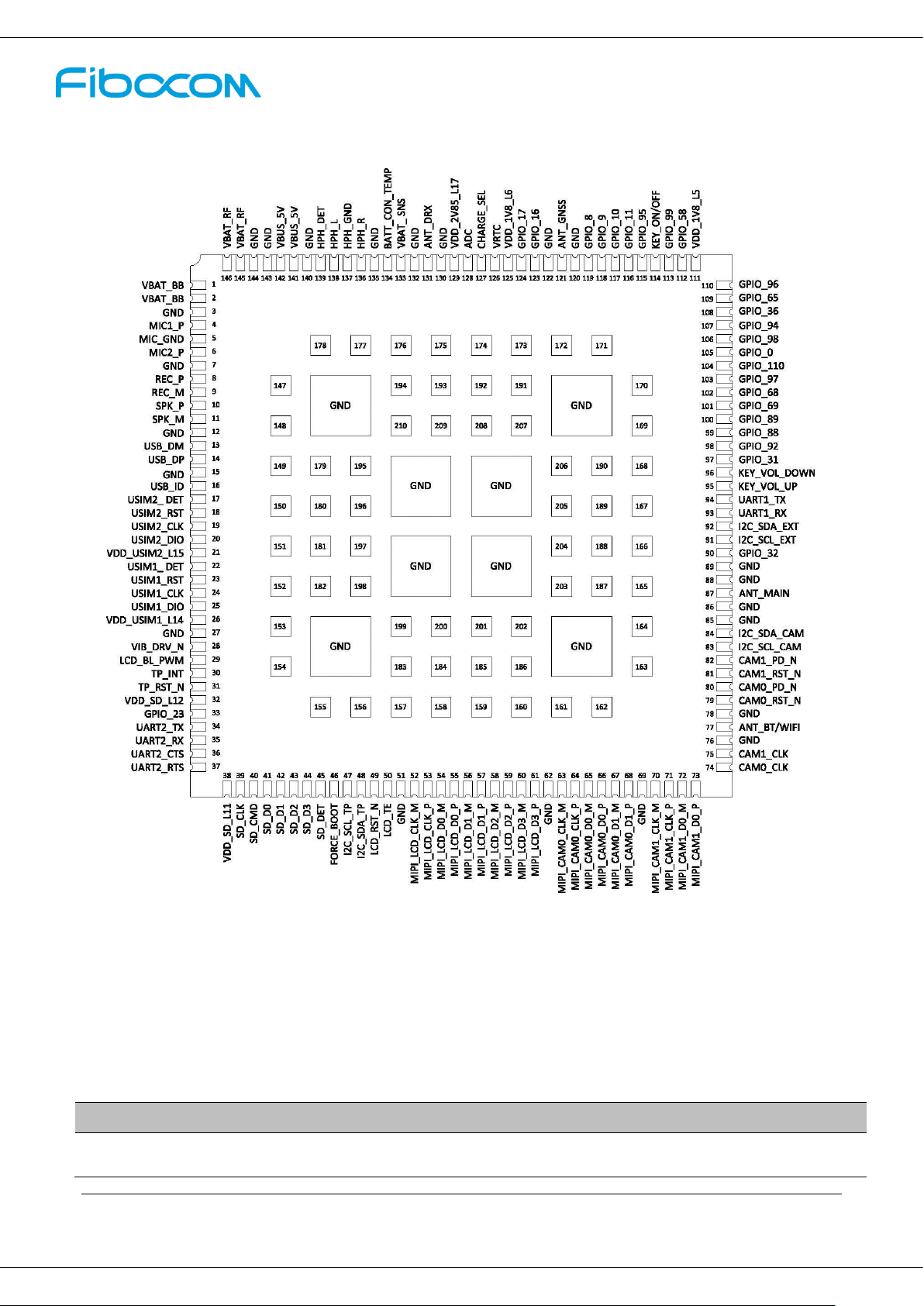
3.1.1 Pin Distribution
Figure2Pin Distribution (TOP perspective)
Note: The pin “NC” stands for No connect, ie the pin for this position is a reserved pin and does not need to be
connected.
3.1.2 Pin Definition
Table3I/O parameter definition
Type
Description
IO
input/output
The copyright of this document is owned by Fibocom Wireless Inc., and the document shall not be replicated without approval.
SC806Hardware User ManualPage18 of 70
DI
Digital input
DO
Digital output
PI
Power input
PO
Power output
AI
Analog input
AO
Analog output
OD
Open drain
The SC806’s pin functions and electrical characteristics are described in the following table:
Table4Pin description
Power
Pin Name
Pin No.
I/O
Pin Description
Note
VBAT_BB
1,2
PI
Baseband power input
Input voltage range: 3.3 ~ 4.5V, recommend
3.8V
VBAT_RF
145,146
PI
RF power input
Voltage range: 3.3 ~ 4.5V, recommend 3.8V
VDD_1V8_L5
111
PO
1.8Vvoltage output
Drive current200mA
VDD_1V8_L6
125
PO
1.8V voltage output
Drive current200mA
VDD_2V85_L17
129
PO
2.85V voltage output
Drive current420mA
VDD_SD_L12
32
PO
SD card pull-up resistor
power supply, 2.95V
Drive current50mA
VDD_SD_L11
38
PO
SD card power supply,
2.95V
Drive current600mA
VDD_USIM1_L14
26
PO
SIM card 1 power supply
2.95/1.8 Vadjustable, 55mA
VDD_ USIM2_L15
21
PO
SIM card 2 power supply
2.95/1.8 Vadjustable, 55mA
VRTC
126
I/O
RTC clock power supply
pin
Voltage range: 2.0 ~3.25V, recommend 3.0 V
GND
3,7,12,15,27,51,62,
Ground
The copyright of this document is owned by Fibocom Wireless Inc., and the document shall not be replicated without approval.
SC806Hardware User ManualPage19 of 70
69,76,78,85,86,88,
89,120,122,130,
132,135,140,143,
144,147,148,149,
150,160,161,162,
163,164,165,166,
167,168,169,170,
171,172,173,174,
175,176,177,178,
180,181,182,184,
185,186,188,189,
192,193,198,200,
201,208,209
Battery
Pin Name
Pin No.
I/O
Pin Description
Note
BATT_CON_TEMP
134
AI
Battery temperature
detection pin
NTC resistor connected to battery
VBAT_ SNS
133
AI
Battery voltage detection
pin
BATT_ID
194
AI
Battery position detection
CHARGE_SEL
127
DI
Charge scheme selection
pin
Grounding uses the module’s external charge
scheme, and floating uses the module’s
built-in charge scheme. Default is floating
VREF_BATT_THERM
187
AO
Battery temperature
detection circuit reference
voltage
LED_CHARGE_N
191
DI
Charge status indicator
pin
Connect indicator negative
Button
Pin Name
Pin No.
I/O
Pin Description
Note
KEY_ON/OFF
114
DI
Analog switch button
Low effect
The copyright of this document is owned by Fibocom Wireless Inc., and the document shall not be replicated without approval.
SC806Hardware User ManualPage20 of 70
KEY_VOL_UP
95
DI
Volume +
Low effect
KEY_VOL_DOWN
96
DI
Volume -
Low effect
KEY_RST_N
179
DI
Reset pin
PMIC reset input, low effect
USIM interface
Pin Name
Pin No.
I/O
Pin Description
Note
USIM1_DIO
25
I/O
SIM card 1 data signal
USIM1_CLK
24
DO
SIM card 1 clock signal
USIM1_RST
23
DO
SIM card 1 reset signal
USIM1_ DET
22
DI
SIM card 1 plug detection
Fixed level when not in use
USIM2_DIO
20
I/O
SIM card 2 data signal
USIM2_CLK
19
DO
SIM card 2 clock signal
USIM2_RST
18
DO
SIM card 2 reset signal
USIM2_ DET
17
DI
SIM card 2 plug detection
Fixed level when not in use
SDcard interface
Pin Name
Pin No.
I/O
Pin Description
Note
SD_D3
44
I/O
SD card data interface
SD_D2
43
I/O
SD card data interface
SD_D1
42
I/O
SD card data interface
SD_D0
41
I/O
SD card data interface
SD_CLK
39
DO
SD card clock
SD_CMD
40
I/O
SD cardcommand
interface
SD_DET
45
DI
SD card detection
Low level is effective
I2Cinterface
The copyright of this document is owned by Fibocom Wireless Inc., and the document shall not be replicated without approval.
SC806Hardware User ManualPage21 of 70
Pin Name
Pin No.
I/O
Pin Description
Note
I2C_SCL_EXT
91
I/O
I2Cclock
Sensor or other peripherals use
I2C_SDA_EXT
92
I/O
I2C data trace
Sensor or other peripherals use
I2C_SCL_TP
47
I/O
I2C clock
Default TP use
I2C_SDA_TP
48
I/O
I2C data trace
Default TP use
I2C_SCL_CAM
83
I/O
I2C clock
Default camera use
I2C_SDA_CAM
84
I/O
I2C data trace
Default camera use
USBinterface
Pin Name
Pin No.
I/O
Pin Description
Note
VBUS_5V
141,142
PI
Device mode, 5V input
USB_DM
13
I/O
USB signal -
USB_DP
14
I/O
USB signal +
USB_ID
16
AI
USB OTG detection pin
UARTinterface
Pin Name
Pin No.
I/O
Pin Description
Note
UART2_TX
34
DO
UART2 data transmission
UART2_RX
35
DI
UART2 data reception
UART2_CTS
36
DI
UART2clear transmission
UART2_RTS
37
DO
UART2request
UART1_TX
94
DO
UART1 data transmission
Debug port
UART1_RX
93
DI
UART1 data reception
Debugport
MIPI-DSIinterface
Pin Name
Pin No.
I/O
Pin Description
Note

The copyright of this document is owned by Fibocom Wireless Inc., and the document shall not be replicated without approval.
SC806Hardware User ManualPage22 of 70
MIPI_LCD_CLK_P
53
AO
MIPI differential clock
signal
MIPI_LCD_CLK_M
52
AO
MIPI_LCD_D3_P
61
AI/AO
MIPI differential data
signal
MIPI_LCD_D3_M
60
AI/AO
MIPI_LCD_D2_P
59
AI/AO
MIPI_LCD_D2_M
58
AI/AO
MIPI_LCD_D1_P
57
AI/AO
MIPI_LCD_D1_M
56
AI/AO
MIPI_LCD_D0_P
55
AI/AO
MIPI_LCD_D0_M
54
AI/AO
LCD_TE
50
DI
LCD refresh
Floating when not in use
LCD_RST_N
49
DO
LCD reset signal
LCD_BL_PWM
29
DO
LCD backlight PWM
control signal
MIPI-CSIinterface
Pin Name
Pin No.
I/O
Pin Description
Note
MIPI_CAM0_CLK_P
64
AI
Main camera MIPI
differential clock signal
MIPI_CAM0_CLK_M
63
AI
MIPI_CAM0_D1_P
68
AI/AO
Main camera MIPI
differential clock signal
MIPI_CAM0_D1_M
67
AI/AO
MIPI_CAM0_D0_P
66
AI/AO
MIPI_CAM0_D0_M
65
AI/AO

The copyright of this document is owned by Fibocom Wireless Inc., and the document shall not be replicated without approval.
SC806Hardware User ManualPage23 of 70
CAM0_CLK
74
DO
Main Camera main clock
CAM0_RST_N
79
DO
Main camera reset signal
CAM0_PD_N
80
DO
Main camera shutdown
MIPI_CAM1_CLK_P
71
AI
Auxiliary camera MIPI
differential clock signal
MIPI_CAM1_CLK_M
70
AI
MIPI_CAM1_D0_P
73
AI/AO
Auxiliary camera MIPI
differential data signal
MIPI_CAM1_D0_M
72
AI/AO
CAM1_CLK
75
DO
Auxiliary camera main
CAM1_RST_N
81
DO
Auxiliary camera reset
CAM1_PD_N
82
DO
Auxiliary camera
Touch interface
Pin Name
Pin No.
I/O
Pin Description
Note
TP_INT
30
DI
TP interruption signal
TP_RST_N
31
DO
TP reset signal
Audiointerface
Pin Name
Pin No.
I/O
Pin Description
Note
SPK_P
10
AO
External differential
output; class D power
amplifier
SPK_M
11
AO REC_P
8
AO
Receiver differential
output
REC_M
9
AO
HPH_L
138
AO
Headphone left channel
HPH_R
136
AO
Headphone right channel

The copyright of this document is owned by Fibocom Wireless Inc., and the document shall not be replicated without approval.
SC806Hardware User ManualPage24 of 70
MIC2_P
6
AI
Headphone MIC input
HPH_DET
139
AI
Headphone plug detect
HPH_GND
137 Headphone ground
MIC1_P
4
AI
Main MIC input
MIC_GND
5
GND
MIC ground
MIC3_P
195
AI
Auxiliary MIC input
MIC_BIAS1
210
AO
MIC offset reference
Only digital MIC uses it, so keep it floating
Antenna interface
Pin Name
Pin No.
I/O
Pin Description
Note
ANT_MAIN
87
I/O
2G/3G/4G main antenna
ANT_DRX
131
AI
Diversity receiving
ANT_BT/WIFI
77
I/O
WIFI/BTantenna
ANT_GNSS
121
AI
GNSS antenna
Module has built-in LNA with passive
Other interfaces
Pin Name
Pin No.
I/O
Pin Description
Note
VIB_DRV_N
28
PO
Motor drive pin
Connect to motor negative
FORCE_BOOT
46
DI
Forced pin
High level (1.8V) effect
ADC
128
AI
ADC detection pin
Input voltage range 0.1~4.5V
GPIO interface
Pin Name
Pin No.
I/O
Pin Description
Note
GPIO_0
105
I/O
Ordinary GPIO, 1.8V
power domain
B-PD:nppukp
GPIO_8
119
I/O
B-PD:nppukp
GPIO_9
118
I/O
B-PD:nppukp
GPIO_10
117
I/O
B-PD:nppukp

The copyright of this document is owned by Fibocom Wireless Inc., and the document shall not be replicated without approval.
SC806Hardware User ManualPage25 of 70
GPIO_11
116
I/O
B-PD:nppukp
GPIO_14
153
I/O
B-PD:nppukp
GPIO_15
197
I/O
B-PD:nppukp
GPIO_16
123
I/O
B-PD:nppukp
GPIO_17
124
I/O
B-PD:nppukp
GPIO_22
207
I/O
BH-PD:nppukp
GPIO_23
33
I/O
BH-PD:nppukp
GPIO_31
97
I/O
B-PD:nppukp
GPIO_32
90
I/O
B-PD:nppukp
GPIO_36
108
I/O
B-PD:nppukp
GPIO_58
112
I/O
B-PD:nppukp
GPIO_65
109
I/O
B-PD:nppukp
GPIO_68
102
I/O
B-PD:nppukp
GPIO_69
101
I/O
B-PD:nppukp
GPIO_88
99
I/O
B-PD:nppukp
GPIO_89
100
I/O
B-PD:nppukp
GPIO_92
98
I/O
B-PD:nppukp
GPIO_93
159
I/O
B-PU:nppdkp
GPIO_94
107
I/O
B-PD:nppukp
GPIO_95
115
I/O
B-PD:nppukp
GPIO_96
110
I/O
B-PD:nppukp
GPIO_97
103
I/O
B-PD:nppukp
GPIO_98
106
I/O
B-PD:nppukp
GPIO_99
113
I/O
B-PD:nppukp

The copyright of this document is owned by Fibocom Wireless Inc., and the document shall not be replicated without approval.
SC806Hardware User ManualPage26 of 70
GPIO_110
104
I/O
B-PD:nppukp
GPIO_1
190
I/O
B-PD:nppukp
GPIO_2
205
I/O
B-PD:nppukp
GPIO_3
203
I/O
B-PD:nppukp
PMU_GPIO_1
183
I/O
Ordinary GPIO,
adjustable power domain
1.2/1.8V
PMU_GPIO_2
202
I/O
PMU_GPIO_4
204
I/O
Ordinary GPIO,
adjustable power domain
1.2/1.8V/VBAT
Reserved pin
NC
151,152,154,155,156,157,1
58,196,199,206
Reserved pin
Floating by design
3.2 Power
The SC806 provides four VBAT pins for connecting to an external power: two VBAT_RF pins are used for the RF
power supply of the module, and two other VBAT_BB pins are used for baseband power supply of the module. The
power input range is from 3.3V to 4.5V, and the recommended value is 3.8V. The performance of the VBAT power,
such as load capacity, and ripple size, etc., will directly affect the performance and stability of the module. In
extreme cases, the module’s operating current can reach 2A, and if the power supply capacity is insufficient, the
voltage will drop. If the power voltage drops below 3.3V, the module may be powered off or restarted.
3.2.1 Power Supply
The SC806 module needs to be powered by the VBAT_BB/VBAT_RF pin
Table5Power supply parameters
Parameters
Minimum
Recommended
Maximum
Unit
VBAT_BB/VBAT_RF(DC)
3.3
3.8
4.5
V

The copyright of this document is owned by Fibocom Wireless Inc., and the document shall not be replicated without approval.
SC806Hardware User ManualPage27 of 70
Power design is shown as follows:
Figure 3Power Design
Power supply filter capacitor design is shown in the following table:
Table6Power supply filter capacitor design
Recommended
capacitor
Application
Description
220uF x 2
Regulating capacitor
Reduce power fluctuations during module
operation, requiring low ESR capacitor
LDO or DCDC power requires not less than 440uF
capacitor
Battery power can be properly reduced to 100 ~
220uF capacitor
1uF,100nF
Digital signal noise
Filter clock and digital signal interference
39pF,33pF
700, 850/900 MHz
Filter low band radio frequency interference
18pF,8.2pF,
6.8pF
1700/1800/1900,2100/2300,250
0/2600MH
Filter middle/high band radio frequency
interference
The power voltage drop example is shown in the figure:

The copyright of this document is owned by Fibocom Wireless Inc., and the document shall not be replicated without approval.
SC806Hardware User ManualPage28 of 70
Burst transmit Burst transmit
min:3.3V
VBAT
Ripple≤300mV
Drop
VBAT≥3.3V
Figure 4Power Voltage Drop Example
To ensure that the power voltage is not lower than 3.3V, it is recommended to connect two 220μF tantalum
capacitors with low ESR and filter capacitors of 1uF, 100nF, 39pF, and 33pF in parallel to the VBAT input of the
module. It is recommended that the PCB trace of VBAT be as short and wide as possible. Reduce the equivalent
impedance of the VBAT trace to ensure that at maximum output power, significant voltage drop will not occur at
high currents. It is recommended that the width of the VBAT trace should not be less than 2mm, and the longer and
the wider the trace, the ground plane of the power section should be more complete.
3.2.2 Lithium Battery Charge and Battery Management
If the SC806 is powered by a battery, it uses a lithium battery with temperature detection function. The SC806 has a
battery temperature detection function. The battery requires internal integration of a thermistor (default is 47K±1%,
B=4050 NTC), and the battery temperature detection pin is connected to the BATT_CON_TEMP pin (PIN 134).
SC806 has built-in linear charge management circuit that supports the charge of 3.7V lithium battery, and the use of
standard charger and non-standard charger for charge, with software automatic identification, standard charger
maximum charge current 1.44A, and non-standard charger limited charge current less than 500mA. The charge
process includes trickle charge, constant current charge, and constant voltage charge.
Trickle charge: it is divided into two parts. Trickle charge-A: charge current 90mA when the battery voltage is
lower than 2.8V; trickle charge-B: charge current 450mA when the battery voltage is between 2.8V~3.2V;
Constant current charge: constant current charge when the battery voltage is between 3.2V~4.2V. The current
is 1.44A when adapter is charging. The current is t 450mA when USB is charging;
Constant voltage charge: constant voltage charge when the battery voltage reaches 4.2V. The charge current is
gradually reduced, when the charge current is reduced to about 100mA, the charge is cut off.
3.2.3 RTC Power
VRTC is the power supply for the internal RTC clock of the module and can be used as a backup power for the
RTC clock. When the module power VBAT is powered on, the VRTC will output voltage. When there is no VBAT,

The copyright of this document is owned by Fibocom Wireless Inc., and the document shall not be replicated without approval.
SC806Hardware User ManualPage29 of 70
it needs to be powered by the external power. The button battery is generally used for power supply. The VRTC
parameters are as follows:
Table7VRTC parameters
Parameters
Minimum
Typical
Maximum
Unit
VRTC output voltage
2.5
3.1
3.2
V
VRTC input voltage (clock
normal)
2.0
3.0
3.25
V
VRTC input current (clock
normal)
5 10
uA
VRTC as RTC clock backup power reference design circuit is shown as follows:
Figure 5VRTC Reference Design Circuit Diagram
3.2.4 Power Output
The SC806 has multiple power outputs for peripheral circuits.
When applied, 33pF and 10pF capacitors can be connected in parallel to effectively remove high frequency
interference.
Table8Power description
Pin Name
Programmable Range (V)
Default Voltage (V)
Drive Current (mA)
VDD_1V8_L5
-
1.8
200
VDD_1V8_L6
-
1.8
200
VDD_2V85_L17
-
2.85
420
VDD_SD_L12
-
2.95
50

The copyright of this document is owned by Fibocom Wireless Inc., and the document shall not be replicated without approval.
SC806Hardware User ManualPage30 of 70
VDD_SD_L11
1.75~3.337
2.95
600
VDD_USIM1_L14
1.75~3.337
1.8/2.95
55
VDD_ USIM2_L15
1.75~3.337
1.8/2.95
55
3.3 Control Signal
The SC806 uses one control signal to startup/shutdown, restart, and sleep/wakeup the module.
Table9startup/shutdown pin definition
3.3.1 Module Startup
After VBAT is powered on, the module can be turned on by setting the KEY_ON/OFF signal low for more
than 2 seconds. The KEY_ON/OFF control reference diagram is as follows:
Figure 6Button Startup Circuit
Pin No.
Pin name
I/O
Description
Note
114
KEY_ON/OFF
DI
The default is high, and low is effective.
This pin can be used to startup/shutdown,
restart, and sleep/wakeup the module

The copyright of this document is owned by Fibocom Wireless Inc., and the document shall not be replicated without approval.
SC806Hardware User ManualPage31 of 70
Figure 7Drive Circuit Startup
Startup time slot is shown as follows:
Figure 8Startup Time Slot
3.3.2 Module Shutdown and Restart
After the SC806 is powered on, set the low KEY_ON/OFF signal to more than 500ms, the display interface will
pop up a selection box (select shutdown or restart). If it is greater than 10s, the system will be forced to shutdown.
Shutdown time slot is shown as follows:

The copyright of this document is owned by Fibocom Wireless Inc., and the document shall not be replicated without approval.
SC806Hardware User ManualPage32 of 70
Figure 9Shutdown Time Slot
3.3.3 Sleep/wakeup
During standby, set the KEY_ON/OFF signal low (100ms) and the system will go to sleep. The system supports
automatic sleep. The time from standby to sleep can be configured via software.
In sleep mode, the low KEY_ON/OFF signal can wake up the system.
3.3.4 Reset
KEY_RST_N is the reset output of the module PMIC. When the system crashes or other abnormalities occur, the
low KEY_RST_N signal is greater than 300ms, and the system will be forced to restart.
3.4 USBInterface
The SC806 supports one USB 2.0 interface, and supports two speed modes, full-speed (12Mbps) and high-speed
mode (480Mbps). USB supports OTG function and HUB expansion interface.
USB pin definition is shown in the following table:
Table10USB pin definition
Pin No.
Pin Name
I/O
Description
Note
141,142
VBUS_5V
PI
Device mode, 5V input
13
USB_DM
I/O
USB signal negative
14
USB_DP
I/O
USB signal positive
16
USB_ID
AI
USB OTG detection pin
The USB_VBUS power is a USB power or an adapter. It can be used as a USB plug-in detection and charge the

The copyright of this document is owned by Fibocom Wireless Inc., and the document shall not be replicated without approval.
SC806Hardware User ManualPage33 of 70
battery through the module’s internal PMU. The power input voltage range is 4.35~6.0V, and the recommended
value is 5V. The module supports single-cell lithium battery charge management. Different capacity models require
different charge parameters. The module’s built-in linear charge circuit supports up to 1.44A charge current.
The following is the USB interface circuit design:
Figure 10USB Interface Circuit Diagram
Note:
1) SC806 cannot output 5V DC internally, and 5V DC is required when USB is used as HOST.
2) ESD protection device for USB_DP/DM requires junction capacitance less than 1pF
3) USB_DP and USB_DM are high-speed differential signal traces. The highest transmission rate is 480Mbps.
Please pay attention to the following requirements in PCB layout:
USB_DP and USB_DM signal traces are required to be equal length and parallel, avoiding right-angle route,
and doing differential 90Ω impedance control
USB2.0 differential signal trace is laid on the nearest signal layer from the ground, and wrap ground
Table11module internal USB trace length
Pin No.
Pin name
Length (mm)
Length error (DP-DM)
13
USB_DM
28.70
-0.51
14
USB_DP
28.19
VBUS_5V
USB_DM
USB_DP
USB_ID
GND
GND
GND
GND
GND
USB_DM
USB_DP
USB_ID
VBUS_5V
1
2
3
4
5
Module
D2
C1
100nF
ESD
The copyright of this document is owned by Fibocom Wireless Inc., and the document shall not be replicated without approval.
SC806Hardware User ManualPage34 of 70
3.5 UARTInterface
The SC806 defines two UART interfaces and three I2Cs. It also supports multiplexed SPI. Please contact our
technical support when you need it.
The SC806 serial interface is 1.8V level. If the peripheral is at other levels, level shift is required.
Table12UART interface pin definition
Pin No.
Pin Name
I/O
Description
Note
34
UART2_TX
DO
UART2 data transmission
35
UART2_RX
DI
UART2 data reception
36
UART2_CTS
DI
UART2 clear transmission
37
UART2_RTS
DO
UART2 request transmission
94
UART1_TX
DO
UART1 data transmission, the
default is debug interface
93
UART1_RX
DI
UART1 data reception, the default
is debug interface
3.6 USIMInterface
The SC806 supports two SIM cards, dual-card dual standby (the software defaults is one card standby), and both
are hot pluggable (requires software configuration).
Table13USIM pin definition
Pin No.
Pin Name
I/O
Description
Note
26
VDD_USIM1_L14
PO
USIM1 power supply, 1.8V/2.95V
25
USIM1_DIO
I/O
USIM1 data signal
24
USIM1_CLK
DO
USIM1 clock signal
23
USIM1_RST
DO
USIM1 reset signal

The copyright of this document is owned by Fibocom Wireless Inc., and the document shall not be replicated without approval.
SC806Hardware User ManualPage35 of 70
22
USIM1_ DET
DI
USIM1 plug detection pin
20
USIM2_DIO
I/O
USIM2 data signal
19
USIM2_CLK
DO
USIM2 clock signal
18
USIM2_RST
DO
USIM2 reset signal
17
USIM2_ DET
DI
USIM2 detection pin
21
VDD_ USIM2_L15
PO
USIM2 power supply, 1.8V/2.95V
The USIM card interface reference circuit is as follows:
Figure 11USIM Card Interface Circuit Diagram
Note:
1) The length of the SC806 to the SIM card holder should be less than 100mm.
2) The layout and route of the SIM card must be kept away from EMI interference sources such as RF antenna and
digital switch signal.
Module
VDD_USIM
USIM_RST
USIM_CLK
USIM_DET
USIM_DIO
VCC
RST
CLK
IO
VPP
GND
DET
C1
33pF
`
C2
33pF
C3
33pF
100nF
C4
VDD_1V8_L5 VDD_USIM
D1
ESD
Close to USIM holder
USIM
Holder

The copyright of this document is owned by Fibocom Wireless Inc., and the document shall not be replicated without approval.
SC806Hardware User ManualPage36 of 70
3) The filter capacitance of the SIM card signal and the ESD device should be placed close to the card holder.
3.7 SDIO Interface
The SC806 supports one SDIO interface. The pin definition is as follows:
Table14SDIO pin definition
Pin No.
Pin Name
I/O
Description
Note
44
SD_D3
I/O
SD card data interface
43
SD_D2
I/O
SD card data interface
42
SD_D1
I/O
SD card data interface
41
SD_D0
I/O
SD card data interface
39
SD_CLK
DO
SD card clock
40
SD_CMD
I/O
SD card command interface
45
SD_DET
DI
SD card detection signal input
32
VDD_SD_L12
PO
as pull-up power for SD card data, clock,
and command trace, 1.8V/2.95V variable
38
VDD_SD_L11
PO
SD card power, 1.8V/2.95V variable
Note:
1) VDD_SD_L11 is the SD card peripheral driving power, and can provide about 600mA current. Pay attention to
the width of control trace.
2) Pull up SD card data, clock and command trace with VDD_SD_L12, and pull up SD_DET with VDD_SD_L5
3) SDIO, a high-speed digital signal trace needs to be shielded.
The copyright of this document is owned by Fibocom Wireless Inc., and the document shall not be replicated without approval.
SC806Hardware User ManualPage37 of 70
3.8 GPIO Interface
SC806 has many GPIO, and the interface level is 1.8V. The pin definition is as follows:
Table15GPIO list
Pin No.
Pin Name
Reset Status
Interruption Function
Wakeup Function
105
GPIO_0
B-PD:nppukp
Yes
No
119
GPIO_8
B-PD:nppukp
Yes
No
118
GPIO_9
B-PD:nppukp
Yes
No
117
GPIO_10
B-PD:nppukp
Yes
No
116
GPIO_11
B-PD:nppukp
Yes
Yes
153
GPIO_14
B-PD:nppukp
Yes
No
197
GPIO_15
B-PD:nppukp
Yes
No
123
GPIO_16
B-PD:nppukp
Yes
No
124
GPIO_17
B-PD:nppukp
Yes
No
207
GPIO_22
BH-PD:nppukp
Yes
No
33
GPIO_23
BH-PD:nppukp
Yes
No
97
GPIO_31
B-PD:nppukp
Yes
Yes
90
GPIO_32
B-PD:nppukp
Yes
No
108
GPIO_36
B-PD:nppukp
Yes
Yes
112
GPIO_58
B-PD:nppukp
Yes
Yes
109
GPIO_65
B-PD:nppukp
Yes
Yes
102
GPIO_68
B-PD:nppukp
Yes
No
101
GPIO_69
B-PD:nppukp
Yes
No
99
GPIO_88
B-PD:nppukp
Yes
No
100
GPIO_89
B-PD:nppukp
Yes
No

The copyright of this document is owned by Fibocom Wireless Inc., and the document shall not be replicated without approval.
SC806Hardware User ManualPage38 of 70
98
GPIO_92
B-PD:nppukp
Yes
Yes
159
GPIO_93
B-PU:nppdkp
Yes
No
107
GPIO_94
B-PD:nppukp
Yes
Yes
115
GPIO_95
B-PD:nppukp
Yes
Yes
110
GPIO_96
B-PD:nppukp
Yes
Yes
103
GPIO_97
B-PD:nppukp
Yes
Yes
106
GPIO_98
B-PD:nppukp
Yes
Yes
113
GPIO_99
B-PD:nppukp
Yes
No
104
GPIO_110
B-PD:nppukp
Yes
Yes
190
GPIO_1
B-PD:nppukp
Yes
No
205
GPIO_2
B-PD:nppukp
Yes
No
203
GPIO_3
B-PD:nppukp
Yes
No
Note
B: Bidirectional digital with CMOS input
H: High-voltage tolerant
NP:pdpukp = default no-pull with programmable options following the colon (:)
PD:nppukp = default pulldown with programmable options following the colon (:)
PU:nppdkp = default pullup with programmable options following the colon (:)
KP:nppdpu = default keeper with programmable options following the colon (:)
3.9 I2C Interface
The SC806 provides three I2Cs for TP, CAMERA, SENSOR, etc.. The I2C interface has a pull-up resistor of 10K
to VDD_1V8_L6 inside the module.
Table16I2C pin definition
Pin No.
Pin Name
I/O
Description
Note

The copyright of this document is owned by Fibocom Wireless Inc., and the document shall not be replicated without approval.
SC806Hardware User ManualPage39 of 70
91
I2C_SCL_EXT
I/O
Sensor or other peripheral
92
I2C_SDA_EXT
I/O
Sensor or other peripheral
47
I2C_SCL_TP
I/O
Default is TP
48
I2C_SDA_TP
I/O
Default is TP
83
I2C_SCL_CAM
I/O
Default is camera
84
I2C_SDA_CAM
I/O
Default is camera
3.10 ADC Interface
Table17ADC pin definition
Pin No.
Pin Name
I/O
Description
Note
128
ADC
AI
ADC detection pin
Input voltage range 0.1~4.5V
133
VBAT_ SNS
AI
Battery voltage detection pin
134
BATT_CON_TEMP
AI
Battery temperature detection
Connect to battery NTC resistor
3.11 Motor Drive Interface
The SC806 motor pin definition is as follows:
Table18Motor pin definition
Pin No.
Pin Name
I/O
Description
Note
28
VIB_DRV_N
PO
Motor drive pin
Connect to motor negative
3.12 LCM Interface
The SC806 video output interface is based on the MIPI_DSI standard and supports 4 sets high-speed differential

The copyright of this document is owned by Fibocom Wireless Inc., and the document shall not be replicated without approval.
SC806Hardware User ManualPage40 of 70
data transmission. The maximum speed of each set is up to 1.5Gbps, and it supports 720P.
Table19LCM pin definition
Pin No.
Pin Name
I/O
Description
Note
125
VDD_1V8_L6
PO
Power output
1.8V
129
VDD_2V85_L17
PO
Power output
2.85V
29
LCD_BL_PWM
DO
LCD backlight drive
49
LCD_RST_N
DO
LCD reset signal
50
LCD_TE
DI
LCD scan sync signal
52
MIPI_LCD_CLK_M
AO
LCD clock signal -
53
MIPI_LCD_CLK_P
AO
LCD clock signal +
61
MIPI_LCD_D3_P
AI/AO
LCD Lane 3 +
60
MIPI_LCD_D3_M
AI/AO
LCD Lane 3 -
59
MIPI_LCD_D2_P
AI/AO
LCD Lane 2 +
58
MIPI_LCD_D2_M
AI/AO
LCD Lane 2 -
57
MIPI_LCD_D1_P
AI/AO
LCD Lane 1 +
56
MIPI_LCD_D1_M
AI/AO
LCD Lane 1 -
55
MIPI_LCD_D0_P
AI/AO
LCD Lane 0 +
54
MIPI_LCD_D0_M
AI/AO
LCD Lane 0 -
3.13 Touch Screen Interface
The SC806 provides one set I2C interface that can be used to connect the touch screen (TP), and provides power
and interruption pin. The TP pin definition of the module is shown in the following table:
Table20TP pin definition
Pin No.
Pin Name
I/O
Description
Note

The copyright of this document is owned by Fibocom Wireless Inc., and the document shall not be replicated without approval.
SC806Hardware User ManualPage41 of 70
125
VDD_1V8_L6
PO
Power output
1.8V
129
VDD_2V85_L17
PO
Power output
2.85V
30
TP_INT
DI
TP interruption signal
31
TP_RST_N
DO
TP reset signal
47
I2C_SCL_TP
I/O
Touch screen I2C clock
48
I2C_SDA_TP
I/O
Touch screen I2C data
3.14 Camera Interface
The SC806 video input interface is based on the MIPI_CSI standard, and supports two cameras, and up to 8MP
pixel cameras.
MIPI-CSI0 is 2 Lane interface, and supports up to 8M Camera
MIPI-CSI1 is 1 Lane interface, and supports up to 5M Camera
3.14.1 Front camera
The front camera uses 1 set MIPI_CSI differential signal, and has been tested to support 2MP camera. The SC806
front camera pin definition is as follows:
Table21Front camera pin definition
Pin No.
Pin Name
I/O
Description
Note
125
VDD_1V8_L6
PO
Power output
1.8V
129
VDD_2V85_L17
PO
Power output
2.85V
71
MIPI_CAM1_CLK_P
AI
Front camera MIPI clock
signal +
70
MIPI_CAM1_CLK_M
AI
Front camera MIPI clock
signal -
73
MIPI_CAM1_D0_P
AI/AO
Front camera data signal
72
MIPI_CAM1_D0_M
AI/AO
Front camera data signal
75
CAM1_CLK
DO
Front camera main clock
81
CAM1_RST_N
DO
Front camera reset signal

The copyright of this document is owned by Fibocom Wireless Inc., and the document shall not be replicated without approval.
SC806Hardware User ManualPage42 of 70
82
CAM1_PD_N
DO
Front camera off signal
83
I2C_SCL_CAM
I/O
Camera I2C clock signal
84
I2C_SDA_CAM
I/O
Camera I2C data signal
3.14.2 Rear camera
Rear camera achieves transmission and control via the FPC and connector. The rear camera uses 2 sets MIPI_CSI
differential data trace interface, and has been tested to support 5MP camera. The SC806 rear camera pin definition
is as follows:
Table22Rear camera pin definition
Pin No.
Pin Name
I/O
Description
Note
125
VDD_1V8_L6
PO
Power output
1.8V
129
VDD_2V85_L17
PO
Power output
2.85V
64
MIPI_CAM0_CLK_P
AI
Rear camera MIPI Clock
Signal +
63
MIPI_CAM0_CLK_M
AI
Rear camera MIPI Clock
Signal -
68
MIPI_CAM0_D1_P
AI/AO
Rear camera data signal
67
MIPI_CAM0_D1_M
AI/AO
Rear camera data signal
66
MIPI_CAM0_D0_P
AI/AO
Rear camera data signal
65
MIPI_CAM0_D0_M
AI/AO
Rear camera data signal
74
CAM0_CLK
DO
Rear camera main clock
signal
79
CAM0_RST_N
DO
Rear camera reset signal
80
CAM0_PD_N
DO
Rear camera off signal
83
I2C_SCL_CAM
I/O
Camera I2C clock signal
84
I2C_SDA_CAM
I/O
Camera I2C data signal
3.14.3 Design note
MIPI DSI/CSI is a high-speed data trace. It has a relatively high requirement for routing, so priority should be

The copyright of this document is owned by Fibocom Wireless Inc., and the document shall not be replicated without approval.
SC806Hardware User ManualPage43 of 70
given to layout
The MIPI differential trace group must maintain parallel, equal length and impedance control of 100 ohms.
Do not use the ground trace in the MIPI trace group. The length is less than 100 mm. Ground wrap is needed.
Table23Module internal MIPI trace length
Pin No.
Pin Name
Length (mm)
Length Error (P-N)
53
MIPI_LCD_CLK_P
7.68
0
52
MIPI_LCD_CLK_M
7.68
61
MIPI_LCD_D3_P
9.05
0.57
60
MIPI_LCD_D3_M
8.48
59
MIPI_LCD_D2_P
7.72
0.09
58
MIPI_LCD_D2_M
7.63
57
MIPI_LCD_D1_P
7.74
0.21
56
MIPI_LCD_D1_M
7.53
55
MIPI_LCD_D0_P
7.79
-0.14
54
MIPI_LCD_D0_M
7.93
64
MIPI_CAM0_CLK_P
12.43
-0.06
63
MIPI_CAM0_CLK_M
12.49
68
MIPI_CAM0_D1_P
13.70
0.25
67
MIPI_CAM0_D1_M
13.45
66
MIPI_CAM0_D0_P
12.74
-0.16
65
MIPI_CAM0_D0_M
12.90
71
MIPI_CAM1_CLK_P
16.41
-0.10
70
MIPI_CAM1_CLK_M
16.51
73
MIPI_CAM1_D0_P
17.64
0.51
72
MIPI_CAM1_D0_M
17.13

The copyright of this document is owned by Fibocom Wireless Inc., and the document shall not be replicated without approval.
SC806Hardware User ManualPage44 of 70
3.15 Sensor Design
The SC806 communicates with sensors via I2C, and can support various types of sensors.
Table24Sensor control pin description
Pin No.
Pin Name
I/O
Description
Note
91
I2C_SCL_EXT
I/O
Sensor I2C clock signal
92
I2C_SDA_EXT
I/O
Sensor I2C data signal
3.16 Audio
3.16.1 Audio interface definition
SC806 supports analog audio interface, 3 inputs, 3 outputs, and does not support digital audio.
Table25Audio interface definition
Pin No.
Pin Name
I/O
Description
Note
10
SPK _P
AO
Out differential output; Class D
amplifier output
Maximum output 1W
11
SPK _M
AO
8
REC_P
AO
Handset differential output
9
REC_M
AO
138
HPH_L
AO
Headphone left channel output
136
HPH_R
AO
Headphone right channel output
6
MIC2_P
AI
Headphone MIC single-end input
139
HPH_DET
AI
Headphone detection signal input
137
HPH_GND
GND
Headphone ground
4
MIC1_P
AI
Main MIC single-end input
5
MIC_GND
GND
MIC ground

The copyright of this document is owned by Fibocom Wireless Inc., and the document shall not be replicated without approval.
SC806Hardware User ManualPage45 of 70
195
MIC3_P
AI
Auxiliary MIC single-end input
210
MIC_BIAS1
AO
MIC bias voltage
Note:
1) The MIC bias circuit has been added to the SC806 and no external addition is required.
2) Add 100K resistor to ground for MIC2_P
3) The SPK is a configured class D amplifier and cannot be connected to an external amplifier. It is recommended
to connect 8 ohm speakers. There is a high requirement for sound amplitude of loud speaker, and the amplifier can
be connected to the headphone for output.
4) Reduce noise and improve audio quality. The following approaches are recommended:
Keep audio PCB route away from the antenna and high-frequency digital signal
Reserve LC filter circuit in audio circuit to prevent EMC
Audio route need to be masked
4 Antenna Interface
The SC806 supports 2/3/4G main antenna/diversity receiving antenna, WIFI/BT antenna, and GNSS antenna.
4.1 MAIN/DRXAntenna
The SC806 provides two 2G/3G/4G antenna interfaces. The ANT_MAIN is used to receive and transmit RF
signal, and the ANT_DRX is used for diversity reception.
Table26MAIN/DRX antenna interface definition
Pin No.
Pin Name
I/O
Description
Note
87
ANT_MAIN
I/O
2G/3G/4G antenna interface
131
ANT_DRX
AI
Diversity reception antenna
4.1.1 Operating bands
Table27Module operating band
Band
Mode
Tx (MHz)
Rx (MHz)
Band 2
LTE FDD/WCDMA/GSM
1850-1910
1930-1990
Band 4
LTE FDD/WCDMA
1710-1755
2110-2155

The copyright of this document is owned by Fibocom Wireless Inc., and the document shall not be replicated without approval.
SC806Hardware User ManualPage46 of 70
Band 5
LTE FDD/WCDMA/GSM
824 - 849
869 - 894
Band 7
LTE FDD
2500-2570
2620-2690
Band 12
LTE FDD
699-716
729-746
Band 13
LTE FDD
746-756
777-787
Band 17
LTE FDD
704-716
734-746
4.1.2 Reference Design
For use of the SC806,the antenna pin and the RF connector or antenna feed point on the main board should be
connected via an RF trace. Microstrip trace is recommended for RF trace, with insertion loss within 0.2dB, and
impedance at 50ohm.
A π-type circuit is reserved between the SC806 and the antenna connector (or feed point) for antenna debugging.
Two parallel devices are directly connected across the RF trace and should not pull out a branch as the diagram
shows:
Figure 12MAIN/DRX Antenna Connection

The copyright of this document is owned by Fibocom Wireless Inc., and the document shall not be replicated without approval.
SC806Hardware User ManualPage47 of 70
4.2 WIFI/BTAntenna
Microstriptrace is recommended for the WIFI/BT RF route, with insertion loss within 0.2dB, and impedance at 50
ohms.
Table28WIFI/BT antenna interface definition
Pin No.
Pin Name
I/O
Description
Note
77
ANT_BT/WIFI
I/O
WIFI/BTantenna interface
4.2.1 Operating band
Table29WIFI/BT operating band
Mode
Frequency
unit
WIFI
2412~2472 /5180~5825
MHz
BT4.1
2402~2480
MHz
4.2.2 Reference design
WIFI/BT antenna connection reference design is shown as follows
Figure 13WIFI/BT Antenna Connection

The copyright of this document is owned by Fibocom Wireless Inc., and the document shall not be replicated without approval.
SC806Hardware User ManualPage48 of 70
4.3 GNSSAntenna
The following describes GNSS related information.
Table30GNSS antenna interface definition
Pin No.
Pin Name
I/O
Description
Note
121
ANT_GNSS
AI
GNSSantenna interface
4.3.1 Operating band
Table31GNSS operating band
Mode
Frequency
Unit
GPS
1575.42±1.023
MHz
GLONASS
1597.42-1605.8
MHz
BeiDou
1561.098±2.046
MHz
4.3.2 Reference design
4.3.2 Reference design
The SC806 has a built-in LNA. The passive antenna is used in the design of the device.
Microstriptrace is recommended for the GNSS RF route, with insertion loss within 0.2dB, and impedance at 50
ohms.
The connection reference design is shown as follows:

The copyright of this document is owned by Fibocom Wireless Inc., and the document shall not be replicated without approval.
SC806Hardware User ManualPage49 of 70
Figure 14GNSS Antenna Connection
4.4 Antenna Requirement
The SC806 module provides two antenna interfaces for the main set and diversity set. The antenna requirement is
shown in the following table:
Table32Module antenna requirement
SC806Module antenna requirement
Standard
Antenna requirements
GSM/WCDMA/CDMA/TDSCDMA/LTE
VSWR: ≤ 2
Gain (dBi):1
Max input power (W):50
Input impedance (Ω):50
Polarization type: vertical direction
Insertion loss:<1dB (700-900MHZ)
Insertion loss:< 1.5dB(1700-2100MHZ)
Insertion loss:< 2dB (2300-2600MHZ)
WIFI/BT
VSWR: ≤ 2
Gain (dBi):1
Max input power (W):50
nput impedance (Ω):50
Polarization type: vertical direction
Insertion loss:< 1dB
GNSS
frequency range:1559MHz~1607MHz
Polarization type: right-circular or linear polarization
VSWR: < 2 (typical)
Passive antenna gain: > 0dBi

The copyright of this document is owned by Fibocom Wireless Inc., and the document shall not be replicated without approval.
SC806Hardware User ManualPage50 of 70
5 Other Interfaces
For the application of other interfaces, please refer to the recommended design. If the application scenario and the
recommended design do not meet the requirements, please contact our technical personnel for confirmation.
6 RF PCB Layout Design Guide
For user PCB, the characteristic impedance of all RF signal traces should be at 50Ω. In general, the impedance of
the RF signal trace is determined by the dielectric constant of the material, the trace width (W), the ground
clearance (S), and the height of the reference ground plane (H). The control of the characteristic impedance of the
PCB is usually in two ways: microstriptrace and coplanar waveguide. To illustrate the design principles, the
following figures show the structure design of microstriptrace and coplanar waveguide when the impedance trace is
at 50Ω.
Microstriptrace complete structure
Figure 15Two-layer PCB Microstrip Structure
Coplanar waveguide complete structure

The copyright of this document is owned by Fibocom Wireless Inc., and the document shall not be replicated without approval.
SC806Hardware User ManualPage51 of 70
Figure 16Two-layer PCB Coplanar Waveguide Structure
Figure 17Four-layer PCB Coplanar Waveguide Structure (reference ground layer3)
Figure 18Four-layer PCB Coplanar Waveguide Structure (reference ground layer4)
In the design of RF antenna interface circuit, in order to ensure good performance and reliability of the RF signal, it
is recommended to follow the following principles in the circuit design:
➢ The impedance simulation tool should be used to accurately control the RF signal trace at 50Ω impedance.

The copyright of this document is owned by Fibocom Wireless Inc., and the document shall not be replicated without approval.
SC806Hardware User ManualPage52 of 70
➢ The GND pin adjacent to the RF pin should not have thermal welding plate and should be in full contact with
the ground.
➢ The distance between the RF pin and the RF connector should be as short as possible. At the same time, avoid
the right-angle route. The recommended route angle is 135 degrees.
➢ When connecting the device package, it should be noted that the signal pin must be kept away from the
ground.
➢ The reference ground plane of the RF signal trace should be complete; adding a certain amount of ground
holes around the signal and the reference ground can help improve the RF performance; the distance between
the ground hole and the signal trace should be at least 2 times the line width (2*W).
7 WIFI and Bluetooth
7.1.1 WIFI overview
The SC806 module supports 2.4G single-frequency WLAN wireless communication and 802.11b, 802.11g, and
802.11n standards, with a maximum speed up to 150 Mbps. Its characteristics are as follows:
➢ Support Wake-on-WLAN (WoWLAN)
➢ Support ad hoc mode
➢ Support WAPI
➢ Support AP mode
➢ Support Wi-Fi Direct
➢ Support MCS 0-7 for HT20 and HT40
7.1.2 WIFI performance parameters
Table33WIFI transmission power table
Frequency
Mode
Date
Rate
Bandwidth(
MHZ)
TXPower
(dBm)
EVM(dB)
IEEE
Spec(dB)
Mask
Margin(dB)
2.4G
802.11b
1Mbps
20
17.0±2
-21
-9
>5
11Mbps
20
17.0±2
-21
-9
>5
802.11g
6Mbps
20
16.0±2
-22
-5
>5

The copyright of this document is owned by Fibocom Wireless Inc., and the document shall not be replicated without approval.
SC806Hardware User ManualPage53 of 70
54Mbps
20
14.0±2
-31
-25
>5
802.11n
MCS0
20
15.0±2
-20
-5
>5
MCS7
20
13.0±2
-30
-27
>5
5G
802.11a
6Mbps
20
16.0±2
-22
-5
>5
54Mbps
20
13.0±2
-31
-25
>5
802.11n
MCS0
20
14.0±2
-23
-5
>5
MCS7
20
12.0±2
-30
-27
>5
Table34WIFI reception sensitivity
Frequenc
y
Mode
Date
Rate
Bandwidth(M
HZ)
Sensitivity(dBm)
IEEE Spec
(dBm)
Note
2.4G
802.11b
1Mbps
20
-91.0
-80
PER<8%
11Mbps
20
-90.0
-76
PER<8%
802.11g
6Mbps
20
-92.0
-82
PER<10%
54Mbps
20
-74.0
-65
PER<10%
802.11n
MCS0
20
-90.0
-82
PER<10%
MCS7
20
-72.0
-64
PER<10%
5G
802.11a
6Mbps
20
-89
-82
PER<10%
54Mbps
20
-72.0
-65
PER<10%
802.11n
MCS0
20
-88.0
-82
PER<10%
MCS7
20
-68.0
-64
PER<10%
The reference standards are as follows:
IEEE 802.11n WLAN MAC and PHY, October 2009 + IEEE 802.11-2007 WLAN MAC and PHY,June 2007
IEEE Std 802.11b, IEEE Std 802.11d, IEEE Std 802.11e, IEEE Std 802.11g, IEEE Std 802.11i:
IEEE 802.11-2007 WLAN MAC and PHY, June 2007

The copyright of this document is owned by Fibocom Wireless Inc., and the document shall not be replicated without approval.
SC806Hardware User ManualPage54 of 70
7.1.3 Bluetooth overview
The SC806 module supports BT4.1 (BR/EDR+BLE) standards. The modulation method supports GFSK, 8-DPSK
and π/4-DQPSK.BR/EDR. Channel bandwidth is 1MHz and can accommodate 79 channels. The BLE channel
bandwidth is 2MHz and can accommodate 40 channels. Its main characteristics are as follows:
➢ BT 4.1 + BR/EDR + BLE
➢ Support for ANT protocol
➢ Support for BT-WLAN coexistence operation, including optional concurrent receive
➢ Up to 3.5 piconets (master, slave, and page scanning)
Table35BT rate and version information
Version
Date Rate
Throughput
Note
BT1.2
1Mb/s
> 80Kbit/s
BT2.0+EDR
2Mb/s
> 80Kbit/s
BT3.0+HS
24Mbps
See3.0+HS
BT4.1 LE
24Mbps
See4.1 LE
The reference standards are as follows:
Bluetooth Radio Frequency TSS and TP Specification 1.2/2.0/2.0 + EDR/2.1/2.1+ EDR/3.0/3.0 +
HS, August 6, 2009
Bluetooth Low Energy RF PHY Test Specification, RF-PHY.TS/4.0.0, December 15, 2009
7.1.4 Bluetooth performance parameters
Table36BT performance parameters
Type
DH-5
2-DH5
3-DH5
Unit
Transmitter
11±1
10±1
10±1
dBm
Sensitivity
-93
-90
-86
dBm

The copyright of this document is owned by Fibocom Wireless Inc., and the document shall not be replicated without approval.
SC806Hardware User ManualPage55 of 70
8 GNSS
8.1.1 Overview
The SC806 smart module uses Qualcomm’s IZatTM engine. The GEN 8C also supports multi-positioning systems,
GPS, GLONASS and Beidou. The module is embedded with LNA, which can effectively improve the sensitivity of
GNSS.
8.1.2 Performance parameters
Table37GNSS positioning performance
Parameter
Description
Result
Unit
Sensitivity
Acquisition
-146
dBm
Tracking
-158
dBm
C/No
-130dBm
40
dB-Hz
TTFF
Cold Start
30
S
Warm Start
30
S
Hot Start 2 S
CEP
Static accuracy
5
m
9 Electrical Characteristics and Reliability
9.1 Recommended Parameters
Table38Recommended parameters
Parameter
Min
Nominal
Max
Unit
Vbat
3.3
3.8
4.5
V
USB_VBUS
4.35 5 6.0
V
VRTC
2.0
3.0
3.25
V
Operating
Temperature
-30
25
70
℃
Storage Temperature
-40
25
85
℃

The copyright of this document is owned by Fibocom Wireless Inc., and the document shall not be replicated without approval.
SC806Hardware User ManualPage56 of 70
9.2 Charge Parameters
Table39Charge parameters
Parameter
Min
Nominal
Max
Unit
Trickle Charge - A Current
81
90
99
mA
Trickle Charge - A threshold voltage (15.62mV Stepping)
2.5
2.796
2.984
V
Trickle Charge - B threshold voltage (18.75mV Stepping)
3.0
3.2
3.581
V
Charge voltage setting range (25mV stepping)
4
4.2
4.775
V
Charge voltage accuracy
/ / +/-2
%
Charge current setting range (90mA stepping)
90 / 1440
mA
Charge current accuracy
/ / +/-10
%
Charge cut-off current: when the charge current is set to
90mA to 450mA
/ 7 /
%
Charge cut-off current: when the charge current is set to
450mA to 1440mA
/
7.4 / %
9.3 Operating Current
Table40Operating current
Parameter
Description
Condition
Result
Unit
Ioff
Power Off
Power Off
10
uA
Isleep
WCDMA
DRX=8
3.44
mA
FDD LTE
DPC(DefaultPaging Cycle)=#256
2.33
Radio Off
AT+CFUN=4 Flight Mode
1.66

The copyright of this document is owned by Fibocom Wireless Inc., and the document shall not be replicated without approval.
SC806Hardware User ManualPage57 of 70
IWCDMA-RMS
WCDMA
RMS Current
Band2@ max power
463
Band4@ max power
479
Band5@ max power
432
ILTE-RMS
FDD data
RMS Current
Band2@max power(10MHz,1RB)
641
mA
mA
Band4@max power(10MHz,1RB)
615
Band5@max power(10MHz,1RB)
557
Band12@max power(10MHz,1RB)
618
Band13@max power(10MHz,1RB)
629
Band17@max power(10MHz,1RB)
622
9.4 RF Transmitting Power
The power transmitted by each frequency band of the SC806 module is shown in the following table:
Table41Module RF transmitting power
Mode
Band
Max Power(dBm)
Min Power(dBm)
WCDMA
Band II
23.5±1
<-50
Band IV
23.5±1
<-50
Band V
23.5±1
<-50
Band 2
23.0±1
<-44

The copyright of this document is owned by Fibocom Wireless Inc., and the document shall not be replicated without approval.
SC806Hardware User ManualPage58 of 70
Mode
Band
Max Power(dBm)
Min Power(dBm)
LTE FDD
Band 4
23.0±1
<-44
Band 5
23.0±1
<-44
Band 12
23.0±1
<-44
Band 13
23.0±1
<-44
Band 17
23.0±1
<-44
9.5 RF Receiver Sensitivity
The sensitivity of each frequency band of the SC806 module is shown in the following table:
Table42Module RF receiver sensitivity
Mode
Band
Primary
Diversity
PRX+Div
3GPP
Requirement
Unit
WCDMA
Band II
-110
NA
NA
-104.7
dBm
Band IV
-110
NA
NA
-106.7
dBm
Band V
-110
NA
NA
-104.7
dBm
LTE FDD(10M)
Band 2
-98
-99
-102
-95
dBm
Band 4
-98
-99
-102
-97
dBm
Band 5
-98
-99
-102
-95
dBm
Band 12
-98
-99
-102
-94
dBm
Band 13
-98
-99
-102
-94
dBm
Band 17
-98
-99
-102
-94
dBm
9.6 Electrostatic Protection
In the application of the module, due to static electricity generated by human body static electricity, and charged

The copyright of this document is owned by Fibocom Wireless Inc., and the document shall not be replicated without approval.
SC806Hardware User ManualPage59 of 70
friction between micro-electronics, etc., discharging to the module through various channels may cause certain
damage to the module, so ESD protection should be taken seriously. In the process of R&D, production assembly
and testing, and especially in product design, ESD protection measures should be taken. For example, anti-static
protection should be added at the interface of the circuit design and at the points susceptible to electrostatic
discharge or impact. Anti-static gloves should be worn during production.
ESD performance parameters Table 1-6 (Temperature: 25°C, Humidity: 45%)
Table43ESD performance
Test Point
Contact Discharge
Air Discharge
Unit
VBAT, GND
±5
±10
kV
Antenna interface
±4
±8
kV
Other interface
±0.5
±1
kV
10 Structural specification
10.1 Product appearance
The SC806 module appearance is shown in the figure:
Figure 19Module Product Appearance

The copyright of this document is owned by Fibocom Wireless Inc., and the document shall not be replicated without approval.
SC806Hardware User ManualPage60 of 70
10.2 Structural Dimension
The structural dimension of the SC806 module is shown in the figure:
Figure 20Structural Dimension

The copyright of this document is owned by Fibocom Wireless Inc., and the document shall not be replicated without approval.
SC806Hardware User ManualPage61 of 70
10.3 Recommended PCB Welding Plate Design
Figure 21Recommended PCB Welding Plate Design (Unit: mm)
10.4 SMT Patch
For module steel net design, please refer to SMT Application Design Instructions for the solder paste and furnace
temperature control.
10.5 Storage
10.5.1 Storage life
Storage conditions (recommended): temperature 23 ± 5 °C, relative humidity RH 35-70%.
Storage life (seal vacuum packaging): The Storage life is 12 months under the recommended storage conditions.

The copyright of this document is owned by Fibocom Wireless Inc., and the document shall not be replicated without approval.
SC806Hardware User ManualPage62 of 70
10.5.2 Workshop life
The workshop life of Level 3 moisture sensitive product is 72 hours. After unpacking, in the environment of
23±5°C workshop temperature and relative humidity less than 60%, the product should be returned to production or
other high-temperature operation within 72 hours, or stored in an environment with relative humidity less than 10%
to maintain dryness of the product.
10.5.3 Baking
Temperature:125±5℃
Continuous baking time: 24hours
Oven: convective heat exchange oven
10.6 Packaging
SC806module adopts tray sealed vacuum packaging, combined with the outer packaging method using the
hard carton box, so that the storage, transportation and the usage of modules can be protected to the greatest
extent.
Note:
The vacuum bag contains humidity card and desiccant. The module is a moisture-sensitive device, with
moisture sensitive level 3, and it is in line with the standards of theJEDEC. Please avoid permanent
damage to the product caused by moisture.
The module is a precision electronic product, and may suffer permanent damage if no correct electrostatic
protection measures are taken.
10.6.1 Tray packaging
The SC806 module is packaged in trays, 15 PCS per tray, 6 trays per box, 6 boxes per package. 1 tray of 10 PCS
modules is at above, and 1 empty tray is at the bottom, a tray with a total of 8 PCS. The tray packaging is shown in
the figure:

The copyright of this document is owned by Fibocom Wireless Inc., and the document shall not be replicated without approval.
SC806Hardware User ManualPage63 of 70
Figure 22Tray Packaging

The copyright of this document is owned by Fibocom Wireless Inc., and the document shall not be replicated without approval.
SC806Hardware User ManualPage64 of 70
10.6.2 Tray dimension
The tray dimension is 315*170*6.5mm, as shown in the figure:
Figure 23Tray Dimension

The copyright of this document is owned by Fibocom Wireless Inc., and the document shall not be replicated without approval.
SC806Hardware User ManualPage65 of 70
11 Appendix A Term Abbreviations
Terms
Description
AMR
Adaptive Multi-rate
bps
Bits Per Second
CS
Coding Scheme
DRX
Discontinuous Reception
EGSM
Extended GSM900 Band
FDD
Frequency Division Duplexing
GMSK
Gaussian Minimum Shift Keying
GSM
Global System for Mobile Communications
HSDPA
High Speed Down Link Packet Access
IMEI
International Mobile Equipment Identity
Imax
Maximum Load Current
LED
Light Emitting Diode
LSB
Least Significant Bit
LTE
Long Term Evolution
ME
Mobile Equipment
MS
Mobile Station
MT
Mobile Terminated
PCB
Printed Circuit Board
PDU
Protocol Data Unit
PSK
Phase Shift Keying
QAM
Quadrature Amplitude Modulation

The copyright of this document is owned by Fibocom Wireless Inc., and the document shall not be replicated without approval.
SC806Hardware User ManualPage66 of 70
QPSK
Quadrature Phase Shift Keying
RF
Radio Frequency
RHCP
Right Hand Circularly PolarizedRMS
RMS
Root Mean Square
RTC
Real Time Clock
Rx
Receive
SMS
Short Message Service
TDMA
Time Division Multiple Access
TE
Terminal Equipment
TX
Transmitting Direction
TDD
Time Division Duplexing
UART
Universal Asynchronous Receiver & Transmitter
UMTS
Universal Mobile Telecommunications System
URC
Unsolicited Result Code
(U)SIM
(Universal) Subscriber Identity Module
USSD
Unstructured Supplementary Service Data
Vmax
Maximum Voltage Value
Vnorm
Normal Voltage Value
Vmin
Minimum Voltage Value
VIHmax
Maximum Input High Level Voltage Value
VIHmin
Minimum Input High Level Voltage Value
VILmax
Maximum Input Low Level Voltage Value
VILmin
Minimum Input Low Level Voltage Value

The copyright of this document is owned by Fibocom Wireless Inc., and the document shall not be replicated without approval.
SC806Hardware User ManualPage67 of 70
VImax
Absolute Maximum Input Voltage Value
VImin
Absolute Minimum Input Voltage Value
VOHmax
Maximum Output High Level Voltage Value
VOHmin
Minimum Output High Level Voltage Value
VOLmax
Maximum Output Low Level Voltage Value
VOLmin
Minimum Output Low Level Voltage Value
VSWR
Voltage Standing Wave Ratio
WCDMA
Wideband Code Division Multiple Access

The copyright of this document is owned by Fibocom Wireless Inc., and the document shall not be replicated without approval.
SC806Hardware User ManualPage68 of 70
12 Appendix B GPRS Encoding Scheme
Table44GPRS encoding scheme
Encoding method
CS-1
CS-2
CS-3
CS-4
Rate
1/2
2/3
3/4
1
USF 3 3 3 3
Pre-coded USF
3 6 6
12
Radio Block excl.USF and BCS
181
268
312
428
BCS
40
16
16
16
Tail 4 4 4 -
Coded Bits
456
588
676
456
Punctured Bits
0
132
220
-
Data rate Kb/s
9.05
13.4
15.6
21.4

The copyright of this document is owned by Fibocom Wireless Inc., and the document shall not be replicated without approval.
SC806Hardware User ManualPage69 of 70
13 Appendix C GPRS Multislot
In the GPRS standard, 29 types of GPRS multislot modes are defined for use by mobile stations. The multislots
class defines the maximum rate of uplink and downlink. The expression is 3+1 or 2+2, the first number indicates
the number of downlink timeslots, and the second number indicates the number of uplink timeslots. Active
timeslots indicates the total number of timeslots that the GPRS device can use for both uplink and downlink
communications.
Table45Multilevel multislot allocation
Multislot Class
Downlink Slots
Uplink Slots
Active Slots 1 1
1 2 2
2
1 3 3
2
2
3
4
3
1
4
5
2
2
4
6
3
2 4 7
3
3 4 8
4
1
5
9
3
2
5
10
4
2
5
11
4
3
5
12
4
4 5 33
5
4
6

The copyright of this document is owned by Fibocom Wireless Inc., and the document shall not be replicated without approval.
SC806Hardware User ManualPage70 of 70
14 Appendix D EDGE Modulation and Encoding Method
Table46EDGE modulation and encoding method
Coding Scheme
Modulation
Coding Family
1 Timeslot
2 Timeslot
4 Timeslot
CS-1
GMSK
/
9.05kbps
18.1kbps
36.2kbps
CS-2
GMSK
/
13.4kbps
26.8kbps
53.6kbps
CS-3
GMSK
/
15.6kbps
31.2kbps
62.4kbps
CS-4
GMSK
/
21.4kbps
42.8kbps
85.6kbps
MCS-1
GMSK
C
8.80kbps
17.6kbps
35.2kbps
MCS-2
GMSK
B
11.2kbps
22.4kbps
44.8kbps
MCS-3
GMSK
A
14.8kbps
29.6kbps
59.2kbps
MCS-4
GMSK
C
17.6kbps
35.2kbps
70.4kbps
MCS-5
8-PSK
B
22.4kbps
44.8kbps
89.6kbps
MCS-6
8-PSK
A
29.6kbps
59.2kbps
118.4kbps
MCS-7
8-PSK
B
44.8kbps
89.6kbps
179.2kbps
MCS-8
8-PSK
A
54.4kbps
108.8kbps
217.6kbps
MCS-9
8-PSK
A
59.2kbps
118.4kbps
236.8kbps
 Loading...