


L830-EB Hardware User Manual
Lenovo Customization Version
Version: V1.0.0
Update date: 2017.07.04

Applicability Table
No. |
Product model |
Description |
|
|
|
1 |
L830-EB-02 |
NA |
|
|
|
Reproduction forbidden without Fibocom Wireless Inc. written authorization - All Rights Reserved.
L830-EB Hardware User Manual |
Page 2 of 41 |

Copyright
Copyright © 2017 Fibocom Wireless Inc. All rights reserved.
Without the prior written permission of the copyright holder, any company or individual is prohibited to excerpt, copy any part of or the entire document, or distribute the document in any form.
Notice
The document is subject to update from time to time owing to the product version upgrade or other reasons. Unless otherwise specified, the document only serves as the user guide. All the statements, information and suggestions contained in the document do not constitute any explicit or implicit guarantee.
Version Record
Version |
Update |
Remark |
V1.0.0 |
2017-07-04 |
Initial version |
|
|
|
Reproduction forbidden without Fibocom Wireless Inc. written authorization - All Rights Reserved.
L830-EB Hardware User Manual |
Page 3 of 41 |

Contents
1 |
Preface........................................................................................................................................... |
6 |
|
|
1.1 |
Introduction........................................................................................................................................... |
6 |
|
1.2 |
Reference Standard............................................................................................................................ |
6 |
|
1.3 Related Documents............................................................................................................................. |
6 |
|
2 |
Overview........................................................................................................................................ |
7 |
|
|
2.1 |
Introduction........................................................................................................................................... |
7 |
|
2.2 |
Specification.......................................................................................................................................... |
7 |
|
2.3 Application Framework........................................................................................................................ |
8 |
|
|
2.4 Hardware Framework.......................................................................................................................... |
9 |
|
3 |
Application Interface.................................................................................................................. |
9 |
|
|
3.1 |
M.2 Interface......................................................................................................................................... |
9 |
|
|
3.1.1 Pin Map............................................................................................................................................. |
10 |
|
|
3.1.2 Pin Definition..................................................................................................................................... |
11 |
|
3.2 Power Supply..................................................................................................................................... |
14 |
|
|
|
3.2.1 Power Supply................................................................................................................................... |
15 |
|
|
3.2.2 Logic level......................................................................................................................................... |
16 |
|
|
3.2.3 Power Consumption........................................................................................................................ |
16 |
|
3.3 |
Control Signal..................................................................................................................................... |
17 |
|
|
3.3.1 Module Start-Up............................................................................................................................... |
17 |
|
|
3.3.1.1 Start-up Circuit................................................................................................................................................ |
17 |
|
|
3.3.1.2 Start-up Timing Sequence............................................................................................................................ |
18 |
|
|
3.3.2 Module Shutdown............................................................................................................................ |
19 |
|
|
3.3.2.1 Software Shutdown........................................................................................................................................ |
19 |
|
|
3.3.2.2 Hardware Shutdown...................................................................................................................................... |
20 |
|
|
3.3.3 Module Reset................................................................................................................................... |
21 |
|
3.4 |
USB Interface..................................................................................................................................... |
22 |
|
|
3.4.1 USB Interface Definition................................................................................................................. |
22 |
|
|
3.4.2 USB Interface Application.............................................................................................................. |
22 |
|
3.5 |
USIM Interface................................................................................................................................... |
23 |
|
|
3.5.1 USIM Pins......................................................................................................................................... |
23 |
|
|
3.5.2 USIM Interface Circuit..................................................................................................................... |
23 |
|
|
3.5.2.1 N.C. SIM Card Slot........................................................................................................................................ |
23 |
|
|
3.5.2.2 N.O. SIM Card Slot........................................................................................................................................ |
24 |
|
|
3.5.3 USIM Hot-Plugging.......................................................................................................................... |
25 |
|
|
3.5.4 USIM Design.................................................................................................................................... |
25 |
Reproduction forbidden without Fibocom Wireless Inc. written authorization - All Rights Reserved.
L830-EB Hardware User Manual |
Page 4 of 41 |

|
3.6 |
Status Indicator.................................................................................................................................. |
26 |
|
|
3.6.1 LED#1 Signal.................................................................................................................................... |
26 |
|
|
3.6.2 WOWWAN#...................................................................................................................................... |
27 |
|
3.7 |
Interrupt Control................................................................................................................................. |
27 |
|
|
3.7.1 W_DISABLE1#................................................................................................................................. |
28 |
|
|
3.7.2 System Switch Control.................................................................................................................... |
28 |
|
|
3.7.3 Body SAR.......................................................................................................................................... |
28 |
|
3.8 |
Digital Audio........................................................................................................................................ |
29 |
|
|
3.8.1 I2S Mode........................................................................................................................................... |
29 |
|
|
3.8.2 PCM Mode........................................................................................................................................ |
30 |
|
3.9 |
I2C Interface Description.................................................................................................................. |
30 |
|
3.10 Clock Interface................................................................................................................................. |
31 |
|
|
3.11 Configuration Interface.................................................................................................................... |
31 |
|
|
3.12 Other Interfaces............................................................................................................................... |
32 |
|
4 |
Radio Frequency....................................................................................................................... |
32 |
|
|
4.1 |
RF Interface........................................................................................................................................ |
32 |
|
|
4.1.1 RF Interface Functionality.............................................................................................................. |
32 |
|
|
4.1.2 RF Connector Characteristic......................................................................................................... |
32 |
|
|
4.1.3 RF Connector Dimension............................................................................................................... |
32 |
|
4.2 |
Operating Band.................................................................................................................................. |
34 |
|
4.3 Transmitting Power............................................................................................................................ |
34 |
|
|
4.4 |
Receiver Sensitivity........................................................................................................................... |
35 |
|
4.5 GNSS................................................................................................................................................... |
35 |
|
|
4.6 Antenna Design.................................................................................................................................. |
36 |
|
5 |
Structure Specification............................................................................................................ |
37 |
|
|
5.1 |
Product Appearance.......................................................................................................................... |
37 |
|
5.2 |
Dimension of Structure..................................................................................................................... |
37 |
|
5.3 |
M.2 Interface Model........................................................................................................................... |
38 |
|
5.4 |
M.2 Connector.................................................................................................................................... |
38 |
|
5.5 |
Storage................................................................................................................................................ |
39 |
|
|
5.5.1 Storage Life...................................................................................................................................... |
39 |
|
5.6 |
Packing................................................................................................................................................ |
39 |
|
|
5.6.1 Tray Package.................................................................................................................................... |
40 |
|
|
5.6.2 Tray size............................................................................................................................................ |
41 |
Reproduction forbidden without Fibocom Wireless Inc. written authorization - All Rights Reserved.
L830-EB Hardware User Manual |
Page 5 of 41 |

1 Preface
1.1 Introduction
The document describes the electrical characteristics, RF performance, dimensions and application environment, etc. of L830-EB (hereinafter referred to as L830). With the assistance of the document and other instructions, the developers can quickly understand the hardware functions of L830 modules and develop products.
1.2 Reference Standard
The design of the product complies with the following standards:
3GPP TS 34.121-1 V10.8.0: User Equipment (UE) conformance specification;Radio transmission and reception (FDD);Part 1: Conformance specification
3GPP TS 36.521-1 V10.6.0: User Equipment (UE) conformance specification; Radio transmission and reception; Part 1: Conformance testing
3GPP TS 21.111 V10.0.0: USIM and IC card requirements
3GPP TS 51.011 V4.15.0: Specification of the Subscriber Identity Module -Mobile Equipment (SIM-ME) interface
3GPP TS 31.102 V10.11.0: Characteristics of the Universal Subscriber Identity Module (USIM) application
3GPP TS 31.11 V10.16.0: Universal Subscriber Identity Module (USIM) Application Toolkit(USAT)
3GPP TS 36.124 V10.3.0: ElectroMagnetic Compatibility (EMC) requirements for mobile terminals and ancillary equipment
3GPP TS 27.007 V10.0.8: AT command set for User Equipment (UE)
PCI_Express_M.2_Specification_Rev1.1
1.3Related Documents
RF Antenna Application Design Specification
L8-Family System Driver Integration and Application Guidance
L8-Family AT Commands Manual
Reproduction forbidden without Fibocom Wireless Inc. written authorization - All Rights Reserved.
L830-EB Hardware User Manual |
Page 6 of 41 |

RF_067, Issue 01
EU Regulator Conformance
Hereby, We, Fibocom Wireless Inc. declares that the radio equipment type L830-EB is in compliance with the Directive 2014/53/EU.
In all cases assessment of the final product must be mass against the Essential requirements of the Directive 2014/53/EU Article 3.1(a) and (b), safety and EMC respectively, as well as any relevant Article 3.2 requirements.
External antenna is used with the module during the testing process, the maximum antenna gain for frequency < 1G is 3dBi, for frequency > 1G is 5dBi and the antenna separation distance is 20cm.
EU Declaration of Conformity (DoC) Hereby,
Name of manufacturer: |
Fibocom Wireless Inc. |
|
5/F, Tower A, Technology Building II, 1057 Nanhai Blvd, |
Address: |
Nanshan, |
City: |
Shenzhen, |
Country: |
China |
declares that the DoC is issued under its sole responsibility and that this product:
Product description: |
LTE module |
|
Type designation(s): |
L830-EB |
|
Trademark: |
Fibocom |
|
Product Identification |
|
|
Element |
|
L830-EB |
is in conformity with the relevant Union harmonization legislation:
Radio Equipment directive: 2014 / 53 / EU.
with reference to the following standards applied:
1.Health (Article 3.1(a) of Directive 2014/53/EU)
Applied Standard(s):
EN 62311 : 2008
2.Safety (Article 3.1(a) of Directive 2014/53/EU)
Applied Standard(s):
EN 60950-1: 2006 + A11: 2009 + A1: 2010 + A12: 2011 + A2: 2013
3.Electromagnetic compatibility (Article 3.1 (b) of Directive 2014/53/EU)
Applied Standard(s):
Draft EN 301 489-1 V2.2.0 / -52 V1.1.0 / Final Draft EN301489-3 V2.1.1
4.Radio frequency spectrum usage (Article 3.2 of Directive 2014/53/EU)
Applied Standard(s):
EN 301 908-1 V11.1.1 / -2 V11.1.1 / -13 V11.1.1
EN 303 413 V1.1.1
The Notified Body SIEMIC INC. with Notified Body number 2200 performed:
Modules: B+C and issued the EU-type examination certificate.
Signed for and on behalf of:
Date: |
August 21, 2017 |
|
City: |
Shenzhen, |
|
Name: |
Bond Yuan |
|
Title: |
Certification Engineer |
|
Signature: |
|
|
Federal Communication Commission Interference Statement
This device complies with Part 15 of the FCC Rules. Operation is subject to the following two conditions: (1) This device may not cause harmful interference, and (2) this device must accept any interference received, including interference that may cause undesired operation.
This equipment has been tested and found to comply with the limits for a Class B digital device, pursuant to Part 15 of the FCC Rules. These limits are designed to provide reasonable protection against harmful interference in a residential installation. This equipment generates, uses and can radiate radio frequency energy and, if not installed and used in accordance with the instructions, may cause harmful interference to radio communications. However, there is no guarantee that interference will not occur in a particular installation. If this equipment does cause harmful interference to radio or television reception, which can be determined by turning the equipment off and on, the user is encouraged to try to correct the interference by one of the following measures:
Reorient or relocate the receiving antenna.
Increase the separation between the equipment and receiver.
Connect the equipment into an outlet on a circuit different from that to which the receiver is connected.
Consult the dealer or an experienced radio/TV technician for help.
FCC Caution:
Any changes or modifications not expressly approved by the party responsible for compliance could void the user's authority to operate this equipment.
This transmitter must not be co-located or operating in conjunction with any other antenna or transmitter.
Radiation Exposure Statement:
This equipment complies with FCC radiation exposure limits set forth for an uncontrolled environment. This equipment should be installed and operated with minimum distance 20cm between the radiator & your body.
This device is intended only for OEM integrators under the following conditions:
1)External antenna is used with the module during the testing process, the maximum antenna gain for frequency<1G is 3dBi, for frequency>1G is 5 dBi and the antenna separation distance is 20cm.
2)The transmitter module may not be co-located with any other transmitter or antenna.
As long as 2 conditions above are met, further transmitter test will not be required. However, the OEM integrator is still responsible for testing their end-product for any additional compliance requirements required with this module installed
IMPORTANT NOTE: In the event that these conditions can not be met (for example certain laptop configurations or co-location with another transmitter), then the FCC authorization is no longer considered valid and the FCC ID can not be used on the final product. In these circumstances, the OEM integrator will be responsible for re-evaluating the end product (including the transmitter) and obtaining a separate FCC authorization.
End Product Labeling
This transmitter module is authorized only for use in device where the antenna may be installed such that 20 cm may be maintained between the antenna and users. The final end product must be labeled in a visible area with the following: Contains FCC ID: ZMOL830EB The grantee's FCC ID can be used only when all FCC compliance requirements are met.
Manual Information To the End User
The OEM integrator has to be aware not to provide information to the end user regarding how to install or remove this RF module in the user’s manual of the end product which integrates this module. The end user manual shall include all required regulatory information/warning as show in this manual.

2 Overview
2.1 Introduction
The L830 is a highly integrated 4G cellular module which uses the standard PCIe M.2 interface.It supports LTE FDD/WCDMA mode cellular communication.
2.2 Specification
Specification |
|
|
|
|
|
|
|
|
|
|
|
||
|
LTE FDD: Band 1,3,5,7,8,20,28 |
|||||
|
|
|
|
|
||
Operating Band |
WCDMA/HSPA+: Band I, V, VIII |
|||||
|
|
|
|
|
|
|
|
GPS/GLONASS: L1 |
|
|
|
||
|
|
|
|
|
|
|
|
|
|
|
1 +3,5,7,20 |
|
|
|
|
|
|
|
|
|
|
LTE inter-band CA |
|
3 +5,7,8,20,28 |
|
||
CA |
|
|
|
|||
|
5 +7 |
|
||||
|
|
|
|
|||
|
|
|
|
|
|
|
|
|
|
|
7 +20,28 |
|
|
|
|
|
|
|
|
|
|
LTE intra-band CA |
|
3,7 |
|
||
|
|
|
|
|
|
|
Data |
LTE FDD |
|
300Mbps DL/50Mbps UL(Cat 6) |
|||
|
|
|
|
|
||
|
|
|
UMTS:384 kbps DL/384 kbps UL |
|||
Transmission |
UMTS/HSPA+ |
|
|
|||
|
|
|
|
|||
|
|
DC-HSDPA+:42Mbps DL(Cat 24)/5.76Mbps UL(Cat6) |
||||
|
|
|
|
|||
|
|
|
|
|||
Power Supply |
DC 3.135V 4.4V, Typical 3.3V |
|||||
|
|
|
|
|||
|
Normal Operating temperature -10°C +55°C |
|||||
Temperature |
Extended Operating temperature -30°C +65°C |
|||||
|
|
|
|
|||
|
Storage temperature -40°C +85°C |
|||||
|
|
|
|
|
||
Physical |
Interface: M.2 Key-B |
|
|
|
||
|
|
|
|
|
||
Dimension 30 x 42 x 2.3mm |
||||||
characteristics |
||||||
|
|
|
|
|
||
Weight: About 5.8 g |
|
|
|
|||
|
|
|
|
|||
|
|
|
|
|
||
WCDMA Band 1/8 |
24dBm |
|
|
|
||
|
|
|
|
|
||
LTE Band 1/3/7/8/20 |
23dBm |
|
|
|
||
|
|
|
|
|
|
|
|
|
|
|
|
|
|
Interface |
|
|
|
|
|
|
|
|
|
|
|
||
Antenna Connector |
WWAN Main Antenna x 1 |
|||||
|
|
|
|
|
||
WWAN Diversity(GNSS AUX) Antenna x 1 |
||||||
|
||||||
|
|
|
|
|
||
|
|
|
|
|
|
|
Reproduction forbidden without Fibocom Wireless Inc. written authorization - All Rights Reserved. |
||||||
L830-EB Hardware User Manual |
|
Page 7 of 41 |
||||
USIM 3V/1.8V
USB 2.0 x 1
I2S
Function Interface
I2C
EINT System Indicator
Clock
Software
Protocol Stack |
IPV4/IPV6 |
|
|
AT commands |
3GPP TS 27.007 and 27.005, and proprietary FIBOCOM AT commands |
|
|
Firmware update |
USB |
|
|
Note
When the temperature goes beyond the normal operating temperature range of -10°C~+55°C, the RF performance of the module may be slightly off 3GPP specifications.
2.3 Application Framework
The peripheral applications for L830 module are shown in Figure 2-1:
Figure2-1 Application Framework
Reproduction forbidden without Fibocom Wireless Inc. written authorization - All Rights Reserved.
L830-EB Hardware User Manual |
Page 8 of 41 |
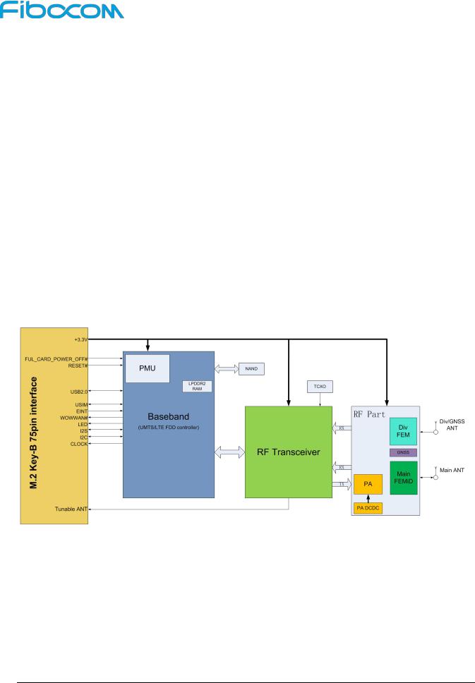
2.4 Hardware Framework
The hardware framework in Figure 2-2 shows the main hardware functions of L830 module, including baseband and RF functions.
Baseband contains the followings:
UMTS/LTE FDD controller/Power supply
NAND/internal LPDDR2 RAM
Application interface
RF contains the followings:
RF Transceiver
RF Power/PA
RF Front end
RF Filter
Antenna Connector
Figure 2-2 Hardware Framework
3 Application Interface
3.1 M.2 Interface
The L830 module uses standard M.2 Key-B interface, with a total of 75 pins.
Reproduction forbidden without Fibocom Wireless Inc. written authorization - All Rights Reserved.
L830-EB Hardware User Manual |
Page 9 of 41 |

3.1.1 Pin Map
Figure 3-1 Pin Map
Note:
Pin “Notch” represents the gap of the gold fingers.
Reproduction forbidden without Fibocom Wireless Inc. written authorization - All Rights Reserved.
L830-EB Hardware User Manual |
Page 10 of 41 |

3.1.2 Pin Definition
The pin definition is as follows:
Pin |
Pin Name |
I/O |
Reset |
Pin Description |
Type |
Value |
|||||
|
|
|
|
Connected to internal GND, L830 |
|
1 |
CONFIG_3 |
O |
L |
M.2 module is configured as the |
|
|
|
|
|
WWAN-SSIC 0 interface type. |
|
|
|
|
|
|
|
2 |
+3.3V |
PI |
|
Module main power input. |
Power Supply |
|
|
|
|
|
|
3 |
GND |
|
|
GND |
Power Supply |
|
|
|
|
|
|
4 |
+3.3V |
PI |
|
Module main power input. |
Power Supply |
|
|
|
|
|
|
5 |
GND |
|
|
GND |
Power Supply |
|
|
|
|
|
|
6 |
FULL_CARD_POWER_OFF# |
I |
|
Power on/off control signal,active |
CMOS |
|
High. |
3.3/1.8V |
|||
|
|
|
|
||
|
|
|
|
|
|
7 |
USB D+ |
I/O |
|
USB 2.0 D+ signal |
0.3---3V |
|
|
|
|
|
|
8 |
W_DISABLE1# |
I |
PU |
WWAN Disable, active low. |
CMOS 3.3V |
|
|
|
|
|
|
9 |
USB D- |
I/O |
|
USB 2.0 D- signal |
0.3---3V |
|
|
|
|
|
|
10 |
LED1# |
O |
OD |
System status LED, drain output. |
CMOS 3.3V |
|
|
|
|
|
|
11 |
GND |
|
|
GND |
Power Supply |
|
|
|
|
|
|
12 |
Notch |
|
|
Notch |
|
|
|
|
|
|
|
13 |
Notch |
|
|
Notch |
|
|
|
|
|
|
|
14 |
Notch |
|
|
Notch |
|
|
|
|
|
|
|
15 |
Notch |
|
|
Notch |
|
|
|
|
|
|
|
16 |
Notch |
|
|
Notch |
|
|
|
|
|
|
|
17 |
Notch |
|
|
Notch |
|
|
|
|
|
|
|
18 |
Notch |
|
|
Notch |
|
|
|
|
|
|
|
19 |
Notch |
|
|
Notch |
|
|
|
|
|
|
|
20 |
I2S_CLK |
O |
PD |
I2S serial clock |
CMOS 1.8V |
|
|
|
|
|
|
|
|
|
|
Not connected, L830 M.2 module is |
|
21 |
CONFIG_0 |
O |
NC |
configured as the WWAN-SSIC 0 |
|
|
|
|
|
interface type. |
|
|
|
|
|
|
|
22 |
I2S_RX |
I |
PD |
I2S serial data input |
CMOS 1.8V |
|
|
|
|
|
|
|
|
|
|
|
|
|
Reproduction forbidden without Fibocom Wireless Inc. written authorization - All Rights Reserved. |
||||
L830-EB Hardware User Manual |
|
|
|
Page 11 of 41 |
|
 Loading...