


FIBOCOM_L860-GL
Hardware User Manual
Version 1.0.2
Date 2018-07-28

Copyright
Copyright © 2018 Fibocom Wireless Inc. All rights reserved.
Without the prior written permission of the copyright holder, any company or individual is prohibited to excerpt, copy any part of or the entire document, or distribute the document in any form.
Notice
changes or modifications not expressly approved by the party responsible for compliance could void the user’s authority to operate the equipment.
This equipment has been tested and found to comply with the limits for a Class B digital device, pursuant to Part 15 of the FCC Rules. These limits are designed to provide reasonable protection against harmful interference in a residential installation. This equipment generates, uses and can radiate radio frequency energy and, if not installed and used in accordance with the instructions, may cause harmful interference to radio communications. However, there is no guarantee that interference will not occur in a particular installation.
If this equipment does cause harmful interference to radio or television reception, which can be determined by turning the equipment off and on, the user is encouraged to try to correct the interference by one or more of the following measures:
--Reorient or relocate the receiving antenna.
--Increase the separation between the equipment and receiver.
--Connect the equipment into an outlet on a circuit different from that to which the receiver is connected.
--Consult the dealer or an experienced radio/TV technician for help.
This equipment complies with FCC radiation exposure limits set forth for an uncontrolled environment. End user must follow the specific operating instructions for satisfying RF exposure compliance. This transmitter must not be co-located or operating in conjunction with any other antenna or transmitter.
This device complies with Part 15 of the FCC Rules. Operation is subject to the following two conditions: (1) this device may not cause harmful interference, and (2) this device must accept any interference received, including interference that may cause undesired operation.
The document is subject to update from time to time owing to the product version upgrade or other reasons. Unless otherwise specified, the document only serves as the user guide. All the statements, information and suggestions contained in the document do not constitute any explicit or implicit guarantee.
Reproduction forbidden without Fibocom Wireless Inc. written authorization - All Rights Reserved.
FIBOCOM_L860-GL Hardware User Manual |
Page 2 of 55 |

This device is intended only for OEM integrators under the following conditions:
1) The antenna must be installed such that 20 cm is maintained between the antenna and users, and the Max allowed
antenna gain is as following table showed:
Operating Band |
Antenna Gain dBi |
|
|
WCDMA BAND II |
8.5 |
|
|
WCDMA BAND IV |
5.5 |
|
|
WCDMA BAND V |
9.07 |
|
|
LTE BAND 2 |
9 |
|
|
LTE BAND 4 |
6 |
|
|
LTE BAND 5 |
9.41 |
|
|
LTE BAND 7 |
9 |
|
|
LTE BAND 12 |
8.85 |
|
|
LTE BAND 13 |
10.31 |
|
|
LTE BAND 14 |
10.38 |
|
|
LTE BAND 17 |
9.74 |
|
|
LTE BAND 25 |
9 |
|
|
LTE BAND 26 814-824 |
8.51 |
|
|
LTE BAND 26 824-849 |
8.56 |
LTE BAND 30 |
1 |
|
|
LTE BAND 38 |
9 |
|
|
LTE BAND 41 |
5.5 |
|
|
LTE BAND 66 |
6 |
|
|
2) The transmitter module may not be co-located with any other transmitter or antenna.
As long as 2 conditions above are met, further transmitter test will not be required. However, the OEM integrator is still responsible for testing their end-product for any additional compliance requirements required with this module installed
Host manufacturer is responsible for ensuring that the host continues to be compliant with the Part 15 subpart B unintentional radiator requirements after the module is installed and operational.
Reproduction forbidden without Fibocom Wireless Inc. written authorization - All Rights Reserved.
FIBOCOM_L860-GL Hardware User Manual |
Page 3 of 55 |

The document is subject to update from time to time owing to the product version upgrade or other reasons. Unless otherwise specified, the document only serves as the user guide. All the statements, information and suggestions contained in the document do not constitute any explicit or implicit guarantee.
IMPORTANT NOTE: In the event that these conditions can not be met (for example certain laptop configurations or co-location with another transmitter), then the FCC authorization is no longer considered valid and the FCC ID can not be used on the final product. In these circumstances, the OEM integrator will be responsible for re-evaluating the end product (including the transmitter) and obtaining a separate FCC authorization.
End Product Labeling
This transmitter module is authorized only for use in device where the antenna may be installed such that 20 cm may be maintained between the antenna and users. The final end product must be labeled in a visible area with the following: “Contains FCC ID: ZMOL860GL”. The grantee's FCC ID can be used only when all FCC compliance requirements are met.
Manual Information To the End User
The OEM integrator has to be aware not to provide information to the end user regarding how to install or remove this RF module in the user’s manual of the end product which integrates this module. The end user manual shall include all required regulatory information/warning as show in this manual.
Reproduction forbidden without Fibocom Wireless Inc. written authorization - All Rights Reserved.
FIBOCOM_L860-GL Hardware User Manual |
Page 4 of 55 |

This device complies with Industry Canada license-exempt RSS standard(s). Operation is subject to the following two conditions: (1) this device may not cause interference, and (2) this device must accept any interference, including interference that may cause undesired operation of the device.
Le présent appareil est conforme aux CNR d'Industrie Canada applicables aux appareils radio exempts de licence. L'exploitation est autorisée aux deux conditions suivantes : (1) l'appareilne doit pas produire de brouillage, et (2) l'utilisateur de l'appareil doit accepter tout brouillage radioélectrique subi, même si le brouillage est susceptible d'en compromettre le fonctionnement.
Radiation Exposure Statement:
This equipment complies with IC radiation exposure limits set forth for an uncontrolled environment. This equipment should be installed and operated with minimum distance 20cm between the radiator & your body.
Déclaration d'exposition aux radiations:
Cet équipement est conforme aux limites d'exposition aux rayonnements IC établies pour un environnement non contrôlé. Cet équipement doit être installé et utilisé avec un minimum de 20 cm de distance entre la source de rayonnement et votre corps.\
This Class B digital apparatus complies with Canadian ICES-003.
Cet appareil numérique de la classe B est conforme à la norme NMB-003 du Canada.
The Innovation, Science and Economic Development Canada certification label of a module shall be clearly visible at all times when installed in the host device; otherwise, the host device must be labeled to display the Innovation, Science and Economic Development Canada certification number for the module, preceded by the words “Contains transmitter module IC: 21374-L860GL
L'étiquette de certification Innovation, Sciences et Développement économique Canada d'un module doit être clairement visible en tout temps lorsqu'elle est installée dans le dispositif hôte. sinon, le périphérique hôte doit être étiqueté pour afficher le numéro de certification Innovation, Sciences et Développement économique Canada du module, précédé des mots "Contient le module émetteur IC: 21374-L860GL.
The antenna must be installed such that 20 cm is maintained between the antenna and users, and the Max allowed antenna gain is as following table showed
Reproduction forbidden without Fibocom Wireless Inc. written authorization - All Rights Reserved.
FIBOCOM_L860-GL Hardware User Manual |
Page 5 of 55 |

L'antenne doit être installée de telle sorte que 20 cm soient maintenus entre l'antenne et les utilisateurs,
et le gain d'antenne maximal autorisé est indiqué dans le tableau suivant.
|
Operating Band/ |
|
|
Max allowed Gain/ |
|
|
|
|
Max autorisé Gain |
|
|
|
Bande d'opération |
|
|
|
|
|
|
|
(dBi) |
|
|
|
|
|
|
|
|
|
WCDMA BAND II |
8.50 |
|
||
|
|
|
|
||
|
WCDMA BAND IV |
5.50 |
|
||
|
|
|
|
||
|
WCDMA BAND V |
8.76 |
|
||
|
|
|
|
||
|
LTE BAND 2 |
9.00 |
|
||
|
|
|
|
||
|
LTE BAND 4 |
6.00 |
|
||
|
|
|
|
||
|
LTE BAND 5 |
8.25 |
|
||
|
|
|
|
||
|
LTE BAND 7 |
9.00 |
|
||
|
|
|
|
||
|
LTE BAND 12 |
8.76 |
|
||
|
|
|
|
||
|
LTE BAND 13 |
9.09 |
|
||
|
|
|
|
||
|
LTE BAND 14 |
9.13 |
|
||
|
|
|
|
||
|
LTE BAND 17 |
8.79 |
|
||
|
|
|
|
||
|
LTE BAND 25 |
9.00 |
|
||
|
|
|
|
|
|
|
LTE BAND 26 |
|
|
|
|
|
824-849 |
8.25 |
|
||
|
|
|
|
||
|
|
|
|
||
|
LTE BAND 30 |
1.00 |
|
||
|
|
|
|
||
|
LTE BAND 38 |
9.00 |
|
||
|
|
|
|
||
|
LTE BAND 41 |
5.50 |
|
||
|
|
|
|
||
|
LTE BAND 66 |
6.00 |
|
||
|
|
|
|
|
|
Reproduction forbidden without Fibocom Wireless Inc. written authorization - All Rights Reserved.
FIBOCOM_L860-GL Hardware User Manual |
Page 6 of 55 |

Trademark
The trademark is registered and owned by Fibocom Wireless Inc.
Version Record
|
Version |
Update date |
|
Remark |
|
|
|
|
|
|
|
|
V1.0.0 |
2018-01-25 |
|
Draft version |
|
|
|
|
|
|
|
|
V1.0.1 |
2018-03-09 |
|
1. |
Add UL CA combinations description. |
|
|
2. |
Modify pin definition and description. |
||
|
|
|
|
||
|
|
|
|
1. |
Modify module timing |
|
V1.0.2 |
2018-07-19 |
|
2. |
Change tray package type |
|
|
3. |
Modify CA Combinations |
||
|
|
|
|
||
|
|
|
|
4. |
And add RF performance parameters and power consumption |
|
|
|
|
1. |
Modify B41 HPUE maximum TX power description |
|
V1.0.3 |
2018-07-28 |
|
|
|
|
|
|
|
2. |
Delete Band21/Band32 Related Information |
|
|
|
|
|
|
Applicability Table
No. |
Product model |
Description |
|
|
|
1 |
L860-GL-01 |
NA |
|
|
|
Reproduction forbidden without Fibocom Wireless Inc. written authorization - All Rights Reserved.
FIBOCOM_L860-GL Hardware User Manual |
Page 7 of 55 |

|
Contents |
|
1 Foreword .................................................................................................................................................. |
11 |
|
1.1 |
Introduction .................................................................................................................................... |
11 |
1.2 |
Reference Standard....................................................................................................................... |
11 |
1.3 |
Related Documents ....................................................................................................................... |
11 |
2 Overview.................................................................................................................................................. |
12 |
|
2.1 |
Introduction ................................................................................................................................... |
12 |
2.2 |
Specification.................................................................................................................................. |
12 |
2.3 |
CA combinations ........................................................................................................................... |
13 |
2.4 Application Framework.................................................................................................................. |
15 |
|
2.5 |
Hardware Block Diagram.............................................................................................................. |
15 |
2.6 Antenna Configuration .................................................................................................................. |
16 |
|
3 Application Interface................................................................................................................................ |
17 |
|
3.1 |
M.2 Interface ................................................................................................................................. |
17 |
|
3.1.1 Pin Map............................................................................................................................... |
17 |
|
3.1.2 Pin Definition....................................................................................................................... |
18 |
3.2 |
Power Supply................................................................................................................................ |
22 |
|
3.2.1 Power Supply...................................................................................................................... |
22 |
|
3.2.2 Logic level........................................................................................................................... |
24 |
|
3.2.3 Power Consumption ........................................................................................................... |
24 |
3.3 |
Control Signal ............................................................................................................................... |
26 |
|
3.3.1 Module Start-Up.................................................................................................................. |
27 |
|
3.3.1.1 Start-up Circuit ......................................................................................................... |
27 |
|
3.3.1.2 Start-up Timing Sequence........................................................................................ |
27 |
|
3.3.2 Module Shutdown............................................................................................................... |
28 |
|
3.3.3 Module Reset...................................................................................................................... |
28 |
|
3.3.4 PCIe Reset ......................................................................................................................... |
30 |
3.4 PCIe & USB .................................................................................................................................. |
31 |
|
|
3.4.1 PCIe Interface..................................................................................................................... |
31 |
|
3.4.1.1 PCIe Interface Definition .......................................................................................... |
31 |
|
3.4.1.2 PCIe Interface Application........................................................................................ |
32 |
|
3.4.2 USB Interface ..................................................................................................................... |
34 |
|
3.4.2.1 USB Interface Definition........................................................................................... |
34 |
|
3.4.2.2 USB2.0 Interface Application ................................................................................... |
34 |
|
Reproduction forbidden without Fibocom Wireless Inc. written authorization - All Rights Reserved. |
|
FIBOCOM_L860-GL Hardware User Manual |
Page 8 of 55 |
|

3.5 |
USIM Interface .............................................................................................................................. |
35 |
|
3.5.1 USIM1 Pins......................................................................................................................... |
35 |
|
3.5.2 USIM2 Pins......................................................................................................................... |
35 |
|
3.5.3 USIM Interface Circuit ........................................................................................................ |
36 |
|
3.5.3.1 N.C. SIM Card Slot................................................................................................... |
36 |
|
3.5.3.2 N.O. SIM Card Slot................................................................................................... |
36 |
|
3.5.4 USIM Hot-Plugging............................................................................................................. |
37 |
|
3.5.5 USIM Design....................................................................................................................... |
38 |
3.6 |
Status Indicator ............................................................................................................................. |
38 |
|
3.6.1 LED#1 Signal...................................................................................................................... |
38 |
3.7 |
Interrupt Control ............................................................................................................................ |
39 |
|
3.7.1 W_DISABLE1# ................................................................................................................... |
39 |
|
3.7.2 BODYSAR .......................................................................................................................... |
40 |
|
3.7.3 ANT_CONFIG..................................................................................................................... |
40 |
3.8 ANT Tunable Interface .................................................................................................................. |
40 |
|
3.9 |
Configuration Interface ................................................................................................................. |
41 |
3.10 Other Interfaces .......................................................................................................................... |
42 |
|
4 Radio Frequency ..................................................................................................................................... |
42 |
|
4.1 |
RF Interface .................................................................................................................................. |
42 |
|
4.1.1 RF Interface Functionality................................................................................................... |
42 |
|
4.1.2 RF Connector Characteristic .............................................................................................. |
42 |
|
4.1.3 RF Connector Dimension ................................................................................................... |
42 |
4.2 |
Operating Band............................................................................................................................. |
44 |
4.3 Transmitting Power ....................................................................................................................... |
45 |
|
4.4 |
Receiver Sensitivity....................................................................................................................... |
46 |
|
4.4.1 Dual Antenna Receiver Sensitivity ..................................................................................... |
46 |
|
4.4.2 Four Antenna Receiver Sensitivity ..................................................................................... |
47 |
4.5 GNSS ............................................................................................................................................ |
48 |
|
4.6 Antenna Design............................................................................................................................. |
49 |
|
5 Structure Specification ............................................................................................................................ |
51 |
|
5.1 |
Dimension of Structure ................................................................................................................. |
51 |
5.2 |
M.2 Interface Model ...................................................................................................................... |
51 |
5.3 |
M.2 Connector .............................................................................................................................. |
52 |
5.4 |
Storage.......................................................................................................................................... |
53 |
Reproduction forbidden without Fibocom Wireless Inc. written authorization - All Rights Reserved.
FIBOCOM_L860-GL Hardware User Manual |
Page 9 of 55 |

5.4.1 Storage Life ........................................................................................................................ |
53 |
5.5 Packing ......................................................................................................................................... |
53 |
5.5.1 Tray Package...................................................................................................................... |
53 |
5.5.2 Tray size ............................................................................................................................. |
55 |
Reproduction forbidden without Fibocom Wireless Inc. written authorization - All Rights Reserved.
FIBOCOM_L860-GL Hardware User Manual |
Page 10 of 55 |
1 Foreword
1.1 Introduction
The document describes the electrical characteristics, RF performance, dimensions and application environment, etc. of L860-GL (hereinafter referred to as L860). With the assistance of the document and other instructions, the developers can quickly understand the hardware functions of L860 modules and develop products.
1.2 Reference Standard
The design of the product complies with the following standards:
3GPP TS 34.121-1 V8.11.0: User Equipment (UE) conformance specification; Radio transmission and reception (FDD);Part 1: Conformance specification
3GPP TS 34.122 V11.13.0: Technical Specification Group Radio Access Network; Radio transmission and reception (TDD)
3GPP TS 36.521-1 V13.4.0: User Equipment (UE) conformance specification; Radio transmission and reception; Part 1: Conformance testing
3GPP TS 21.111 V10.0.0: USIM and IC card requirements
3GPP TS 51.011 V4.15.0: Specification of the Subscriber Identity Module -Mobile Equipment (SIM-ME) interface
3GPP TS 31.102 V10.11.0: Characteristics of the Universal Subscriber Identity Module (USIM) application
3GPP TS 31.11 V10.16.0: Universal Subscriber Identity Module (USIM) Application Toolkit(USAT)
3GPP TS 36.124 V10.3.0: Electro Magnetic Compatibility (EMC) requirements for mobile terminals and ancillary equipment
3GPP TS 27.007 V10.0.8: AT command set for User Equipment (UE)
3GPP TS 27.005 V10.0.1: Use of Data Terminal Equipment - Data Circuit terminating Equipment (DTE - DCE) interface for Short Message Service (SMS) and Cell Broadcast Service (CBS)
PCI Express M.2 Specification Rev1.1
1.3Related Documents
RF Antenna Application Design Specification
L8-Family System Driver Integration and Application Guidance
L8-Family AT Commands Manual
Reproduction forbidden without Fibocom Wireless Inc. written authorization - All Rights Reserved.
FIBOCOM_L860-GL Hardware User Manual |
Page 11 of 55 |

2 Overview
2.1 Introduction
L860 is a highly integrated 4G WWAN module which uses M.2 form factor interface. It supports LTE FDD/LTE TDD/WCDMA systems and can be applied to most cellular networks of mobile carrier in the world.
2.2 Specification
Specification
|
|
LTE FDD: Band 1, 2, 3, 4, 5, 7, 8, 12, 13, 14, 17, 18, 19, 20, 25, 26, 28, 29, 30, 66 |
||
|
|
|
|
|
|
|
LTE TDD: Band 38, 39, 40, 41 |
||
|
|
|
|
|
|
Operating Band |
LAA Band 46 Receiver only |
||
|
|
|
|
|
|
|
WCDMA/HSPA+: Band 1, 2, 4, 5, 8 |
||
|
|
|
|
|
|
|
GNSS/Beidou: support |
||
|
|
|
|
|
|
|
LTE |
1 Gbps DL/75 Mbps UL(Cat 16) |
|
|
Data |
|
|
|
|
UMTS:384 kbps DL/384 kbps UL |
|||
|
|
|
||
|
Transmission |
UMTS/HSPA+ |
|
|
DC-HSPA+:42 Mbps DL(Cat 24)//11.52 Mbps UL(Cat7) |
||||
|
|
|
||
|
|
|
|
|
|
Carrier |
|
|
|
|
|
5CA Downlink |
|
|
|
aggregation |
|
|
|
|
|
|
|
|
|
Power Supply |
DC 3.135V 4..4V, Typical 3.3V |
||
|
|
|
|
|
|
|
Normal operating temperature: -10°C +55°C |
||
|
Temperature |
Extended operating temperature: -20°C +65°C |
||
|
|
|
|
|
|
|
Storage temperature: -40°C +85°C |
||
|
|
|
|
|
|
|
Interface: M.2 Key-B |
|
|
|
Physical |
|
|
|
Dimension 30 x 42 x 2.3mm |
||||
|
|
|||
|
characteristics |
|
|
|
Weight: About 6.2 g |
|
|||
|
|
|
||
|
|
|
|
|
|
Interface |
|
|
|
|
|
|
|
|
|
Antenna |
WWAN Antenna x 4 |
|
|
|
Connector |
|
|
|
|
Support 4x4 MIMO |
|
||
|
|
|
|
|
|
Function |
Dual SIM, 3V/1.8V |
|
|
|
Interface |
|
|
|
|
PCIe 2.0 X1 |
|
||
|
|
|
|
|
Reproduction forbidden without Fibocom Wireless Inc. written authorization - All Rights Reserved.
FIBOCOM_L860-GL Hardware User Manual |
Page 12 of 55 |
Specification
|
|
USB 2.0 |
|
|
|
|
|
USB 3.0(Reserved) |
|
|
|
|
|
W_Disable# |
|
|
|
|
|
Body Sar |
|
|
|
|
|
LED |
|
|
|
|
|
Tunable antenna |
|
|
|
|
|
I2S(Reserved) |
|
|
|
|
Software |
|
|
|
|
|
Protocol Stack |
IPV4/IPV6 |
|
|
|
|
AT commands |
3GPP TS 27.007 and 27.005 |
|
|
|
|
Firmware update |
PCIe |
|
|
|
|
|
Multiple carrier |
|
|
|
|
|
Windows MBIM support |
|
Other feature |
|
|
Windows update |
|
|
|
|
|
|
|
|
|
AGNSS |
|
|
|
Note:
When temperature goes beyond normal operating temperature range of -10°C~+55°C, RF performance of module may be slightly off 3GPP specifications. For normal operating temperature, LTE FDD Band 4 and 13 can support temperature ranging from -20 to +60 .
2.3 CA combinations
|
DL CA Combinations |
|
|
|
|
|
|
1+3, 5, 7, 8, 18, 19, 20, 26, 28, 38, 41, 46 |
|
|
|
|
2+4, 5, 12, 13, 14, 29, 30, 46, 66 |
|
|
|
|
3+5, 7, 8, 19, 20, 28, 38, 40, 41, 46 |
|
|
|
|
4+5, 12, 13, 29, 30, 46 |
|
|
|
|
5+7, 30, 46, 66 |
|
|
|
|
7+8, 20, 28, 32, 46 |
|
|
2CA |
Inter-band |
12+30, 66 |
|
|
|
|
13+46, 66 |
|
|
|
|
14+30, 66 |
|
|
|
|
25+26, 41, 46 |
|
|
|
|
26+41 |
|
|
|
|
29+30, 66 |
|
|
|
|
30+66 |
|
|
|
|
|
|
|
|
Reproduction forbidden without Fibocom Wireless Inc. written authorization - All Rights Reserved. |
||
|
FIBOCOM_L860-GL Hardware User Manual |
Page 13 of 55 |
||

|
|
DL CA Combinations |
|
|
|
|
|
|
|
|
41+46 |
|
|
|
|
|
|
46+66 |
|
|
|
|
|
Intra-band(non-contiguous) |
1, 2, 3, 4, 7, 25, 41, 66 |
|
|
|
|
|
Intra-band(contiguous) |
1, 2, 3, 5, 7, 40, 41, 66 |
|
|
|
|
|
|
1+3+5, 1+3+7, 1+3+8, 1+3+19, 1+3+20, 1+3+28, 1+3+38, |
|
|
|
|
|
|
1+5+7, 1+7+8, 1+7+20, 1+7+28 |
|
|
|
|
|
|
|
|
|
|
|
|
|
2+4+5, 2+4+12, 2+4+13, 2+5+30, 2+12+30, 2+29+30, |
|
|
|
|
|
|
2+5+66, 2+13+66, 2+14+30, 2+14+66, 2+30+66, 2+5+46, |
|
|
|
|
|
Inter-band |
2+13+46, 2+46+66, 2+12+66 |
|
|
|
|
|
|
3+5+7, 3+7+8, 3+7+20, 3+7+28 |
|
|
|
|
|
|
4+5+30, 4+12+30, 4+29+30 |
|
|
|
|
|
|
5+30+66, 5+46+66 |
|
|
|
|
|
|
12+30+66, 13+46+66, 14+30+66, 29+30+66 |
|
|
|
|
|
|
2+2+5, 2+2+12, 2+2+13, 2+2+30, 2+2+66, 2+4+4, 2+46+46, |
|
|
|
|
3CA |
2 intra-band(non-contiguous) plus |
2+66+66 |
|
|
|
|
inter-band |
3+7+7, 4+4+5, 4+4+12, 4+4+13, 4+46+46, 5+66+66 |
|
|
|
|
|
|
|
|
||
|
|
|
|
12+66+66, 13+66+66, 46+46+66, 29+66+66, 30+66+66 |
|
|
|
|
|
|
1+3+3, 1+7+7, 1+40+40*, 1+41+41* |
|
|
|
|
|
|
2+5+5*, 2+46+46, 2+66+66 |
|
|
|
|
|
2 intra-band(contiguous) plus |
3+3+5*, 3+3+7, 3+3+20, 3+3+28*, 3+7+7, 3+40+40, |
|
|
|
|
|
3+41+41*, 3+3+41 |
|
|
|
|
|
|
inter-band |
|
|
|
|
|
|
4+46+46, 5+5+30*, 5+5+66, 5+46+46*, 5+66+66, 7+7+28* |
|
|
|
|
|
|
|
|
|
|
|
|
|
|
13+46+46*, 13+66+66, 25+41+41*, 26+41+41*, |
|
|
|
|
|
|
28+40+40*,46+46+66 |
|
|
|
|
|
Intra-band(non-contiguous) |
41, 66 |
|
|
|
|
|
Intra-band(contiguous) |
40*, 41* |
|
|
|
|
|
Inter-band |
1+3+5+7, 1+3+7+8, 1+3+7+20, 1+3+7+28 |
|
|
|
|
|
2+5+30+66, 2+12+30+66, 2+14+30+66 |
|
|
|
|
|
|
|
|
|
|
|
|
|
2 intra-band(non-contiguous) plus |
2+2+5+66, 2+2+12+30, 2+2+12+66, 2+2+13+66, 2+5+66+66, |
|
|
|
|
|
2 inter-band |
2+12+66+66, 2+13+66+66, 5+30+66+66, 29+30+66+66* |
|
|
|
|
|
|
|
|
|
|
|
|
|
1+3+3+5*, 1+3+3+7, 1+3+3+20*, 1+3+7+7, 1+7+7+28*, |
|
|
|
|
|
|
1+3+40+40*, |
|
|
|
|
|
2 intra-band(contiguous) plus |
2+5+5+30*, 2+5+5+66*, 2+5+46+46*, 2+13+46+46*, |
|
|
|
|
|
2+46+46+46*, 2+46+46+66, 2+5+66+66, 2+13+66+66 |
|
|
|
|
|
|
2 inter-band |
|
|
|
|
|
|
3+3+7+20*, 3+3+7+28*, 3+7+7+28*, 3+28+40+40*, |
|
|
|
|
|
|
|
|
|
|
|
|
4CA |
|
4+46+46+46*, 5+5+30+66*, 5+46+46+66*, 13+46+46+66*, |
|
|
|
|
|
66+46+46+46* |
|
|
|
|
|
|
|
|
|
|
|
|
|
2 intra-band(contiguous) plus |
3+3+7+7 |
|
|
|
|
|
2 intra-band(contiguous) |
|
|
|
|
|
|
|
|
|
|
|
|
|
2 intra-band(contiguous) plus |
5+5+66+66 |
|
|
|
|
|
2 intra-band(non-contiguous) |
|
|
|
|
|
|
|
|
|
|
|
|
|
3 intra-band(contiguous) plus |
2+46+46+46, 3+40+40+40, 4+46+46+46, 5+46+46+46, |
|
|
|
|
|
inter-band |
13+46+46+46, 25+41+41+41, 28+40+40+40, 66+46+46+46 |
|
|
|
|
|
|
|
|
|
|
|
|
Intra-band(non-contiguous) |
41 |
|
|
|
|
|
|
|
|
|
|
|
|
Intra-band(contiguous) |
40* |
|
|
|
|
|
|
|
|
|
|
|
|
2 intra-band(contiguous) plus 2 |
1+3+3+7+7, 3+3+7+7+28*, 2+46+46+46+46*, |
|
|
|
|
|
intra-band(contiguous) plus inter- |
|
|
|
|
|
|
46+46+46+46+66* |
|
|
|
|
|
5CA |
band |
|
|
|
|
|
|
|
|
||
|
|
|
2 intra-band(contiguous) plus 3 |
1+3+3+7+20*, 1+3+7+7+28*, 2+5+5+30+66* |
|
|
|
|
|
inter-band |
|
|
|
|
|
|
|
|
|
|
|
|
|
|
|
|
|
|
|
|
|
|
|
|
|
|
|
Reproduction forbidden without Fibocom Wireless Inc. written authorization - All Rights Reserved. |
|||
|
FIBOCOM_L860-GL Hardware User Manual |
Page 14 of 55 |
||||

DL CA Combinations
|
2 intra-band(contiguous) plus 2 |
|
|
intra-band(non-contiguous) plus |
2+5+5+66+66* |
|
inter-band |
|
|
|
|
|
3 intra-band(contiguous) plus 2 |
2+2+46+46+46* |
|
intra-band(non-contiguous) |
|
|
|
|
|
|
|
|
3 intra-band(contiguous) plus 2 |
2+5+46+46+46*, 2+13+46+46+46*, 2+46+46+46+46*, |
|
2+46+46+46+66*, 3+28+40+40+40*, 4+46+46+46+46*, |
|
|
inter-band |
|
|
5+46+46+46+66*, 13+46+46+46+66*, 46+46+46+46+66* |
|
|
|
|
|
|
|
|
3 intra-band(contiguous) plus 2 |
46+46+46+66+66* |
|
intra-band(non-contiguous) |
|
|
|
|
|
|
|
|
4 intra-band(contiguous) plus |
2+46+46+46+46*, 3+40+40+40+40*, 5+46+46+46+46*, |
|
inter-band |
13+46+46+46+46*, 46+46+46+46+66* |
|
|
|
|
Intra-band(non-contiguous) |
41* |
Note:
* Those CA are not defined in 3GPP as of publication date, they are not fully applicable for SAR test,support pending 3GPP approval.
2.4 Application Framework
The peripheral applications for L860 module are shown in Figure 2-1:
D/G(AUX1) ANT |
M2(AUX3) ANT |
M1(AUX2) ANT |
Main ANT |
Module
Power |
|
|
|
|
|
|
|
Supply |
|
|
SIM2 |
|
|
|
|
ON/OFF# |
RESET# |
SIM1 |
PCIe |
USB2.0 |
EINT |
Indicator |
|
|
|
SIM |
SIM |
|
|
Host application |
|
Control |
|
|
|
|
|||
Card |
Card |
|
|
|
|
||
|
|
|
|
|
|
||
Figure2-1 Application Framework
2.5 Hardware Block Diagram
The hardware block diagram in Figure 2-2 shows the main hardware functions of L860 module, including
base band and RF functions.
Reproduction forbidden without Fibocom Wireless Inc. written authorization - All Rights Reserved.
FIBOCOM_L860-GL Hardware User Manual |
Page 15 of 55 |
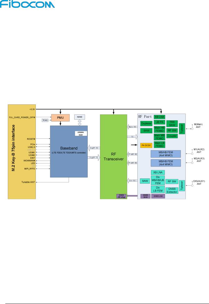
Baseband contains the followings:
GSM/UMTS/LTE FDD controller/Power supply
NAND/internal LPDDR4 RAM
Application interface
RF contains the followings:
RF Transceiver
RF Power/PA
RF Front end
RF Filter
Antenna Connector
Figure 2-2 Hardware Block Diagram
2.6 Antenna Configuration
L860 module support four antennas and the configuration is as below table:
Antenna Connector |
Function Description |
Band configuration |
M |
Main ANT |
All supported bands transmit & receive |
|
|
|
M1 |
MIMO1 ANT |
4x4 MIMO supported bands receive |
|
|
|
M2 |
MIMO2 ANT |
4x4 MIMO supported bands receive |
|
|
|
D/G |
Diversity & GNSS ANT |
All supported bands and GNSS receive |
|
|
|
Reproduction forbidden without Fibocom Wireless Inc. written authorization - All Rights Reserved.
FIBOCOM_L860-GL Hardware User Manual |
Page 16 of 55 |

3 Application Interface
3.1 M.2 Interface
The L860 module applies standard M.2 Key-B interface, with a total of 75 pins.
3.1.1 Pin Map
Figure 3-1 Pin Map
Note:
Pin “Notch” represents the gap of the gold fingers.
Reproduction forbidden without Fibocom Wireless Inc. written authorization - All Rights Reserved.
FIBOCOM_L860-GL Hardware User Manual |
Page 17 of 55 |
 Loading...