


Reproduction forbidden without Fibocom Wireless Inc. written authorization - All Rights Reserved.
FIBOCOM MA510-GL Series Hardware User Manual Page 1 of 66
69100.1000.00.02.61.34_DEMO"
FIBOCOM MA510-GL Series
Hardware User Manual
Version: V1.0.2
Date: 2019-08-19

Reproduction forbidden without Fibocom Wireless Inc. written authorization - All Rights Reserved.
FIBOCOM MA510-GL Series Hardware User Manual Page 2 of 66
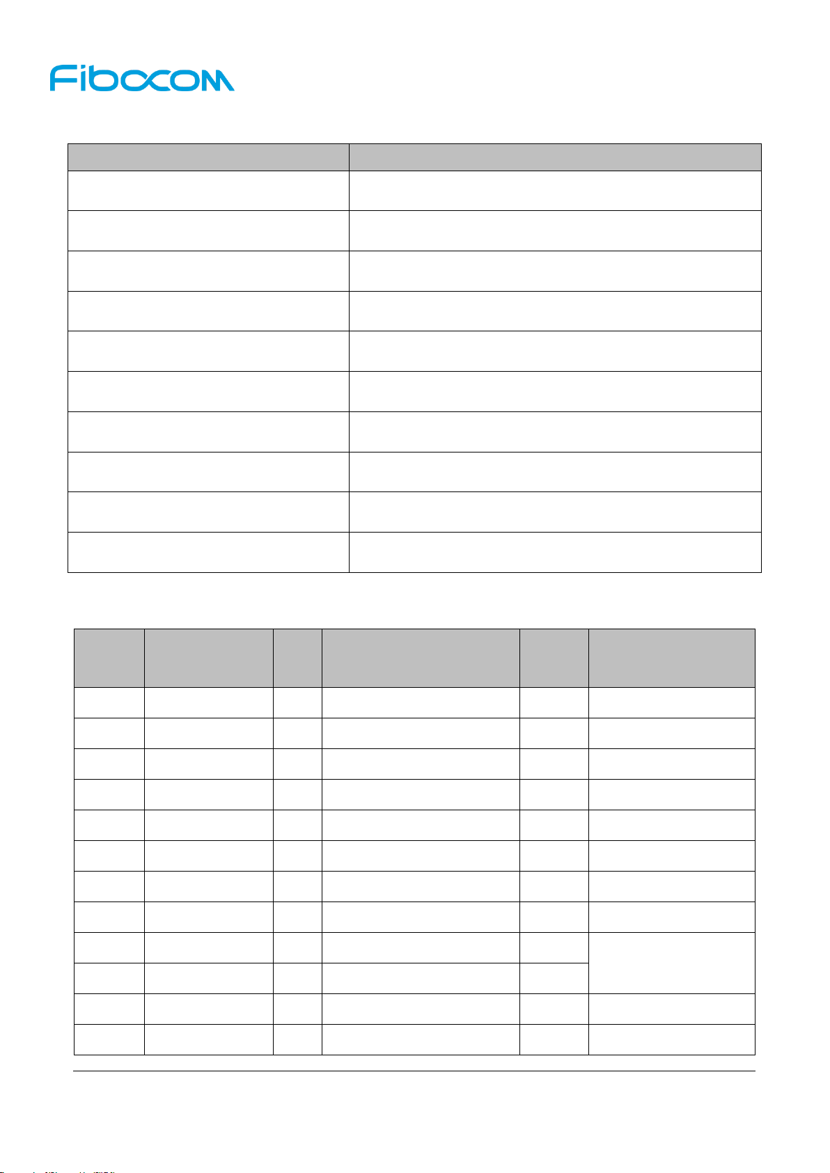
Applicability type
No.
Product model
Power supply voltage range
1
MA510-GL
3.3V~4.5V

Reproduction forbidden without Fibocom Wireless Inc. written authorization - All Rights Reserved.
FIBOCOM MA510-GL Series Hardware User Manual Page 3 of 66
Copyright
Copyright © 2019 Fibocom Wireless Inc. All rights reserved.
Without the prior written permission of the copyright holder, any company or individual is prohibited to
excerpt, copy any part of or the entire document, or transmit the document in any form.
Notice
The document is subject to update from time to time owing to the product version upgrade or other
reasons. Unless otherwise specified, the document only serves as the user guide. All the statements,
information and suggestions contained in the document do not constitute any explicit or implicit
guarantee.
Trademark
The trademark is registered and owned by Fibocom Wireless Inc.

Reproduction forbidden without Fibocom Wireless Inc. written authorization - All Rights Reserved.
FIBOCOM MA510-GL Series Hardware User Manual Page 4 of 66
Versions
Version
Author
Assessor
Approver
Update Date
Description
V1.0.0
Guzhaoqiang
Tumin
Chenguojiang
2019-07-16
Initial version
V1.0.1
Gaoying
Tumin
Chenguojiang
2019-07-30
Update RF parameters
Update some description
V1.0.2
WangNingNing
GaoWenSheng
LiuKe
2019-08-19
Update power consumption
data
Update Power on times
Pin definition
standardization
V1.0.3
WangNingNing
GaoWenSheng
LiuKe
2019-10-11
SIM card hot swap function
update
VBUS voltage range update

Reproduction forbidden without Fibocom Wireless Inc. written authorization - All Rights Reserved.
FIBOCOM MA510-GL Series Hardware User Manual Page 5 of 66
Content
Versions ......................................................................................................................................... 4
Content .......................................................................................................................................... 5
Figure Index .................................................................................................................................. 8
Table Index .................................................................................................................................... 9
1 Introduction........................................................................................................................... 11
1.1 Document Introduction ..........................................................................................................11
1.2 Safety Precautions ................................................................................................................11
2 Product Overview ................................................................................................................. 12
2.1 Product Introduction ............................................................................................................. 12
2.2 Submodel Difference ............................................................................................................ 12
2.3 Product Specification ............................................................................................................ 12
2.4 Functional Diagram .............................................................................................................. 13
2.5 Evaluation Board .................................................................................................................. 14
2.6 CE Statement ....................................................................................................................... 14
3 Pin Description ..................................................................................................................... 16
3.1 Pin Assignment .................................................................................................................... 16
3.2 Pin function ................................................................ .......................................................... 17
4 Operating mode .................................................................................................................... 22
5 Electrical characteristics ..................................................................................................... 23
5.1 Absolute Maximum Ratings .................................................................................................. 23
5.2 Rated voltage ................................ ................................................................ ....................... 23
5.2.1 Power supply design requirements .......................................................................................... 23
5.3 Logic level ............................................................................................................................ 25
5.4 Power consumption .............................................................................................................. 25
6 Functional interface ............................................................................................................. 28
6.1 Control interface ................................................................................................................... 28
6.1.1 Power on................................................................................................................................... 28
6.1.2 Power off ................................................................................................................................... 29
6.1.3 Module reset ............................................................................................................................. 30
6.2 Network status indicate interface .......................................................................................... 31
6.2.1 Interface status description ...................................................................................................... 32
6.3 SIM card interface ................................................................................................................ 32

Reproduction forbidden without Fibocom Wireless Inc. written authorization - All Rights Reserved.
FIBOCOM MA510-GL Series Hardware User Manual Page 6 of 66
6.3.1 SIM pin definition ...................................................................................................................... 32
6.3.2 SIM interface circuit .................................................................................................................. 33
6.3.3 SIM design requirements ......................................................................................................... 35
6.4 USB interface ................................ ................................................................ ....................... 35
6.4.1 USB Pin definition ..................................................................................................................... 35
6.5 UART Interface ..................................................................................................................... 36
6.5.1 UART interface definition.......................................................................................................... 36
6.5.2 UART port application .............................................................................................................. 37
6.6 I2C Interface......................................................................................................................... 38
6.7 ADC interface ....................................................................................................................... 38
6.8 IIS digital audio interface ...................................................................................................... 39
6.8.1 Digital audio interface definition ............................................................................................... 39
6.8.2 Interface application ................................................................................................................. 39
6.9 Antenna tuner interface ........................................................................................................ 39
6.10 Other interfaces .................................................................................................................... 40
7 Low power consumption ..................................................................................................... 41
7.1 Airplane mode ...................................................................................................................... 41
7.2 Sleep mode .......................................................................................................................... 41
7.2.1 USB sleep ................................................................................................................................. 41
7.2.2 UART Application (ATS24 Command ) .................................................................................... 42
7.2.3 UART1_DTR/WAKEUP_IN level control sleep ........................................................................ 42
7.3 Wake Introduction ................................................................................................................ 42
7.3.1 Module is awakened ................................................................................................................. 42
7.3.2 The host is woken up ............................................................................................................... 43
7.4 PSM ..................................................................................................................................... 43
7.5 DRX ..................................................................................................................................... 44
7.6 eDRX ................................................................................................................................... 44
8 RF interface ........................................................................................................................... 45
8.1 Operating band .................................................................................................................... 45
8.2 Output power ........................................................................................................................ 46
8.3 Receive Sensitivity ............................................................................................................... 47
8.4 GNSS Receiver .................................................................................................................... 47
8.5 Antenna design .................................................................................................................... 48
8.5.1 Antenna index ........................................................................................................................... 48

Reproduction forbidden without Fibocom Wireless Inc. written authorization - All Rights Reserved.
FIBOCOM MA510-GL Series Hardware User Manual Page 7 of 66
8.5.2 Antenna reference design ........................................................................................................ 50
9 Reliability .............................................................................................................................. 52
9.1 Environment temperature range ........................................................................................... 52
9.2 Environmental reliability requirements .................................................................................. 52
9.3 ESD characteristics .............................................................................................................. 53
10 Structure specification .................................................................................................. 54
10.1 Product appearance ............................................................................................................. 54
10.2 Structure dimension.............................................................................................................. 54
10.3 PCB Soldering Pad and Stencil Design ................................................................................ 55
10.4 SMT ..................................................................................................................................... 55
10.5 Carrier and storage .............................................................................................................. 55
11 Approval .......................................................................................................................... 56
12 Default information ........................................................................................................ 57
12.1 Serial Port Default Settings .................................................................................................. 57
12.2 Low power mode default setting ........................................................................................... 57
13 Appendix ......................................................................................................................... 57
13.1 GPRS and EGPRS Encoding Scheme ................................................................................. 57
13.2 Terms and acronyms ............................................................................................................ 59
13.3 Related Document................................................................................................................ 61
13.4 Reference Standards ............................................................................................................ 62
13.5 Contact ................................................................................................................................. 62
14 Warnning ......................................................................................................................... 63

Reproduction forbidden without Fibocom Wireless Inc. written authorization - All Rights Reserved.
FIBOCOM MA510-GL Series Hardware User Manual Page 8 of 66
Figure Index
Figure 2-1 Functional Diagram ............................................................................................................ 14
Figure 3-1 Pin Assignment .................................................................................................................. 16
Figure 5-1 Recommend Power Design ............................................................................................ 24
Figure 5-2 Power Limit ........................................................................................................................ 25
Figure 6-1 OC Drive Power on Reference Circuit ............................................................................... 28
Figure 6-2 Button Switch Power on Reference Circuit ....................................................................... 29
Figure 6-3 Power on Timing ................................................................................................................ 29
Figure 6-4 Power off Timing ................................................................................................................ 30
Figure 6-5 OC Driven Reset Reference Circuit .................................................................................. 31
Figure 6-6 Button Reset Reference Circuit ......................................................................................... 31
Figure 6-7 Reset Timing ...................................................................................................................... 31
Figure 6-8 Network Indicate Light Reference Circuits ........................................................................ 32
Figure 6-9 (U)SIM Card Connector without Detection Signal Reference Circuit ................................ 34
Figure 6-10 UART Level Translate Reference 1 ................................................................................. 37
Figure 6-11 UART Level Translate Reference 2 ................................................................................. 38
Figure 6-12 Audio interface Reference Design ................................................................................... 39
Figure 8-1 Main and diversity Antenna Reference Circuit .................................................................. 50
Figure 8-2 Passive GNSS Antenna Reference Circuit........................................................................ 50
Figure 8-3 Active GNSS Antenna Reference Circuit........................................................................... 51
Figure 9-1 Environment Temperature Range...................................................................................... 52
Figure 10-1 Product Appearance ........................................................................................................ 54
Figure 10-2 Structure Dimension (Unit: mm) ...................................................................................... 54

Reproduction forbidden without Fibocom Wireless Inc. written authorization - All Rights Reserved.
FIBOCOM MA510-GL Series Hardware User Manual Page 9 of 66
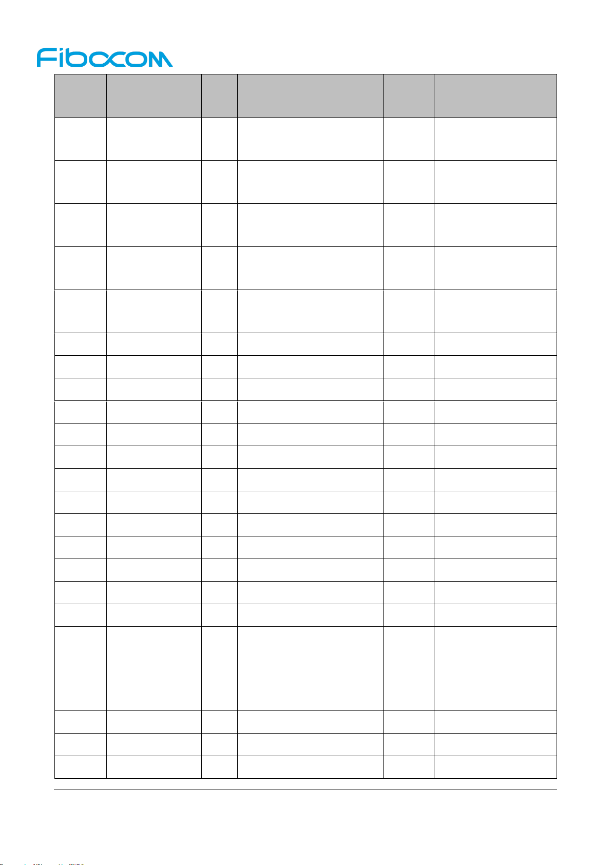
Table Index
Table 2-1 Submodel difference ...................................................................................................................... 12
Table 2-2 Product Specification ...................................................................................................................... 13
Table 3-1 I/O Description Parameters ............................................................................................................ 17
Table 3-2 Pin function description .................................................................................................................. 21
Table 4-1 MA510-GL offers five Operating modes ......................................................................................... 22
Table 5-1 Limit voltage range ......................................................................................................................... 23
Table 5-2 Power Interface .............................................................................................................................. 23
Table 5-3 Capacitance Design Description of External Power Supply Circuit ............................................... 24
Table 5-4 IO Logic Level ................................................................................................................................ 25
Table 5-5 Power Consumption ....................................................................................................................... 27
Table 6-1 Control Signal ................................................................................................................................. 28
Table 6-2 Power off ........................................................................................................................................ 30
Table 6-3 Reset .............................................................................................................................................. 30
Table 6-4 Network Statue Indicate ................................................................................................................. 31
Table 6-5 Network Indicate Light Work Status ............................................................................................... 32
Table 6-6 (U) SIM Card Pin ............................................................................................................................ 33
Table 6-7 (U) SIM Card Hot Plug Function Configuration .............................................................................. 34
Table 6-8 (U) SIM_PRESENCE Effective Level Switched ............................................................................. 35
Table 6-9 USB Pin Definition .......................................................................................................................... 36
Table 6-10 Serial Port 1 .................................................................................................................................. 37
Table 6-11 Serial Port 2 .................................................................................................................................. 37
Table 6-12 Serial Port 3 .................................................................................................................................. 37
Table 6-13 I2C Interface ................................................................................................................................. 38
Table 6-14 ADC Pin Definition ........................................................................................................................ 38
Table 6-15 Digital Audio Interface .................................................................................................................. 39
Table 6-16 Antenna tuned interface ............................................................................................................... 39
Table 6-17 Other Interfaces ............................................................................................................................ 40
Table 7-1 VBUS control sleep state configuration table ................................................................................. 41
Table 7-2 Serial port sleep command configuration example ........................................................................ 42
Table 8-1 RF Interface .................................................................................................................................... 45
Table 8-2 Operating Band .............................................................................................................................. 46
Table 8-3 Output Power.................................................................................................................................. 46

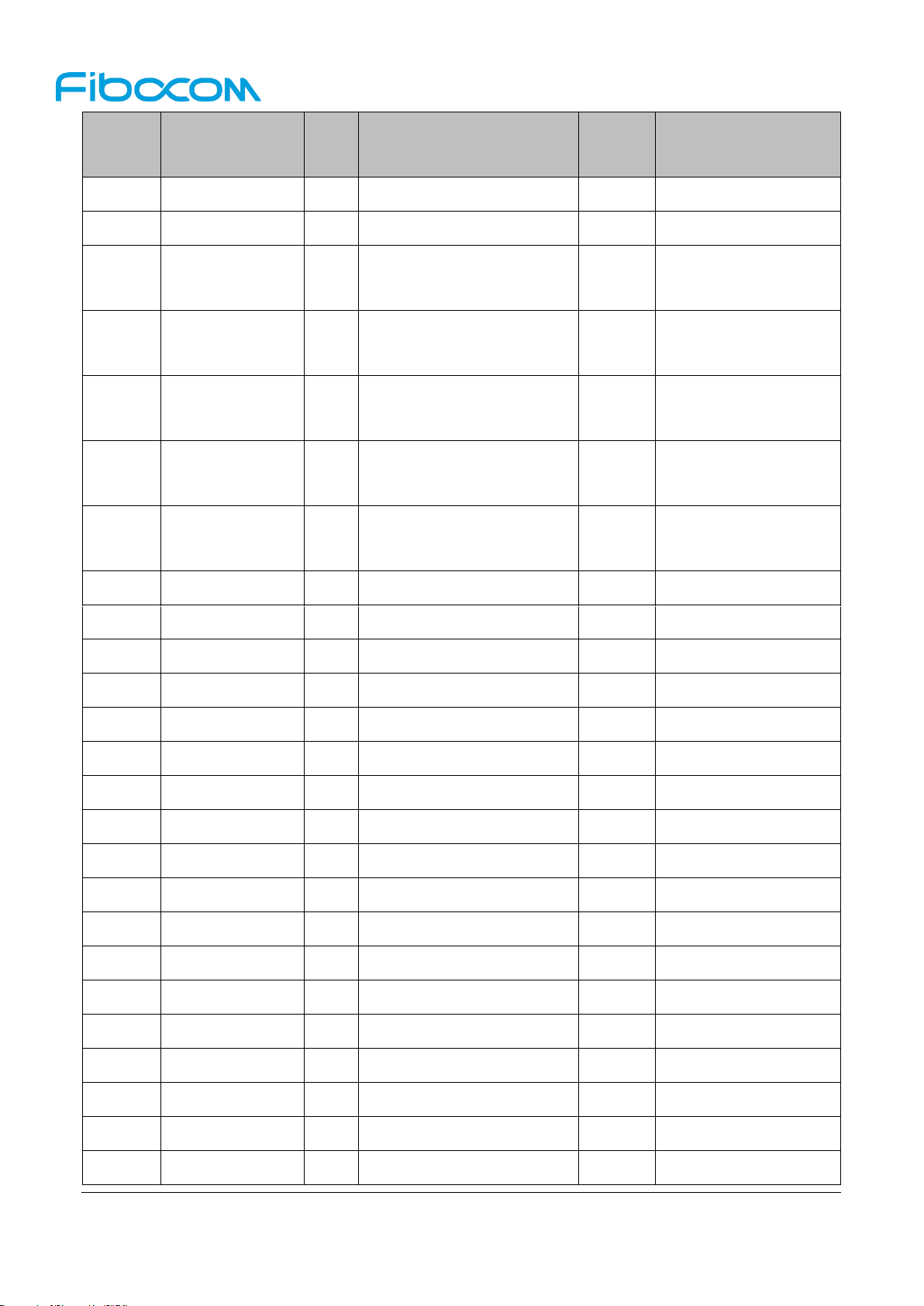
Reproduction forbidden without Fibocom Wireless Inc. written authorization - All Rights Reserved.
FIBOCOM MA510-GL Series Hardware User Manual Page 10 of 66
Table 8-4 Receive Sensitivity ......................................................................................................................... 47
Table 8-5 GNSS Specification ........................................................................................................................ 48
Table 8-6 Main Antenna Requirements .......................................................................................................... 50
Table 9-1 Environment Temperature Range .................................................................................................. 52
Table 9-2 Environmental Reliability Requirements ........................................................................................ 53
Table 9-3 ESD Allowable Discharge Range ................................................................................................... 53
Table 11-1 Approval ........................................................................................................................................ 56
Table 13-1 GPRS Encoding Scheme ............................................................................................................. 57
Table 13-2 Multilevel Multislot Allocation ........................................................................................................ 58
Table 13-3 EGPRS Modulation and Encoding Method ............................................................................... 59
Table 13-4 Terms and Acronyms .................................................................................................................... 61

Reproduction forbidden without Fibocom Wireless Inc. written authorization - All Rights Reserved.
FIBOCOM MA510-GL Series Hardware User Manual Page 11 of 66
1 Introduction
1.1 Document Introduction
This document describes the electrical characteristics, RF performance, structure size, application environment,
etc. of MA510-GL module. With the assistance of the document and other instructions, the developers can
quickly understand the hardware functions of the MA510-GL module and develop products.
1.2 Safety Precautions
By following the safety guidelines below, you can protect the personal safety and help protect the product and
work environment from potential damage. Product manufacturers need to communicate the following safety
instructions to end users. In case of failure to comply with these safety rules, Fibocom Wireless will not be
responsible for the consequences caused by the user’s misuse.
Road safety first! When you drive, do not use the handheld devices even if it has a hand-free
feature. Please stop and call!
Please turn off the mobile device before boarding. The wireless feature of the mobile device is
not allowed on the aircraft to prevent interference with the aircraft communication system.
Ignoring this note may result in flight safety issue or even breaking the law.
When in a hospital or health care facility, please be aware of restrictions on the use of mobile
devices. Radio frequency interference may cause medical equipment to malfunction, so it
may be necessary to turn off the mobile device.
The mobile device does not guarantee that an effective connection can be made under any
circumstances, for example, when there is no prepayment for the mobile device or the (U)SIM
is invalid. When you encounter the above situation in an emergency, remember to use an
emergency call, while keeping your device turned on and in areas where signal is strong.
Your mobile device receives and transmits RF signals when it is powered on. Radio
interference occurs when it is near televisions, radios, computers, or other electronic devices.
Keep the mobile device away from flammable gases. Turn off the mobile device when near
gas stations, oil depots, chemical plants or explosive workplaces. There is a safety hazard in
operating electronic equipment in any potentially explosive environment.
Reproduction forbidden without Fibocom Wireless Inc. written authorization - All Rights Reserved.
FIBOCOM MA510-GL Series Hardware User Manual Page 12 of 66
2 Product Overview
2.1 Product Introduction
MA510-GL series wireless module is a IOT wireless communication module that support multi-mode such
as LTE, GSM (LTE Cat.M1,LTE Cat.NB1/NB2* and EGPRS). It can provide data connection at LTE-FDD,
GPRS and EGPRS network. Supports GNSS (GPS/GLONASS/BeiDou).
2.2 Submodel Difference
Product model
Network type
Power supply voltage range
Note
MA510-GL
CatM+NB2*+GSM
3.3V~4.5V
Tri mode
Table 2-1 Submodel difference
2.3 Product Specification
Specification
Operating frequency
LTE FDD CatM1:
B1/B2/B3/B4/B5/B8/B12/B13/B14/B18/B19/B20/B25/B26/B27/B28/B66/B85
LTE FDD Cat NB1/NB2*:
B1/B2/B3/B4/B5/B8/B12/B13/B18/B19/B20/B25/B26/B28/B66/B71/B85
GSM/GPRS/EGPRS: 850/900/1800/1900
Data transmission
LTE
features
Cat.M1 Rel.14:Max UL 1119kbps,Max DL 589kbps
Cat.NB1 Rel.14:Max UL 66.6kbps,Max DL 34kbps
Cat.NB2* Rel.14:Max UL 150kbps,Max DL 136kbps
GSM
features
GPRS(class33):Max UL 85.6kbps,Max DL 107kbps
EGPRS(class33):Max UL 236.8kbps, Max DL 296kbps
GPS
features
GPS/GLONASS/BDS/Galileo
Power supply
MA510-GL-00
3.3V~4.5V (Recommended 3.8V)
Temperature
Normal:-30°C~+75°C①
Extend:-40°C~+85°C②
Storage:-40°C~+90°C
Physical
Characteristics
Package:LCC 42pin+ LGA 44Pin,86pin in total
Size:22.2 x 20.2 x 2.1 mm
Reproduction forbidden without Fibocom Wireless Inc. written authorization - All Rights Reserved.
FIBOCOM MA510-GL Series Hardware User Manual Page 13 of 66
Weight:1.7±0.2g
Interface
Antenna
Antenna:Main x 1、GNSS x 1
Functional Interface
SIM x 1 1.8V only
USB 2.0 x 1
UART x 3、I2S x 1、I2C x 1、GPIO x 4
System Indicator x 1
ANT_TUNER x 1
ADC x 2
Software
Protocol Stack
Support: PPP/TCP/UDP/SSL/TLS/FTP(S)/HTTP(S) protocol
AT commands
3GPP TS 27.007 and 27.005, and proprietary FIBOCOM AT
Firmware update
FOTA/USB
Voice service
Support
SMS
Support Text and PDU modes;point-to-point MO;MT; cell broadcast
MMS service
Not Support
Table 2-2 Product Specification
Note:
1.
①
Indicates that the module can work normally within this temperature range, and the relevant
performance meets the requirements of the 3GPP standard.
2.
②
Indicates that the module can work normally in this temperature range. The baseband and RF
functions are normal, but individual indicators may exceed the scope of the 3GPP standard. When the
temperature returns to the normal working range of the module, the indicators of the module will still
comply with the 3GPP standard.
3. * indicates that the feature is under development.
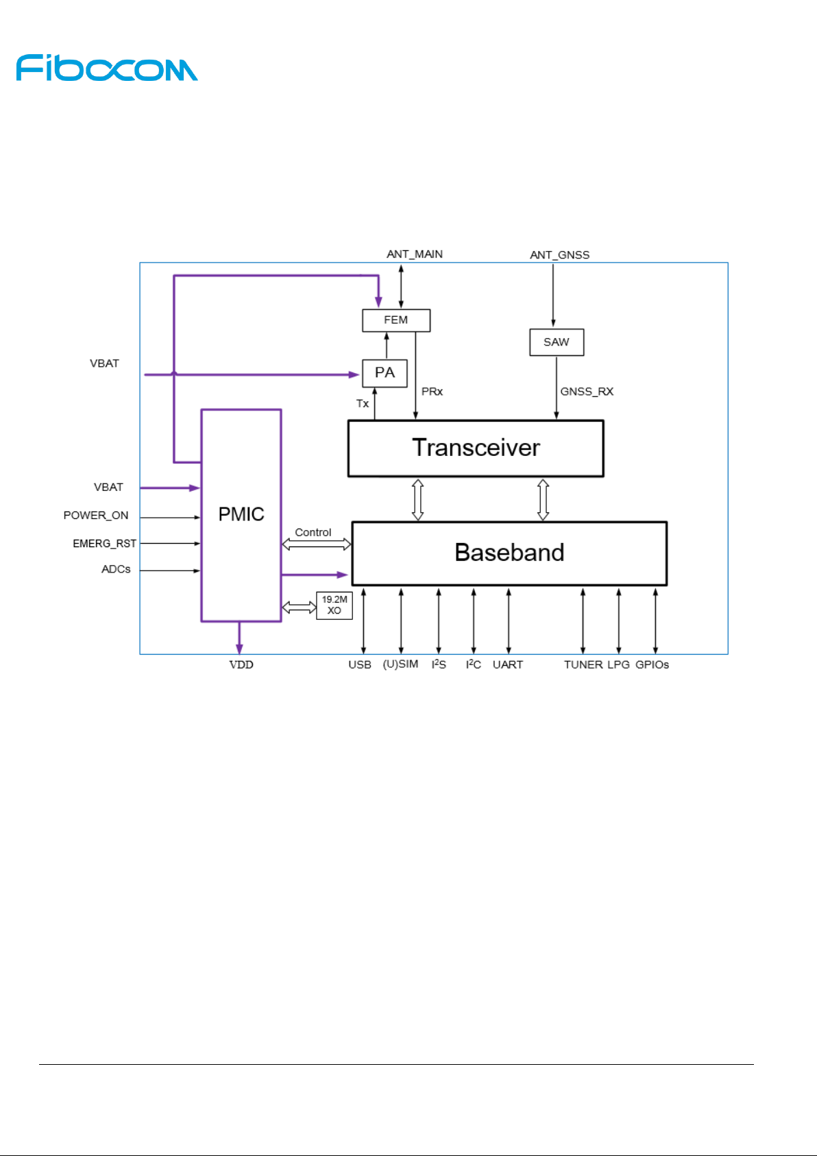
2.4 Functional Diagram
Functional diagram shows the main hardware features of the MA510-GL series module.The Baseband
section contains:
CPU
PMIC
Clock
Function interface
Reproduction forbidden without Fibocom Wireless Inc. written authorization - All Rights Reserved.
FIBOCOM MA510-GL Series Hardware User Manual Page 14 of 66
The RF section contains:
Transceiver
RF PA
RF filter
RF switch
Figure 2-1 Functional Diagram
2.5 Evaluation Board
In order to help test and use the MA510-GL series modules, Fibocom provides evaluation boards. It include
the EVK-GT8230-NL and ADP-MA510-GL-00-00. For details, please refer to the “ADP-MA510-GL Development
Board Instructions” and “GT8230-NL User Manual”.
2.6 CE Statement
► EU Regulatory Conformance
Hereby, We, Manufacturer name declares that the radio equipment type MA510-GL is in compliance with
the Directive 2014/53/EU.
In all cases assessment of the final product must be mass against the Essential requirements of the
Directive 2014/53/EU Articles 3.1(a) and (b), safety and EMC respectively, as well as any relevant Article 3.2
requirements.

Reproduction forbidden without Fibocom Wireless Inc. written authorization - All Rights Reserved.
FIBOCOM MA510-GL Series Hardware User Manual Page 15 of 66
The maximum antenna gain for is 5 dBi and the antenna separation distance is 20cm.
► Declaration of Conformity(should include manufacturer contact info.)
Please added certification standard in your user manual which depended on the test standards your device
performed., If the DoC should be a simplified version, please take below as reference, The full text of the EU
declaration of conformity is available at the following internet address: http//www.fibocom.com.
MA510-GL is in conformity with the relevant Union harmonization legislation: Radio Equipment directive
2014 / 53 / EU with reference to the following standards applied: Health (Article 3.1(a) of Directive 2014/53/EU)
Applied Standard(s): EN 62311 : 2008
Safety (Article 3.1(a) of Directive 2014/53/EU) Applied Standard(s):
EN 60950-1: 2006 + A11: 2009 + A1: 2010 + A12: 2011 + A2: 2013
Electromagnetic compatibility (Article 3.1 (b) of Directive 2014/53/EU) Applied Standard(s):
Draft EN 301 489-1 V2.1.1 /-52 V1.1.0
Radio frequency spectrum usage (Article 3.2 of Directive 2014/53/EU) Applied Standard(s):
EN 301 908-1 V11.1.1
EN 301 908-13 V13.1.1_11.1.4(Draft)
EN 301511 V12.5.1
Reproduction forbidden without Fibocom Wireless Inc. written authorization - All Rights Reserved.
FIBOCOM MA510-GL Series Hardware User Manual Page 16 of 66
3 Pin Description
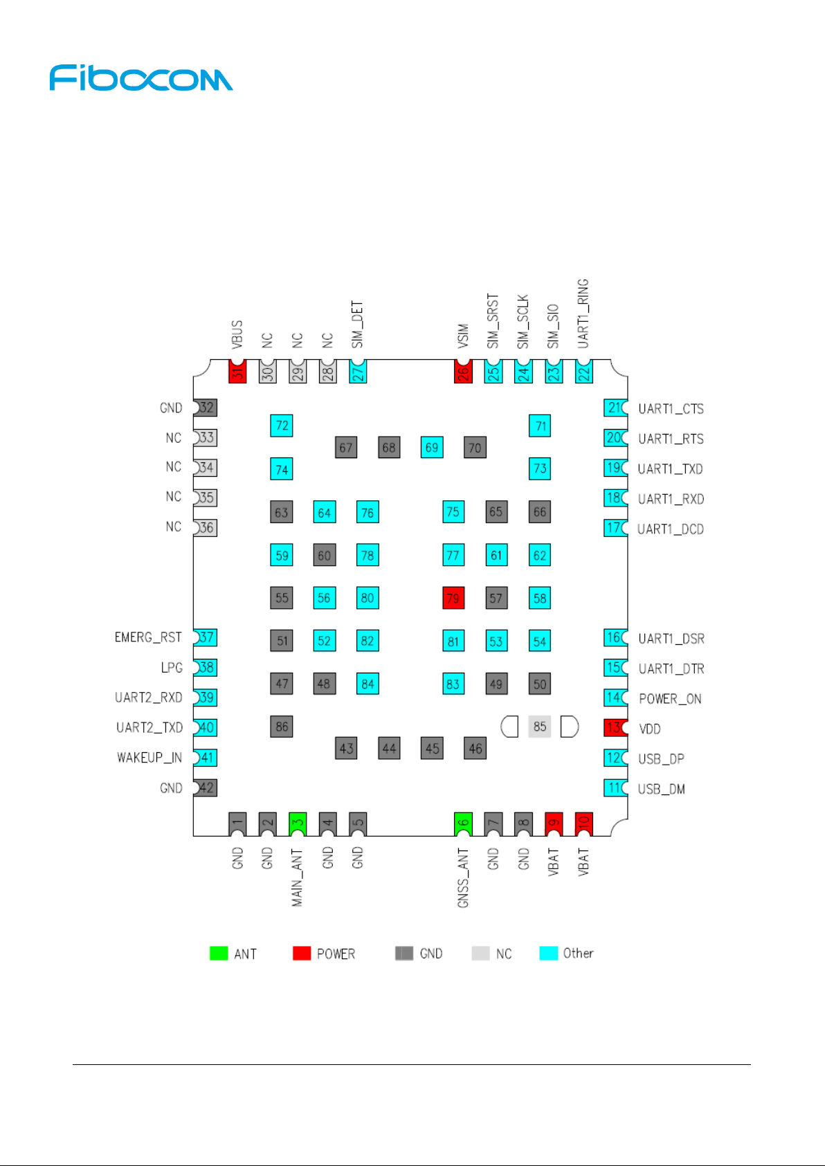
3.1 Pin Assignment
The MA510-GL series module is LCC+LGA package and has 86 pin in total, the pin assignment is
shown as follows:
Figure 3-1 Pin Assignment
Reproduction forbidden without Fibocom Wireless Inc. written authorization - All Rights Reserved.
FIBOCOM MA510-GL Series Hardware User Manual Page 17 of 66
3.2 Pin function
Symbol
Description
I/O
Input/Output
DI
Digital Input
DO
Digital Output
PI
Power Input
PO
Power Output
AI
Analog Input
AO
Analog Output
OD
Open Drain
OC
Open Collector
G
GND
Table 3-1 I/O Description Parameters
The pin function description of MA510-GL series module is shown as table 3-2:
Pin Num
Pin Name
I/O
Description
Power
domain
Note
1
GND
G
GND
2 GND
G
GND
3 MAIN_ANT
I/O
Main antenna
4 GND
G
GND
5 GND
G
GND
6 GNSS_ANT
AI
GNSS antenna
7 GND
G
GND
8 GND
G
GND
9 VBAT
PI
Power supply
3.8V
3.8V is Recommended
voltage
10
VBAT
PI
Power supply
3.8V
11
USB_DM
I/O
USB2.0 difference signal -
12
USB_DP
I/O
USB2.0 difference signal +
Reproduction forbidden without Fibocom Wireless Inc. written authorization - All Rights Reserved.
FIBOCOM MA510-GL Series Hardware User Manual Page 18 of 66
Pin Num
Pin Name
I/O
Description
Power
domain
Note
13
VDD
PO
IO interface power domain
1.8V
80mA drive capability.
Keep it floating if unused
14
POWER_ON
DI
Module power on/off
1.8V
Pull down 0.55-1.7s to
power on
15
UART1_DTR
DI
UART1 module sleep/
wake-up control signal
1.8V
Keep it floating if unused
16
UART1_DSR*
I/O
UART1 data is ready
1.8V
UART1 reserved
function, to be developed
17
UART1_DCD
DO
UART1 module carrier
detection signal output
1.8V
Keep it floating if unused
18
UART1_RXD
DI
UART1 data reception
1.8V
Keep it floating if unused
19
UART1_TXD
DO
UART1 data transmission
1.8V
Keep it floating if unused
20
UART1_RTS
DO
UART1 request to send
1.8V
Keep it floating if unused
21
UART1_CTS
DI
UART1 clear to send
1.8V
Keep it floating if unused
22
UART1_RING
DO
UART1 ring indicator
1.8V
Keep it floating if unused
23
SIM_SIO
I/O
SIM card data signal
1.8V
24
SIM_SCLK
DO
SIM card clock signal
1.8V
25
SIM_SRST
DO
SIM card reset signal
1.8V
26
VSIM
PO
SIM card power supply
1.8V
27
SIM_DET
DI
SIM card detection
1.8V
Keep it floating if unused
28
NC - NC - floating
29
NC - NC - floating
30
NC - NC - floating
31
VBUS
AI
USB power pin
5V
USB plug detect signal,
USB PHY power supply,
Requires more than
100mA drive capability.
32
GND
G
GND
-
-
33
NC - NC - floating
34
NC - NC - floating
Reproduction forbidden without Fibocom Wireless Inc. written authorization - All Rights Reserved.
FIBOCOM MA510-GL Series Hardware User Manual Page 19 of 66
Pin Num
Pin Name
I/O
Description
Power
domain
Note
35
NC - NC - floating
36
NC - NC - floating
37
EMERG_RST
DI
Module reset
1.8V
Pull down 7.5s or more to
reset
38
LPG
DO
Status Indicator light control
1.8V
Need to increase the
drive externally
39
UART2_RXD
DI
UART2 data reception
1.8V
Debug Uart. Keep it
floating if unused
40
UART2_TXD
DO
UART 2 data transmission
1.8V
Debug Uart. Keep it
floating if unused
41
WAKEUP_IN
DI
Module sleep/wake control
signal input
1.8V
Keep it floating if unused
42
GND
G
GND
-
43
GND
G
GND
-
44
GND
G
GND
-
45
GND
G
GND
-
46
GND
G
GND
-
47
GND
G
GND
-
48
GND
G
GND
-
49
GND
G
GND
-
50
GND
G
GND
-
51
GND
G
GND
-
52
I2C_SDA
I/O
I2C data signal
1.8V
Keep it floating if unused
53
GPIO1
I/O
Reserved GPIO
1.8V
Keep it floating if unused
54
GPIO2
I/O
Reserved GPIO
1.8V
Keep it floating if unused
55
GND
G
GND
-
56
I2C_SCL
DO
I2C clock
1.8V
Keep it floating if unused
57
GND
G
GND
-
58
GPIO3
I/O
Reserved GPIO
1.8V
Keep it floating if unused
59
ADC1
AI
Analog digital change
1.8V
Keep it floating if unused

Reproduction forbidden without Fibocom Wireless Inc. written authorization - All Rights Reserved.
FIBOCOM MA510-GL Series Hardware User Manual Page 20 of 66
Pin Num
Pin Name
I/O
Description
Power
domain
Note
60
GND
G
GND
-
61
WAKEUP_OUT
DO
Module wakeup host
1.8V
Keep it floating if unused
62
GPIO_4
I/O
Reserved GPIO
1.8V
Keep it floating if unused
63
GND
G
GND
-
64
AXUADC0
AI
Analog digital change
4.8V
Keep it floating if unused
65
GND
G
GND
-
66
GND
G
GND
-
67
GND
G
GND
-
68
GND
G
GND
-
69
CODEC_EN
DO
External codec enable
1.8V
Keep it floating if unused
70
GND
G
GND
-
71
FORCE_BOOT
DI
Force download
1.8V
connect this pin with
VDD and power on can
force module enter
download mode
72
I2S_DATA1
I/O
I2S data
1.8V
Keep it floating if unused
73
ANT_TUNER1*
DO
Antenna tuner interface
1.8V
In development. Keep it
floating if unused
74
ANT_TUNER1*
DO
Antenna tuner interface
1.8V
In development. Keep it
floating if unused
75
UART2_CTS
DI
UART2 clear to send
1.8V
Debug Uart. Keep it
floating if unused
76
UART2_RTS
DO
UART2 request to send
1.8V
Debug Uart. Keep it
floating if unused
77
UART3_RXD*
DI
UART3 data reception
1.8V
Keep it floating if unused
78
UART3_TXD*
DO
UART3 data transmission
1.8V
Keep it floating if unused
79
NC - NC - floating
80
I2S_MCLK
DO
I2S interface main clock
1.8V
Keep it floating if unused
81
CODEC_INTR
DI
Interrupt signal
1.8V
Can be used as GPIO.
Keep it floating if unused

Reproduction forbidden without Fibocom Wireless Inc. written authorization - All Rights Reserved.
FIBOCOM MA510-GL Series Hardware User Manual Page 21 of 66
Pin Num
Pin Name
I/O
Description
Power
domain
Note
82
I2S_DATA0
I/O
I2S data signal
1.8V
Keep it floating if unused
83
I2S_SCK
DO
I2S serial clock signal
1.8V
Keep it floating if unused
84
I2S_WS
DO
I2S word select signal
1.8V
Keep it floating if unused
85
NC - NC - floating
86
GND
G
GND
-
Table 3-2 Pin function description
Note:The pin function with * is still under development and cannot be used temporarily.

Reproduction forbidden without Fibocom Wireless Inc. written authorization - All Rights Reserved.
FIBOCOM MA510-GL Series Hardware User Manual Page 22 of 66
4 Operating mode
MA510-GL offers five Operating modes as shown in the table below:
Operating
modes
Description
Characteristic
Shutdown
VBAT is powered on and the module is
not started.
Module is off
Standby
The module is fully booted and is
already registered on the network,
ready to communicate at any time. This
is the default working mode after the
module is powered on.
The module is active; All functions are available
normally; Data transmission and reception is
Normal;
Transmission
mode
The module is in data transfer mode.
When it completed, the module returns
to standby or low power mode.
Module successfully registers the network and
performs service transmission.
Sleep
The module is in a light sleep state, the
modules network is connected, and a
paging message can be accepted.
In this mode, the module can be
switched to standby mode or PSM
mode.
The module is put into sleep mode by the AT
command. In the DRX mode, the serial port
communication of the module is normal, and
the serial communication is closed in the PSM
and eDRX modes. In low power mode, the
module is still registered in the network, and
does not need to re-register after waking up.
PSM
The objective of PSM is to make eMTC
device inactive or power-down for most
of the time, to save power and wake up
the device only for a brief time of data
transmission.
PSM achieves power saving by
shutting down everything except PMIC
RTC block, which consumes low power.
Short duration of active communication
Data transmission originated by eMTC devices,
but also possible to engage in DL receive
during the active duration
Table 4-1 MA510-GL offers five Operating mode s

Reproduction forbidden without Fibocom Wireless Inc. written authorization - All Rights Reserved.
FIBOCOM MA510-GL Series Hardware User Manual Page 23 of 66
5 Electrical characteristics
5.1 Absolute Maximum Ratings
The absolute maximum value includes the limit voltage range that the module can withstand and the
maximum current at which the module operates.. Working outside this range may result in damage to the
product.
The limit voltage range of MA510-GL is shown in the following table:
Parameter
Description
MAX
Unit
VBAT
Supply voltage
4.8
V
4.8
V
Average current
0.6 A Instantaneous peak current
2.5 A Sleep current
2mA
Table 5-1 Limit voltage range
5.2 Rated voltage
Table 5-2 show the power interface of MA510-GL series module.
Pin Num
Pin Name
I/O
Description
DC parameter(V)
MIN
TYP
MAX
9,10
VBAT
PI
power input
MA510-GL-00:3.3V
MA510-GL-01:2.65V
3.8V
4.5V
13
VDD
PO
1.8V output(80mA)
1.75
1.8V
1.85
31
VBUS
PI
USB plug detect
3.3
-
5
26
VSIM
PO
SIM card power
supply
-
1.8V
-
Table 5-2 Power Interface
5.2.1 Power supply design requirements
The MA510-GL series module needs to be powered by the VBAT pin. The recommend power design
is shown in Figure 5-1:

Reproduction forbidden without Fibocom Wireless Inc. written authorization - All Rights Reserved.
FIBOCOM MA510-GL Series Hardware User Manual Page 24 of 66
Figure 5-1 Recommend Power Design
Capacitance combination design for power supply is described in the following table:
Recommended
Capacitor
Function
Instruction
220uF
Voltage stabilizing
capacitor
Low ESR capacitance is required to reduce power
fluctuation when the module is working. The
capacitance requirements are as follows:
MA510-GL-00:Not less than 440uF
MA510-GL-01:Not less than 220uF
1uF、100nF
Digital Signal Noise
Eliminate interference from clocks and digital signals
33pF、8pF
900,1800 MHz
Frequency Band
Elimination of Low and Medium Frequency Radio
Frequency Interference
Table 5-3 Capacitance Design Description of External Power Supply Circuit
The power stability can ensure the normal operation of MA510-GL. Customers need specially
attention that the power supply ripple limit for the module is no more than 150mV (the circuit ESR <
50mΩ). When the module is operating in GSM mode (Burst transmit), the maximum operating current can
reach 2.5A, and must ensure that the power voltage is not less than the minimum power supply voltage.
Otherwise, the module may power off or restart. The power limit is shown in Figure 5-2:

Reproduction forbidden without Fibocom Wireless Inc. written authorization - All Rights Reserved.
FIBOCOM MA510-GL Series Hardware User Manual Page 25 of 66
Figure 5-2 Power Limit
5.3 Logic level
The MA510-GL series module supply a 1.8V voltage through the VDD for the use of the internal
digital circuit. The voltage is the logic level of the module and can be used to indicate module Power on/off,
or for external low current (<80mA) circuits such as GPIO pull up. Please leave the signal floating if not
used. The logic level of IO is defined as follows:
Parament
Minimum
Typical
Maximum
Unit
VOH
VDD -0.45
-
VDD
V
VOL 0 -
0.45
V
VIH
0.65 x VDD
-
VDD + 0.3
V
VIL
-0.3
-
0.35 x VDD
V
Table 5-4 IO Logic Level
5.4 Power consumption
The power consumption of MA510-GL series module measured at 3.8V power supply is shown as follow:
Parameter
Mode
Condition
Maximum Current Typ. (mA)
I
off
Power off
Module power off
0.015
I
airplane
Airplane mode
At+cfun=4
0.9
I
psm
Cat.M1
PSM mode
0.0032
Cat.NB
PSM mode
0.0032
I
sleep
Cat.M1
eDRX Cycle Length = 81.92s
0.81
DRX Cycle Length =2.56s
2.61
Cat.NB
eDRX Cycle Length = 91.92s
0.85
DRX Cycle Length =2.56s
1.73

Reproduction forbidden without Fibocom Wireless Inc. written authorization - All Rights Reserved.
FIBOCOM MA510-GL Series Hardware User Manual Page 26 of 66
Parameter
Mode
Condition
Maximum Current Typ. (mA)
I
GPRS-RMS
CS4
GPRS
GSM850@Gamma=3(4UL/1DL)
600
GSM900@Gamma=3(4UL/1DL)
600
DCS1800@Gamma=3(4UL/1DL)
500
PCS1900@Gamma=3(4UL/1DL)
470
I
EGPRS-RMS
MCS9
EGPRS
GSM850@Gamma=6(4UL/1DL)
560
GSM900@Gamma=6(4UL/1DL)
560
DCS1800@Gamma=5(4UL/1DL)
500
PCS1900@Gamma=5(4UL/1DL)
470
I
LTE-RMS
LTE FDD
Cat.M1 B1 @+20dBm
200
Cat.M1 B2 @+20dBm
200
Cat.M1 B3 @+20dBm
200
Cat.M1 B4 @+20dBm
200
Cat.M1 B5 @+20dBm
220
Cat.M1 B8 @+20dBm
220
Cat.M1 B12 @+20dBm
220
Cat.M1 B13 @+20dBm
220
Cat.M1 B14 @+20dBm
220
Cat.M1 B18 @+20dBm
220
Cat.M1 B19 @+20dBm
220
Cat.M1 B20 @+20dBm
220
Cat.M1 B25 @+20dBm
170
Cat.M1 B26 @+20dBm
220
Cat.M1 B27 @+20dBm
220
Cat.M1 B28 @+20dBm
220
Cat.M1 B66 @+20dBm
180

Reproduction forbidden without Fibocom Wireless Inc. written authorization - All Rights Reserved.
FIBOCOM MA510-GL Series Hardware User Manual Page 27 of 66
Parameter
Mode
Condition
Maximum Current Typ. (mA)
Cat.M1 B85 @+20dBm
200
Cat.NB B1 @+20dBm
270
Cat.NB B2 @+20dBm
260
Cat.NB B3 @+20dBm
250
Cat.NB B4 @+20dBm
260
Cat.NB B5 @+20dBm
290
Cat.NB B8 @+20dBm
290
Cat.NB B12 @+20dBm
280
Cat.NB B13 @+20dBm
290
Cat.NB B18 @+20dBm
290
Cat.NB B19 @+20dBm
290
Cat.NB B20 @+20dBm
290
Cat.NB B25 @+20dBm
250
Cat.NB B26 @+20dBm
290
Cat.NB B28 @+20dBm
280
Cat.NB B66 @+20dBm
260
Cat.NB B71 @+20dBm
260
Cat.NB B85 @+20dBm
270
Table 5-5 Power Consumption
Note:Instrument configuration is as follows
Uplink Configuration
Modulation
CH BW
RB allocation
QPSK
10Mhz
1
Modulation
Ntones
Sub-carrier spacing(kHz)
QPSK
1@0
15

Reproduction forbidden without Fibocom Wireless Inc. written authorization - All Rights Reserved.
FIBOCOM MA510-GL Series Hardware User Manual Page 28 of 66
6 Functional interface
6.1 Control interface
Control interfaces are used for module power on/off and reset operations. The pin definitions are as
follows:
Pin Num
Pin name
I/O
Description
Power domain
14
POWER_ON
I
Module power on/off signal control pin
1.8V
37
EMERG_RST
I
Module reset signal control pin
1.8V
Table 6-1 Control Signal
6.1.1 Power on
6.1.1.1 Boot circuit reference design
MA510-GL can be normally powered on by controlling the POWER_ON pin. The module will start to
work after Clients set POWER_ON to low and keep it 550ms~1.7s. It is recommended to use the
open-collector drive circuit for control. The reference circuit is as follows:
Figure 6-1 OC Drive Power on Reference Circuit
Another way to control the POWER_ON pin is to use a push button switch directly. A TVS needs to
be placed near the button for ESD protection. The reference circuit is as follows:

Reproduction forbidden without Fibocom Wireless Inc. written authorization - All Rights Reserved.
FIBOCOM MA510-GL Series Hardware User Manual Page 29 of 66
Figure 6-2 Button Switch Power on Reference Circuit
6.1.1.2 Power on sequence
Figure 6-3 Power on Timing
Note:
Before pulling down the POWER_ON pin, ensure that the VBAT voltage is stable. It is recommended
that the time interval from the power-on of VBAT to the lowering of POWER_ON is not less than 100ms.
The POWER_ON pull-down time should be between 0.55s and 1.7s.
6.1.2 Power off
There are three ways to get the module off:
Power off mode
Power off methods
Applicable scenarios
Hardware power off
Pull down POWER_ON 3.5s~7s
Hardware normal power off
AT power off
AT+ CPWROFF
Software normal power off
Low-voltage shut down
The module will shut down when the
VBAT voltage is too low (below
VBAT_MIN) or when power is lost.
Module is abnormally closed

Reproduction forbidden without Fibocom Wireless Inc. written authorization - All Rights Reserved.
FIBOCOM MA510-GL Series Hardware User Manual Page 30 of 66
Table 6-2 Power off
6.1.2.1 power off sequence
Figure 6-4 Power off Timing
Note:
1. When the module is working normally, do not cut off the power of the module immediately to
avoid damage to the Flash inside the module. It is strongly recommended to turning off the module
with the POWER_ON or AT command before turn off the power supply.
2. When using the AT command to shut down, please make sure that the POWER_ON pin is not
pulled low after the shutdown command is executed, otherwise the module will automatically turn on
again after the module is shut down.
6.1.3 Module reset
The module supports hardware reset and software reset.
Reset mode
Reset method
Hardware reset
Pull down EMERG_RST pin at least 7.5S, then release it
Software reset
Sent AT commands AT+RESET
Table 6-3 Reset
6.1.3.1 Module reset circuit
Clients can control EMERG_RST pin by OC drive circuits or button switch. Corresponding reference
circuit as Figure 6-5 and Figure 6-6:

Reproduction forbidden without Fibocom Wireless Inc. written authorization - All Rights Reserved.
FIBOCOM MA510-GL Series Hardware User Manual Page 31 of 66
Figure 6-5 OC Driven Reset Reference Circuit
Figure 6-6 Button Reset Reference Circuit
The reset timing is shown as follows:
Figure 6-7 Reset Timing
Note:
The reset signal is a sensitive signal. Please keep it away from RF interference and Shielding it with
GND signals, and avoid routing it on the edge of the PCB and the surface (to avoid module reset caused
by ESD).
6.2 Network status indicate interface
MA510-GL series module provides a network status indicate pin, the pin definition is shown as
follows:
PIN Num.
I/O
PIN Name.
Description
Power domain
38 O LPG
Network statue indicator
1.8V
Table 6-4 Network Statue Indicate

Reproduction forbidden without Fibocom Wireless Inc. written authorization - All Rights Reserved.
FIBOCOM MA510-GL Series Hardware User Manual Page 32 of 66
6.2.1 Interface status description
Network status indicate pins are used to drive indicate light and describe module’s network status,
MA510-GL series module network indicate light and network status description are as follows:
Mode
Module Network indicator pin status
Indicator light flash/off
status
Description
1
600ms High/600ms Low
Flash
No SIM card
Request SIM PIN
Registering network
(T<15S)
Register network failed
2
3000ms High /75ms Low
Slow flash
Standby
3
75ms High / 75ms Low
Speed flash
Data link established
4
Low
Always on/off
Voice call
5
High
Always off/on
Sleep
Table 6-5 Network Indicate Light Work Status
MA510-GL series module network indicates light reference design circuits shown as follows:
Figure 6-8 Network Indicate Light Reference Circuits
6.3 (U)SIM card interface
MA510-GL series module has SIM card interface, and only supports 1.8V SIM card.
6.3.1 (U)SIM pin definition
(U)SIM pin definition is shown in the following table:
Pin Num
Pin name
I/O
Description
Power domain
25
SIM_SRST
DO
Reset signal
1.8V
23
SIM_SIO
I/O
SIM DATA
1.8V

Reproduction forbidden without Fibocom Wireless Inc. written authorization - All Rights Reserved.
FIBOCOM MA510-GL Series Hardware User Manual Page 33 of 66
26
VSIM
PO
SIM Power
1.8V
27
SIM_DET
DI
SIM card hot plug detection
1.8V
24
SIM_SCLK
DO
Clock Signal
1.8V
Table 6-6 (U) SIM Card Pin
6.3.2 (U)SIM interface circuit
6.3.2.1 (U)SIM card connector with card detection signal
(U)SIM card connector should be selected for SIM design. It is recommended to use (U)SIM card
connector with hot plug detection function (Fibocom recommend: SIM016-8P-220P).
Figure 6-9 (U) SIM Card Connector (SIM016-8P-220P)
SIM016-8P-220P card connector, DET and POL are short connected when the card is inserted; DET
and POL are disconnected when there is no card. The following is the reference design circuit, (U) SIM
card insert, SIM_DET pin is high level; (U)SIM card pull out, SIM_DET pin is low level.

Reproduction forbidden without Fibocom Wireless Inc. written authorization - All Rights Reserved.
FIBOCOM MA510-GL Series Hardware User Manual Page 34 of 66
Figure 6-10 (U)SIM Card Connector with Detection Signal Reference Circuit
6.3.2.2 (U)SIM card connector without detection signal
Using the card holder without detection signal, the SIM_DET pin remains floating while the hot-swap
function is turned off by the AT command. Reference circuit as shown below:
Figure 6-11 (U) SIM Card Connector without Detection Signal Reference Circuit
6.3.3 (U)SIM hot plug
MA510-GL series module support (U)SIM hot plug function, it determines the insertion and removal
of (U)SIM card by detect the SIM_ DET pin state.
The card hot plug function can be configured by the “AT+MSMPD” command, and the AT commands
are shown in the following table:
AT command
(U)SIM card hot plug detection
Function description
AT+MSMPD=1
Enabled
(U)SIM card hot plug detection is enabled by default.
AT+MSMPD=0
Disabled
(U)SIM card hot plug detection function is disabled.
The module read the (U)SIM card when module
power on, and does not detect the SIM_DET state.
Table 6-7 (U) SIM Card Hot Plug Function Configuration

Reproduction forbidden without Fibocom Wireless Inc. written authorization - All Rights Reserved.
FIBOCOM MA510-GL Series Hardware User Manual Page 35 of 66
After the hot plug detection function of the (U)SIM card is enabled, if SIM_DET is in high level, the
module will detect the (U)SIM card insertion and execute card initialization program. After reading the
(U)SIM card information, the module will register network. When the SIM_DET is in low level, the module
detects (U)SIM card removed, and it will not read the (U)SIM card.
Note:
The SIM_DET pin active high by default, and can be switched to active low by AT command.
AT command
Function description
AT+GTSET=” SIMPHASE”,1
Default, high level detect
AT+GTSET=” SIMPHASE”,0
Low level detect
Table 6-8 (U) SIM_PRESENCE Effective Level Switched
6.3.4 (U)SIM design requirements
SIM card circuit design shall meet EMC standards and ESD requirements, and at the same time,
shall improve anti-interference ability to ensure that the SIM card can work stably. The design needs to
strictly observe the following rules:
SIM card connector is placed as close to the module as possible, away from the RF antenna, DCDC
power, clock signal lines and other strong interference sources;
Adopt the SIM card connector with metal shield shell to improve anti-interference ability;
The length of cable from the module to the SIM card connector shall not exceed 100mm. Longer
cable reduces signal quality.
SIM_SCLK and SIM_SIO signals are ground isolated to avoid mutual interference. If it is difficult to
do so, SIM signal needs to be ground protected as a set;
The filter capacitor and ESD device of SIM card signal cable should place close to the SIM card
connector.
Please select equivalent capacitor is less than 22pF for ESD device.
SIM_SIO should pull up to VSIM with a 10K resistor.
6.4 USB interface
MA510-GL series module supports USB2.0. For USB bus timing and electric features, please refer
to“Universal Serial Bus Specification 2.0”.
6.4.1 USB Pin definition
Pin Num.
Pin name
I/O
Description
11
USB_DM
IO
USB differential data bus D-
12
USB_DP
IO
USB differential data bus D+

Reproduction forbidden without Fibocom Wireless Inc. written authorization - All Rights Reserved.
FIBOCOM MA510-GL Series Hardware User Manual Page 36 of 66
Pin Num.
Pin name
I/O
Description
31
VBUS
AI
USB plug detect, USB PHY power
supply, Requires more than 100mA
drive capability.
Table 6-9 USB Pin Definition
Note:
It is recommended to reserve USB port for download software.In order to ensure USB performance,
when design USB interface circuit, following rules must be followed:
USB_DM and USB_DP signal cable’s control differential impedance is 90 ohm
USB signal cable must not under crystal, oscillator, magnetic device, RF signal. It is
recommended to take the inner differential cable and the cable shall be grounded at all directions;
The model selection for ESD protection of USB data cable requires special attention, and the
parasitic capacitance must not exceed 1pF;
ESD protector of USB should be placed close to the USB interface.
VBUS be used as USB plug detect and USB PHY power supply, its driven strength should more
than 100mA.
6.5 UART Interface
6.5.1 UART interface definition
MA510-GL series module has three serial ports: serial port 1, serial port 2 and serial port 3. The
serial ports 1 supports 4800bps,9600bps,19200bps,38400bps,57600bps,115200bps,230400bps,
460800bps and 921600bps baud rate. The default baud rate is 115200bps. The serial ports 1 is used for
data transmission and AT command transmission. The pin definition of serial port 1 is shown as follows:
Pin Num
Pin Name
I/O
Description
Note
18
UART1_RXD
DI
UART1 data reception
1.8V
19
UART1_TXD
DO
UART1 data transmission
1.8V
20
UART1_RTS
DO
UART1 request to send
1.8V
21
UART1_CTS
DI
UART1 clear to send
1.8V
22
UART1_RING
DO
UART1 Ring indicator
1.8V
15
UART1_DTR
DI
UART1 module sleep/ wake-up
control signal
1.8V
16
UART1_DSR
I/O
UART1 Reserved, to be developed
1.8V
17
UART1_DCD
DO
UART1 module carrier detection
signal output
1.8V

Reproduction forbidden without Fibocom Wireless Inc. written authorization - All Rights Reserved.
FIBOCOM MA510-GL Series Hardware User Manual Page 37 of 66
Table 6-10 Serial Port 1
The port 2 is debug serial port by default, can used for module debug but cannot for AT function. The
pin definition of serial port 2 is show as follows:
Pin Num
Pin Name
I/O
Description
Note
39
UART2_RXD
DI
UART2 data reception
1.8V
40
UART2_TXD
DO
UART2 data transmission
1.8V
75
UART2_CTS
DI
UART2 clear to send
1.8V
76
UART2_RTS
DO
UART2 request to send
1.8V
Table 6-11 Serial Port 2
The function of serial port 3 is developing and not for AT function.
Pin Num
Pin Name
I/O
Description
Note
77
UART3_RXD
DI
UART3 data reception
1.8V
78
UART3_TXD
DO
UART3 data transmission
1.8V
Table 6-12 Serial Port 3
6.5.2 UART port application
The serial port level of MA510-GL series module is 1.8V, if the level of the client host system is 3.3V
or other, level translator is needed between the module and the host. The reference design circuit of level
translator is shown as follows:
Figure 6-12 UART Level Translate Reference 1
Another level shifting circuit is shown below. The input and output circuit design of the dotted line
below can refer to the solid line part, but pay attention to the connection direction.

Reproduction forbidden without Fibocom Wireless Inc. written authorization - All Rights Reserved.
FIBOCOM MA510-GL Series Hardware User Manual Page 38 of 66
Figure 6-13 UART Level Translate Reference 2
Note:
Transistor level conversion circuit is not suitable for applications of baud rates above 460Kbps.
6.6 I2C Interface
The MA510-GL series modules provide an I2C interface that can be used to control external codec
and other slave devices. External pull-up resistors must be added during use.
PIN Num.
PIN Name
I/O
Description
Note
52
I2C_SDA
I/O
I2C data signal
1.8V Need External pull-up
56
I2C_SCL
DO
I2C clock signal
1.8V Need External pull-up
Table 6-13 I2C Interface
6.7 ADC interface
MA510-GL series module support two channels ADC interface, can used for voltage detect and
other external circuit.
Pin Num.
PIN Name
I/O
Description
Note
59
ADC1
AI
Analog ADC voltage input,
detect voltage range: 0~1.8V
Accuracy is ±15mV
64
ADC0
AI
Analog ADC voltage input,
detect voltage range:0~VBAT
Accuracy is ±120mV
Table 6-14 ADC Pin Definition
Note:
It is recommended to ground shielding when routed to increase voltage detect accuracy and input

Reproduction forbidden without Fibocom Wireless Inc. written authorization - All Rights Reserved.
FIBOCOM MA510-GL Series Hardware User Manual Page 39 of 66
voltage must not exceed voltage range.
6.8 IIS digital audio interface
The MA510-GL provides a digital voice interface (I2S) that uses the domestic mainstream European
E1 standard to enable communication with digital audio devices such as external CODECs.
6.8.1 Digital audio interface definition
PIN Num.
PIN Name
I/O
PIN Num.
Note
82
I2S_DATA0
I/O
I2S data signal0
1.8V
83
I2S_SCK
DO
I2S serial clock signal
1.8V
84
I2S_WS
DO
I2S word select signal
1.8V
72
I2S_DATA1
I/O
I2S data signal1
1.8V
80
I2S_MCLK
DO
I2S main clock signal
1.8V
Table 6-15 Digital Audio Interface
6.8.2 Interface application
Figure 6-14 Audio interface Reference Design
6.9 Antenna tuner interface
The MA510-GL series modules can use ANT_TUNER1 and ANT_TUNER2 as antenna tuning
interfaces:
PIN Num.
PIN Name
I/O
Description
Note
73
ANT_TUNER1
DO
GRFC function reserved
can be used as normal GPIO
74
ANT_TUNER1
DO
GRFC function reserved
can be used as normal GPIO
Table 6-16 Antenna tuned interface

Reproduction forbidden without Fibocom Wireless Inc. written authorization - All Rights Reserved.
FIBOCOM MA510-GL Series Hardware User Manual Page 40 of 66
6.10 Other interfaces
MA510-GL series module also provide interface such as GPIO, WAKEUP_IN, WAKEUP_OUT to
clients.
PIN
Num.
PIN Name
I/O
Description
41
WAKE_UP
DI
Host wakeup module
61
WAKEUP_OUT
DO
Module wakeup host
71
FORCE_USB_B
OOT
DI
Force download
connect this pin with VDD_IO and
Power on can force module enter
download mode
69
CODEC_EN
DO
External codec enable
control
81
CODEC_INTR
DI
Interrupt signal
can be used as normal GPIO
53
GPIO1
I/O
Reserved GPIO
54
GPIO2
I/O
Reserved GPIO
58
GPIO3
I/O
Reserved GPIO
62
GPIO4
I/O
Reserved GPIO
Table 6-17 Other Interfaces

Reproduction forbidden without Fibocom Wireless Inc. written authorization - All Rights Reserved.
FIBOCOM MA510-GL Series Hardware User Manual Page 41 of 66
7 Low power consumption
7.1 Airplane mode
When MA510-GL module enters airplane mode, RF function are closed and all commands related to
RF cannot be used. The way to control module to enter airplane mode is shown as follows:
Send AT+CFUN=<fun> commands, paraments <fun> can be 0,1 or 4;
0:minimum function mode; close RF function and (U)SIM card function;
1:all function mode(by default);
4:close RF function(airplane mode);
7.2 Sleep mode
Sleep mode is also called low power mode. In order to minimize battery loss, when the module is
idle, it enters sleep mode to save power. When the module is in sleep mode, if there is a wakeup source,
the corresponding module should also be woken up to normal operation mode.
The sleep of the MA510-GL can be divided into two parts, one is USB and the other is UART. The
module goes to sleep after the USB and UART are simultaneously sleeping.
7.2.1 USB sleep
USB sleep is mainly divided into two sleep modes:
a. The Vbus signal of the USB bus controls sleep;
b. USB suspend;
7.2.1.1 VBUS control sleep
If the product does not support USB suspend, but VUBS detection is supported. It can be judged
whether the USB is put into hibernation by detecting the VBUS pin level. The specific judgment criteria
are as follows:
Vbus level status
Module status
Note
High
Active
low
Sleep
Table 7-1 VBUS control sleep state configuration table
7.2.1.2 USB suspend
If the host supports USB Suspend/Resume, by setting the level and control of the USB in the Linux
system to auto, the module and the host are left for about 2 seconds, and the module automatically

Reproduction forbidden without Fibocom Wireless Inc. written authorization - All Rights Reserved.
FIBOCOM MA510-GL Series Hardware User Manual Page 42 of 66
enters the Suspend state.
7.2.2 UART Application (ATS24 Command )
The sleep mode controlled by ATS24 command is light sleep. When the RXD of the UART has a
message, the system will wake up. The power consumption in sleep mode by this way is slightly higher
than using the UART1_DTR control mode.
The ATS24 automatically sleeps down. It does not strictly sleep in time. It is attempted to go to sleep
after timeout. If the system does not support hibernation after timeout, it will automatically re-time.
7.2.3 UART1_DTR/WAKEUP_IN level control sleep
When the host and the MA510-GL module are connected through the serial port, you can set the
UART1_DTR /WAKEUP_IN to control the serial port sleep function by sending an AT command. Client refer to
the serial port sleep command configuration example for details.
The serial port sleep configuration command is shown in the following table:
No
Command configuration
Explanation
1
AT+GTLPMMODE=0
ATS24=5
Choose to sleep through the ATS24 command.
The serial port will go to sleep in 5S if there are no data
interaction.
2
AT+GTLPMMODE=2,0
Select to control sleep through UART1_DTR. Pull the pin
high then the serial port sleep.
3
AT+GTLPMMODE=2,1
Select to control sleep through UART1_DTR. Pull the pin
low then the serial port sleep.
4
AT+GTLPMMODE=1,0
Select to control sleep through WAKEUP_IN. Pull the pin
high then the serial port sleep.
5
AT+GTLPMMODE=1,1
Select to control sleep through WAKEUP_IN. Pull the pin
low then the serial port sleep.
Table 7-2 Serial port sleep command configuration example
7.3 Wake Introduction
7.3.1 Module is awakened
When the module is in the sleep state, it can be woken up in the following ways.
7.3.1.1 USB wake up
If the module is USB_VBUS control to sleep, the USB will be woken up when USB_VBUS is pulled
high;

Reproduction forbidden without Fibocom Wireless Inc. written authorization - All Rights Reserved.
FIBOCOM MA510-GL Series Hardware User Manual Page 43 of 66
If the module support USB suspend, any active (non-idle signal) on the bus can wake up the device
and exit the low power mode.
7.3.1.2 UART wake up
If the module enter to sleep through DTR/WAKEUP_IN, controlling DTR/WAKEUP_IN can wake up
the serial port;
If the module uses ATS24 to automatically sleep, when the serial port sends data, the serial port will
be awakened and will automatically go to sleep when timeout.
7.3.2 The host is woken up
When the host is in sleep state, the module needs to output the pulse waveform through the
UART1_RING/WAKEUP_OUT pin to wake up the host in order to detect the module's phone, SMS, data
service and URC report. At this point, the host must configure the connection
UART1_RING/WAKEUP_OUT pin as the wake-up source.
7.4 PSM
Power Saving Mode (PSM) is a feature for eMTC devices and applications that have the following
requirements:
• Infrequently active
• Short duration of active communication
• Data transmission originated by eMTC devices, but also possible to engage in DL receive during
the active duration
• Power constraint, battery-operated
• Long battery life
The objective of PSM is to make eMTC device inactive or power-down for most of the time, to save
power and wake up the device only for a brief time of data transmission.
PSM achieves power saving by shutting down everything except PMIC RTC block, which consumes
low power.
The MA510-GL module can enable the PSM function with AT command (AT+CPSMS=1) and do
as follows If you want to exit PSM.
The method of wake up the module from the PSM state as follows:
1. Pull down the POWER_ON pin and keep it 0.55-1.7s;
2. Wait for the timer (T3412) expires, the module will automatically wake up.
Note:
For more information about AT command please refer to document《FIBOCOM AT Commands User

Reproduction forbidden without Fibocom Wireless Inc. written authorization - All Rights Reserved.
FIBOCOM MA510-GL Series Hardware User Manual Page 44 of 66
Manual》
7.5 DRX
The MA510-GL supports the DRX mode. The module will automatically enter the DRX mode with
lower power consumption if the module does not apply for PSM and eDRX, and there is no data service
interaction. In this mode, the bottom current of the module is reduced to about 700uA, and the average
power consumption is 1.7mA.
7.6 eDRX
The MA510-GL has access to the eDRX low-power mode, which significantly reduces power
consumption to less than 700uA. When the module needs to enter eDRX, it will send the request in the
request message. The network configures the request value of the module in the response message,
and the module enters the eDRX mode. In this mode, the internal part of the module is powered off, and
the module has been registered on the network, it can quickly enter the standby state after waking up.
To enter eDRX, you need to send the following AT command:
AT+CEDRXS=1 or AT+CEDRXS=2,5,”0011”
Note:
The module saves the eDRX configuration. Once eDRX is successfully set, you can still enter eDRX
mode after restarting the module unless you have sent an exit command. The user can enter the eDRX
mode by sending an AT command and request the period of the network side eDRX. When the eDRX
period sent by the network side is greater than 81.92s, the module enters the deep sleep mode,
otherwise it is the light sleep mode. 0011 indicates that the eDRX period requested by the user to the
network is 40.96s, and the user can set it according to the protocol.
You can use the AT+CEDRXRDP command to query the period value of the eDRX and the PTW
window time delivered by the network.
To exit eDRX, you need to send the following AT command:
AT+CEDRXS=0
Note:
The module will save the eDRX configuration. Once the command is successfully sent to exit the
eDRX mode, if the command to enter the eDRX is not resent, the module will not enter the eDRX mode,
and the restart will be the same.

Reproduction forbidden without Fibocom Wireless Inc. written authorization - All Rights Reserved.
FIBOCOM MA510-GL Series Hardware User Manual Page 45 of 66
8 RF interface
MA510-GL series module has MAIN_ANT and GNSS_ANT two antenna interfaces, its pin definition
is shown as table 8-1:
Pin Name
I/O
Pin Num.
Description
MAIN_ANT
I/O 3 Main antenna
GNSS_ANT
I 6 GNSS antenna
Table 8-1 RF Interface
8.1 Operating band
Network mode
Band
Receive
Transmit
Unit
GSM
GSM850
869~894
824~849
MHz
EGSM900
925~960
880~915
MHz
DCS1800
1805~1880
1710~1785
MHz
PCS1900
1930~1990
1850~1910
MHz
FDD-LTE
Band1
2110~2170
1920~1980
MHz
Band2
1930~1990
1850~1910
MHz
Band3
1805~1880
1710~1785
MHz
Band4
2110~2155
1710~1755
MHz
Band5
869~894
824~849
MHz
Band8
925~955
880~910
MHz
Band12
728~746
699~716
MHz
Band13
746~756
777~787
MHz
Band14(only CatM1)
758~768
788~798
MHz
Band18
860~875
815~830
MHz
Band19
875~890
830~845
MHz
Band20
791~821
832~862
MHz
Band25
1930~1995
1850~1915
MHz
Band26
859~894
814~849
MHz
Band27(only CatM1)
852~869
807~824
MHz
Band28
758~803
703~748
MHz
Band66
2110~2180
1710~1780
MHz
Band71(only NB)
617~652
663~698
MHz
Band85
728~746
698~716
MHz

Reproduction forbidden without Fibocom Wireless Inc. written authorization - All Rights Reserved.
FIBOCOM MA510-GL Series Hardware User Manual Page 46 of 66
Table 8-2 Operating Band
8.2 Output power
The RF output power of MA510-GL show as follows:
Network mode
Band
Max
Min
GPRS
GSM850
32.5dBm±1dB
5dBm±3.5dB
EGSM900
32.5dBm±1dB
5dBm±3.5dB
DCS1800
29.5dBm±1dB
0dBm±3.5dB
PCS1900
29.5dBm±1dB
0dBm±3.5dB
EGPRS
GSM850
26dBm±1dB
5dBm±3.5dB
EGSM900
26dBm±1dB
5dBm±3.5dB
DCS1800
25dBm±1dB
0dBm±3.5dB
PCS1900
25dBm±1dB
0dBm±3.5dB
FDD-LTE
Band1
20dBm±1dB
<-44dBm
Band2
20dBm±1dB
<-44dBm
Band3
20dBm±1dB
<-44dBm
Band4
20dBm±1dB
<-44dBm
Band5
20dBm±1dB
<-44dBm
Band8
20dBm±1dB
<-44dBm
Band12
20dBm±1dB
<-44dBm
Band13
20dBm±1dB
<-44dBm
Band14(only CatM1)
20dBm±1dB
<-44dBm
Band18
20dBm±1dB
<-44dBm
Band19
20dBm±1dB
<-44dBm
Band20
20dBm±1dB
<-44dBm
Band25
20dBm±1dB
<-44dBm
Band26
20dBm±1dB
<-44dBm
Band27(only CatM1)
20dBm±1dB
<-44dBm
Band28
20dBm±1dB
<-44dBm
Band66
20dBm±1dB
<-44dBm
Band71(only NB)
20dBm±1dB
<-44dBm
Band85
20dBm±1dB
<-44dBm
Table 8-3 Output Power

Reproduction forbidden without Fibocom Wireless Inc. written authorization - All Rights Reserved.
FIBOCOM MA510-GL Series Hardware User Manual Page 47 of 66
8.3 Receive Sensitivity
Network mode
Band
Cat.M1
Sensitive/3GPP(dBm)
Cat.NB1
Sensitive/3GPP(dBm)
FDD-LTE
Band1
-106.6/-102.3
-118.2/-107.5
Band2
-106.9/-100.3
-118.2/-107.5
Band3
-104.5/-99.3
-119.2/-107.5
Band4
-105/-102.3
-118.2/-107.5
Band5
-104.5/100.8
-118.2 /-107.5
Band8
-105.2/-99.8
-118/-107.5
Band12
-104/-99.3
-118.2/-107.5
Band13
-103.2/-99.3
-118.2/-107.5
Band14(only CatM1)
-103.3/-99.3
nonsupport
Band18
-106/-102.3
-118.2/-107.5
Band19
-103.7/-102.3
-117.2/-107.5
Band20
-105.2/-99.8
-118.2/-107.5
Band25
-107.3/-99.3
-118.2/-107.5
Band26
-104.6/-100.3
-117.2/-107.5
Band27(only CatM1)
-106.4/-100.8
nonsupport
Band28
-105.6/-100.8
-118.2/-107.5
Band66
-106.2/-101.7
-118.2/-107.5
Band71(only NB)
nonsupport
-117.2/-107.5
Band85
-106/-99.2
-118.2/-107.5
Table 8-4 Receive Sensitivity
8.4 GNSS Receiver
MA510-GL series module support GNSS/GLONASS and GPS/BeiDou function and adopts
Qualcomm Gen9 technology.
Description
Condition
Typ.
Note
Power Consumption
(AT+CFUN=0)
GNSS fixing
75mA
USB plug in
GNSS tracking
73mA
USB plug in
Standby
31
USB plug in
TTFF
GNSS
Cold start (XTRA enable)
45s

Reproduction forbidden without Fibocom Wireless Inc. written authorization - All Rights Reserved.
FIBOCOM MA510-GL Series Hardware User Manual Page 48 of 66
Description
Condition
Typ.
Note
Warm start(XTRA enable)
40s
Hot Start (XTRA enable)
5s
Sensitivity
Acquisition
Open Sky
-144dbm
tracking
Open Sky
-160dbm
CN0
GNSS Signal@-130dBm
37dB-HZ
Positional
Accuracy
CEP
GNSS Signal @-130dBm
4m
Table 8-5 GNSS Specification
8.5 Antenna design
8.5.1 Antenna index
1) Antenna efficiency
Antenna efficiency is the ratio of antenna input power to radiated power. Due to the antenna return
loss, material loss, and coupling loss, the radiated power is always lower than the input power.
Recommend> 40% (-4dB).
2) S11 or VSWR
S11 shows that the matching degree of the antenna’s 50 ohm impedance, to a certain extent, affects
the antenna efficiency. VSWR test methods can be used to measure this parameter. Recommend S11
<-10dB.
3) Polarization
Polarization is the rotation direction of the electric field in the maximum radiation direction of the
antenna.
It is recommended to use linear polarization.
4) Radiation pattern
Radiation pattern refers to the antenna’s electromagnetic field strength in the far field in all directions.
Half-wave dipole antenna is the most suitable terminal antenna. For built-in antenna, PIFA antennas or
IFA antennas are recommended:
Antenna area: 6mm high*10mm wide*100mm long.
Antenna radiation direction: Omni_directional(all direction).
5) Gain and directivity
Antenna directivity refers to the electromagnetic field strength of electromagnetic wave in all
directions. Gain is a collection of antenna benefits and antenna directivity.

Reproduction forbidden without Fibocom Wireless Inc. written authorization - All Rights Reserved.
FIBOCOM MA510-GL Series Hardware User Manual Page 49 of 66
Recommended antenna gain ≤2.5dBi.
6) Interference
In addition to the antenna performance, other interferences on the PCB also affect the performance
of the module. In order to ensure the high performance of the module, interference must be controlled.
Suggestions: For example, LCD, CPU, FPC cable, audio circuit, power supply should be away from the
antenna as far as possible, and make the appropriate isolation and shielding, or filtering on the path.
7) Antenna index requirements
MA510-GL series module main antenna requirements
Frequency range
It must use the most suitable antenna to adapt to the relevant frequency band
Bandwidth
(
GSM/EDGE)
GSM850: 70 MHz
GSM900: 80 MHz
GSM1800(DCS): 170 MHz
GSM1900(DCS): 140 MHz
Bandwidth (LTE)
LTE band 1(2100): 250 MHz
LTE band 2(1900): 140 MHz
LTE Band 3(1800): 170 MHz
LTE Band 4(2100): 445 MHz
LTE Band 5(850): 70 MHz
LTE Band 8(900): 80 MHz
LTE Band 12(700): 47 MHz
LTE Band 13(700): 41 MHz
LTE Band 14(700): 40 MHz
LTE Band 18(700): 60 MHz
LTE Band 19(700): 60 MHz
LTE Band 20(700): 71 MHz
LTE Band 25(700): 145 MHz
LTE Band 26(700): 80 MHz
LTE Band 27(700): 62 MHz
LTE Band 28(700):100 MHz
LTE Band 66(2100):470 MHz
LTE band 71(2600): 81 MHz
LTE band 85(2300):48 MHz
50 ohm
50 ohm

Reproduction forbidden without Fibocom Wireless Inc. written authorization - All Rights Reserved.
FIBOCOM MA510-GL Series Hardware User Manual Page 50 of 66
MA510-GL series module main antenna requirements
Input power
> 33dBm (2 W) peak power GSM
> 20dBm average power LTE
Standing wave ratio
recommended
≤ 2:1
Table 8-6 Main Antenna Requirements
8.5.2 Antenna reference design
The antenna is a sensitive device that is susceptible to the external environment. For example, the
antenna position, the size of the occupied space, and the surrounding grounding may affect the antenna
performance. In addition, the position of the fixed antenna and RF cable connected to the antenna will
also affect the antenna performance of the. The two antennas of the MA510-GL series module adopt the
pad lead-out method. It is recommended that customers use the U.FL-R-SMT-1 antenna connector and
use the matching RF adapter cable. Figure 8-1 is the reference circuit design for the main antenna:
Figure 8-1 Main and diversity Antenna Reference Circuit
Figure 8-2 is reference design of GNSS antenna.
Figure 8-2 Passive GNSS Antenna Reference Circuit

Reproduction forbidden without Fibocom Wireless Inc. written authorization - All Rights Reserved.
FIBOCOM MA510-GL Series Hardware User Manual Page 51 of 66
Figure 8-3 Active GNSS Antenna Reference Circuit
Note:
All matches must be placed close to antenna to make sure the characteristic impedance of
transmission cable is 50 ohms.
Since the antenna loss should be less than 0.3dB, keep PCB cable as short as possible.
Keep the PCB LAYOUT straight, and reduce holes on the route to another layer; also avoid
right-angle and acute-angle wiring.
PCB cable should have a good reference ground to avoid other signal cable near the antenna.
Recommend a complete ground level, and use this complete ground level as a reference
ground.
Ground around antenna must be keep connect with main ground.
For more design information please refer to《FIBOCOM RF Antenna Application Design
Instruction》

Reproduction forbidden without Fibocom Wireless Inc. written authorization - All Rights Reserved.
FIBOCOM MA510-GL Series Hardware User Manual Page 52 of 66
9 Reliability
9.1 Environment temperature range
The recommended operating temperature range of MA510-GL series module.is -30℃~+75℃. It is
suggested that the application terminal should consider the temperature control measures under bad
environment and provide module’s limited operating temperature range, within this range, some RF
indexes may exceed the criteria. The module application terminal is recommended storage in certain
temperature conditions. Exceed the temperature range module may not operate or may be damaged.
Temperature
Min
Typ.
Max
Unit
Operating temperature
-30
25
75 ℃ Limited operating temperature
-40 - 85 ℃ Storage temperature
-40 - 90
℃
Table 9-1 Environment Temperature Range
9.2 Environmental reliability requirements
Test items
Test conditions
Low temperature storage test
Temperature -40℃±3℃, 24 hours in shutdown state
High temperature storage test
Temperature +85℃±3℃, 24 hours in shutdown state
Temperature shock test
In shutdown state, 0.5 hour at -40℃ and +85℃ environment
respectively, the temperature conversion time <3min, for 24 cycles
High temperature and humidity
test
Temperature +85℃±3℃, humidity 90 ~ 95% RH, 24 hours in shutdown
state
Low temperature operating test
Temperature -30℃±3℃, 24 hours in operating state
High temperature operating
test
Temperature +75℃±3℃, 24 hours in operating state
Vibration test
Conduct vibration test according to the requirements shown in the table
below:
Frequency
Random vibration ASD (Acceleration
Spectral Density)
5~20Hz
0.96m2/s
3
20~500Hz
0.96m2/s3(20Hz), other -3dB/octave
Connector life test
30 times of insertion/removal for RF antenna interface cable

Reproduction forbidden without Fibocom Wireless Inc. written authorization - All Rights Reserved.
FIBOCOM MA510-GL Series Hardware User Manual Page 53 of 66
Table 9-2 Environmental Reliability Requirements
9.3 ESD characteristics
MA510-GL series module design has considered ESD issue and provided ESD protect
measurements, but take ESD issue taken by module carrier and secondary development into
consideration, developers should care ESD protection of module application terminal. In addition to
considering anti-static treatment of packaging, please refer to recommended circuit of interface design in
the document.
The ESD discharge range allowed by the MA510-GL series module refers to the following table:
Interface
Air discharge
Contact discharge
VBAT, GND
±10KV
±5KV
Antenna port
±8KV
±4KV
Other port
±1KV
±0.5KV
Table 9-3 ESD Allowable Discharge Range

Reproduction forbidden without Fibocom Wireless Inc. written authorization - All Rights Reserved.
FIBOCOM MA510-GL Series Hardware User Manual Page 54 of 66
10 Structure specification
10.1 Product appearance
The product appearance of MA510-GL series module is shown in Figure 10-1:
Figure 10-1 Product Appearance
10.2 Structure dimension
The structure dimension of MA510-GL series module is shown as Figure 10-2:
Figure 10-2 Structure Dimension (Unit: mm)

Reproduction forbidden without Fibocom Wireless Inc. written authorization - All Rights Reserved.
FIBOCOM MA510-GL Series Hardware User Manual Page 55 of 66
10.3 PCB Soldering Pad and Stencil Design
PCB soldering pad and stencil design please refer to《FIBOCOM MA510 LCC SMT Design Description》.
10.4 SMT
SMT production process parameters and related requirements please refer to《FIBOCOM MA510 LCC
SMT Design Description》.
10.5 Carrier and storage
Carrier and storage please refer to《FIBOCOM MA510 LCC SMT Design Description》.

Reproduction forbidden without Fibocom Wireless Inc. written authorization - All Rights Reserved.
FIBOCOM MA510-GL Series Hardware User Manual Page 56 of 66
11 Approval
MA510-GL series module approval is shown as table 11-1:
Certification Scheme
MA510-GL
TBD
TBD
TBD
TBD
TBD
TBD
TBD
TBD
TBD
TBD
Table 11-1 Approval
For more information please refer to Fibocom net.

Reproduction forbidden without Fibocom Wireless Inc. written authorization - All Rights Reserved.
FIBOCOM MA510-GL Series Hardware User Manual Page 57 of 66
12 Default information
12.1 Serial Port Default Settings
UART1 defaults to an 8-wire AT serial port and can send AT commands. The default baud rate is
115200. UART1 shares some pins with the SPI interface.
UART2 is a four-wire debug serial port with a default baud rate of 115200.
12.2 Low power mode default setting
The eDRX and PSM modes are turned off by default. Client can switch the specific working mode of
the module by the AT command.
13 Appendix
13.1 GPRS and EGPRS Encoding Scheme
Encoding method
CS-1
CS-2
CS-3
CS-4
Rate
1/2
2/3
3/4
1
USF 3 3 3 3
Pre-coded USF
3 6 6
12
Radio Block excl.USF and BCS
181
268
312
428
BCS
40
16
16
16
Tail 4 4 4 -
Coded Bits
456
588
676
456
Punctured Bits
0
132
220
-
Data rate Kb/s
9.05
13.4
15.6
21.4
Table 13-1 GPRS Encoding Scheme
In the GPRS standard, 29 types of GPRS multislot modes are defined for use by mobile stations.
The multislot class defines the maximum rate of uplink and downlink. The expression is 3+1 or 2+2, the
first number indicates the number of downlink timeslots, and the second number indicates the number of

Reproduction forbidden without Fibocom Wireless Inc. written authorization - All Rights Reserved.
FIBOCOM MA510-GL Series Hardware User Manual Page 58 of 66
uplink timeslots. Active timeslots indicate the total number of timeslots that the GPRS device can use for
both uplink and downlink communications.
Multislot Class
Downlink Slots
Uplink Slots
Active Slots 1 1
1
2
2
2
1
3
3
2
2 3 4
3
1
4
5
2
2
4
6
3
2 4 7
3
3 4 8
4
1
5
9
3
2
5
10
4
2 5 11
4
3 5 12
4
4 5 33
5
4
6
Table 13-2 Multilevel Multislot Allocation
Coding Scheme
Modulation
Coding Family
1 Timeslot
2 Timeslot
4 Timeslot
CS-1
GMSK
/
9.05kbps
18.1kbps
36.2kbps
CS-2
GMSK
/
13.4kbps
26.8kbps
53.6kbps
CS-3
GMSK
/
15.6kbps
31.2kbps
62.4kbps
CS-4
GMSK
/
21.4kbps
42.8kbps
85.6kbps
MCS-1
GMSK
C
8.80kbps
17.6kbps
35.2kbps
MCS-2
GMSK
B
11.2kbps
22.4kbps
44.8kbps
MCS-3
GMSK
A
14.8kbps
29.6kbps
59.2kbps

Reproduction forbidden without Fibocom Wireless Inc. written authorization - All Rights Reserved.
FIBOCOM MA510-GL Series Hardware User Manual Page 59 of 66
MCS-4
GMSK
C
17.6kbps
35.2kbps
70.4kbps
MCS-5
8-PSK
B
22.4kbps
44.8kbps
89.6kbps
MCS-6
8-PSK
A
29.6kbps
59.2kbps
118.4kbps
MCS-7
8-PSK
B
44.8kbps
89.6kbps
179.2kbps
MCS-8
8-PSK
A
54.4kbps
108.8kbps
217.6kbps
MCS-9
8-PSK
A
59.2kbps
118.4kbps
236.8kbps
Table 13-3 EGPRS Modulation and Encoding Method
13.2 Terms and acronyms
Term
Definition
AMR
Adaptive Multi-rate
bps
Bits Per Second
CS
Coding Scheme
DRX
Discontinuous Reception
EGSM
Extended GSM900 Band
FDD
Frequency Division Duplexing
GMSK
Gaussian Minimum Shift Keying
GSM
Global System for Mobile Communications
HSDPA
High Speed Down Link Packet Access
IMEI
International Mobile Equipment Identity
Imax
Maximum Load Current
LED
Light Emitting Diode
LSB
Least Significant Bit
LTE
Long Term Evolution

Reproduction forbidden without Fibocom Wireless Inc. written authorization - All Rights Reserved.
FIBOCOM MA510-GL Series Hardware User Manual Page 60 of 66
Term
Definition
CA
Carrier Aggregation
DLCA
Downlink Carrier Aggregation
SCell
Secondary Cell for CA
ME
Mobile Equipment
MS
Mobile Station
MT
Mobile Terminated
PCB
Printed Circuit Board
PDU
Protocol Data Unit
PSK
Phase Shift Keying
QAM
Quadrature Amplitude Modulation
QPSK
Quadrature Phase Shift Keying
RF
Radio Frequency
RHCP
Right Hand Circularly Polarized RMS
RMS
Root Mean Square
RTC
Real Time Clock
Rx
Receive
SMS
Short Message Service
TDMA
Time Division Multiple Access
TE
Terminal Equipment
TX
Transmitting Direction
TDD
Time Division Duplexing
UART
Universal Asynchronous Receiver & Transmitter
UMTS
Universal Mobile Telecommunications System

Reproduction forbidden without Fibocom Wireless Inc. written authorization - All Rights Reserved.
FIBOCOM MA510-GL Series Hardware User Manual Page 61 of 66
Term
Definition
URC
Unsolicited Result Code
(U)SIM
(Universal) Subscriber Identity Module
USSD
Unstructured Supplementary Service Data
Vmax
Maximum Voltage Value
Vnorm
Normal Voltage Value
Vmin
Minimum Voltage Value
VIHmax
Maximum Input High Level Voltage Value
VIHmin
Minimum Input High Level Voltage Value
VILmax
Maximum Input Low Level Voltage Value
VILmin
Minimum Input Low Level Voltage Value
VImax
Absolute Maximum Input Voltage Value
VImin
Absolute Minimum Input Voltage Value
VOHmax
Maximum Output High Level Voltage Value
VOHmin
Minimum Output High Level Voltage Value
VOLmax
Maximum Output Low Level Voltage Value
VOLmin
Minimum Output Low Level Voltage Value
VSWR
Voltage Standing Wave Ratio
WCDMA
Wideband Code Division Multiple Access
Table 13-4 Terms and Acronyms
13.3 Related Document
FIBOCOM RF Antenna Application Design Instruction
FIBOCOM ADP-MA510-GL Evaluation board instructions
FIBOCOM MA510 AT Command Manual
FIBOCOM EVK-GT8230-NL User Manual

Reproduction forbidden without Fibocom Wireless Inc. written authorization - All Rights Reserved.
FIBOCOM MA510-GL Series Hardware User Manual Page 62 of 66
FIBOCOM MA510 LCC SMT Application Design Instruction
13.4 Reference Standards
The design of the product complies with the following standards:
3GPP TS 51.010-1 V10.5.0: Mobile Station (MS) conformance specification; Part 1: Conformance
specification
3GPP TS 34.121-1 V14.4.0: User Equipment (UE) conformance specification; Radio transmission
and reception (FDD); Part 1: Conformance specification
3GPP TS 36.521-1 V14.3.0: User Equipment (UE) conformance specification; Radio transmission
and reception; Part 1: Conformance testing
3GPP TS 21.111 V10.0.0: USIM and IC card requirements
3GPP TS 51.011 V4.15.0: Specification of the Subscriber Identity Module -Mobile Equipment
(SIM-ME) interface
3GPP TS 31.102 V10.11.0: Characteristics of the Universal Subscriber Identity Module (USIM)
application
3GPP TS 31.11 V10.16.0: Universal Subscriber Identity Module (USIM) Application Toolkit (USAT)
3GPP TS 36.124 V10.3.0: Electro Magnetic Compatibility (EMC) requirements for mobile terminals
and ancillary equipment
3GPP TS 27.007 V10.0.8: AT command set for User Equipment (UE)
3GPP TS 27.005 V10.0.1: Use of Data Terminal Equipment - Data Circuit terminating Equipment
(DTE - DCE) interface for Short Message Service (SMS) and Cell Broadcast Service (CBS)
13.5 Contact
URL:http://www.fibocom.com.cn/
HQ Address:5 F Shekou Science and Technology Building, Nanhai Ave 1057, Shenzhen,Guangdong
P.R.China
TEL:+86 755-26733555
Fax:+86 755-26520841

Reproduction forbidden without Fibocom Wireless Inc. written authorization - All Rights Reserved.
FIBOCOM MA510-GL Series Hardware User Manual Page 63 of 66
14 Certification mark
15 Warnning
The statements should be displayed in the user manual:
changes or modifications not expressly approved by the party responsible for compliance could void
the user’s authority to operate the equipment.
This equipment has been tested and found to comply with the limits for a Class B digital device,
pursuant to Part 15 of the FCC Rules. These limits are designed to provide reasonable protection
against harmful interference in a residential installation. This equipment generates, uses and can radiate
radio frequency energy and, if not installed and used in accordance with the instructions, may cause
harmful interference to radio communications. However, there is no guarantee that interference will not
occur in a particular installation.
If this equipment does cause harmful interference to radio or television reception, which can be
determined by turning the equipment off and on, the user is encouraged to try to correct the interference
by one or more of the following measures:
-- Reorient or relocate the receiving antenna.

Reproduction forbidden without Fibocom Wireless Inc. written authorization - All Rights Reserved.
FIBOCOM MA510-GL Series Hardware User Manual Page 64 of 66
-- Increase the separation between the equipment and receiver.
-- Connect the equipment into an outlet on a circuit different from that to which the receiver is
connected.
-- Consult the dealer or an experienced radio/TV technician for help.
This equipment complies with FCC radiation exposure limits set forth for an uncontrolled
environment. End user must follow the specific operating instructions for satisfying RF exposure
compliance. This transmitter must not be co-located or operating in conjunction with any other antenna
or transmitter.
Host manufacturer is responsible for ensuring that the host continues to be compliant with the Part
15 subpart B unintentional radiator requirements after the module is installed and operational.
IMPORTANT NOTE: In the event that these conditions can not be met (for example certain laptop
configurations or co-location with another transmitter), then the FCC authorization is no longer
considered valid and the FCC ID can not be used on the final product. In these circumstances, the OEM
integrator will be responsible for re-evaluating the end product (including the transmitter) and obtaining a
separate FCC authorization.
End Product Labeling
This transmitter module is authorized only for use in device where the antenna may be installed
such that 20 cm may be maintained between the antenna and users. The final end product must be
labeled in a visible area with the following: “Contains FCC ID: ZMOMA510GL”.The grantee's FCC ID can
be used only when all FCC compliance.
Manual Information To the End User
The OEM integrator has to be aware not to provide information to the end user regarding how to
install or remove this RF module in the user’s manual of the end product which integrates this module.
The end user manual shall include all required regulatory information/warning as show in this manual.
This device is intended only for OEM integrators under the following conditions:
1) The antenna must be installed such that 20 cm is maintained between the antenna and users,
and the Max allowed antenna gain please refer to the MPE report.
2) The transmitter module may not be co-located with any other transmitter or antenna.
As long as 2 conditions above are met, further transmitter test will not be required. However, the
OEM integrator is still responsible for testing their end-product for any additional compliance
requirements required with this module installed
To comply with FCC regulations limiting both maximum RF output power and human exposure to RF
radiation, maximum antenna gain (including cable loss) must not exceed:

Reproduction forbidden without Fibocom Wireless Inc. written authorization - All Rights Reserved.
FIBOCOM MA510-GL Series Hardware User Manual Page 65 of 66
Operating Band
FCC Max Antenna Gain(dBi)
IC Max Antenna Gain(dBi)
GSM850
8.1
8.1
GSM1900
3 3 LTE NB1 Band 2
12
12
LTE NB1 Band 4
9 9 LTE NB1 Band 5
13.41
12.25
LTE NB1 Band 12
12.69
11.76
LTE NB1 Band 13
13.15
12.08
LTE NB1 Band 25
12
12
LTE NB1 Band 26(814~823.9)
13.35
NA
LTE NB1 Band 26(824~849)
13.41
12.25
LTE NB1 Band 66
9
12.27
LTE NB1 Band 71
12.46
11.61
LTE NB1 Band 85
12.69
11.76
LTE Cat M1 Band 2
11
11
LTE Cat M1 Band 4
8 8 LTE Cat M1 Band 5
12.41
11.25
LTE Cat M1 Band 12
11.7
10.76
LTE Cat M1 Band 13
12.16
11.09
LTE Cat M1 Band 14
12.23
11.13
LTE Cat M1 Band 25
11
11
LTE Cat M1 Band 26(814~824)
12.36
NA
LTE Cat M1 Band 26(824~849)
12.41
11.25
LTE Cat M1 Band 66
8 8 LTE Cat M1 Band 85
11.7
10.77
IC Statement
IRSS-GEN
"This device complies with Industry Canada’s licence-exempt RSSs. Operation is subject to the
following two conditions: (1) This device may not cause interference; and (2) This device must accept
any interference, including interference that may cause undesired operation of the device." or "Le
présent appareil est conforme aux CNR d’Industrie Canada applicables aux appareils radio exempts
de licence. L’exploitation est autorisée aux deux conditions suivantes :
1) l’appareil ne doit pas produire de brouillage; 2) l’utilisateur de l’appareil doit accepter tout

Reproduction forbidden without Fibocom Wireless Inc. written authorization - All Rights Reserved.
FIBOCOM MA510-GL Series Hardware User Manual Page 66 of 66
brouillage radioélectrique subi, même si le brouillage est susceptible d ’ en compromettre le
fonctionnement." Déclaration sur l'exposition aux rayonnements RF
L'autre utilisé pour l'émetteur doit être installé pour fournir une distance de séparation d'au moins 20
cm de toutes les personnes et ne doit pas être colocalisé ou fonctionner conjointement avec une autre
antenne ou un autre émetteur.
The host product shall be properly labeled to identify the modules within the host product.
The Innovation, Science and Economic Development Canada certification label of a module shall be
clearly visible at all times when installed in the host product; otherwise, the host product must be labeled
to display the Innovation, Science and Economic Development Canada certification number for the
module, preceded by the word “Contains” or similar wording expressing the same meaning, as
follows: “Contains IC: 21374-MA510GL” or “where: 21374-MA510GL is the module’s certification
number”.
Le produit hôte doit être correctement étiqueté pour identifier les modules dans le produit hôte.
L'étiquette de certification d'Innovation, Sciences et Développement économique Canada d'un module
doit être clairement visible en tout temps lorsqu'il est installédans le produit hôte; sinon, le produit hôte
doit porter une étiquette indiquant le numéro de certification d'Innovation, Sciences et Développement
économique Canada pour le module, précédé du mot «Contient» ou d'un libellé semblable exprimant la
même signification, comme suit:
"Contient IC: 21374-MA510GL " ou "où: 21374-MA510GL est le numéro de certification du module".
 Loading...