


M210-AM Datasheet
Version: 2.0.0
Update date: 05/17/2017
Reproduction forbidden without Fibocom Wireless Inc. written authorization - All Rights Reserved.
M210-AM Datasheet Page1of
38
Copyright
Version
Update Date
Description
V1.0.0
01/12/2017
First edition.
V2.0.0
05/17/2017
Second edition of M210-AM datasheet
Copyright © 2017 Fibocom Wireless Inc. All rights reserved.
Without the prior written permission of the copyright holder, any company or individual is prohibited to excerpt,
copy any part of or the entire document, or distribute the document in any form.
Notice
The document is subject to update from time to time owing to the product version upgrade or other reasons.
Unless otherwise specified, the document only serves as the user guide. All the statements, information and
suggestions contained in the document do not constitute any explicit or implicit guarantee.
Version Record
Reproduction forbidden without Fibocom Wireless Inc. written authorization - All Rights Reserved.
M210-AM Datasheet Page2of
38

About this Datasheet
This document is intended for engineers who are developing User Equipment
(UE) for LTE systems.
•
VerizonWireless Device Requirements LTE 3GPP Band 13 Network Access, Version 29.00; June
2016
•
VerizonWireless Device Requirements LTE 3GPP Multi-Band Network Access, Version 3.00; June
2016
Purpose and Scope
The M210-AM are complete Verizon Wireless certified LTE Category M1
modules including base-band, RF and memory, for the design of connected
machine-to-machine devices, and other Internet-of-Things devices with
embedded LTE connectivity. This document provides technical information
about M210-AM LGA module. M210-AM are based on Sequans’ Monarch
platform.
Who Should Read this Datasheet
References
[1]
• Verizon Wireless Unified Module Process for Compliance Testing and Approval, Version 12.0; Feb
2015
Reproduction forbidden without Fibocom Wireless Inc. written authorization - All Rights Reserved.
M210-AM Datasheet Page 3 of 38

[2]
•
3GPP E-UTRA 21 series Release 13 (EPS)
•
3GPP E-UTRA 22 series Release 13 (IMEI)
•
3GPP E-UTRA 23 series Release 13 (NAS, SMS)
•
3GPP E-UTRA 24 series Release 13 (NAS)
•
3GPP E-UTRA 31 series Release 13 (UICC)
•
3GPP E-UTRA 33 series Release 13 (security)
•
3GPP E-UTRA 36 series Release 13 (RAN)
•
ftp://ftp.3gpp.org/Specs/archive/
•
http://www.3gpp2.org/public_html/specs/CS0015-0.pdf
•
https://tools.ietf.org/html/
[3]
Testspecifications:
3GPP E-UTRA 36 series Release 13 (RAN)
ftp://ftp.3gpp.org/Specs/archive/
•
3GPP TR 21.905: "Vocabulary for 3GPP Specifications"
Core technology specifications:
• 3GPP2 C.S0015-A v1.0 (SMS)
• IETF, RFC 3261, 4861, 4862, 6434
For more information, see
[4]
Vocabularyreference:
For more information, see http://www.3gpp.org/ftp/specs/archive/21_series/21.905/
Changes in this Document
This is the first edition of the document.
Reproduction forbidden without Fibocom Wireless Inc. written authorization - All Rights Reserved.
M210-AM Datasheet Page 4 of 38
Documentation Conventions
General Conventions
Note
Important information requiring the user’s attention.
Caution
A condition or circumstance that may cause damage to the equipment or loss of
data.
Warning
A condition or circumstance that may cause personal injury.
Italics
Italic font style denotes
•
emphasis of an important word;
•
first use of a new term;
•
title of a document.
Screen Name
Sans serif, bold font denotes
•
on-screen name of a window, dialog box or field;
•
keys on a keyboard;
•
labels printed on the equipment.
Software Conventions
Code
Regular Courier font denotes code or text displayed on-screen.
Code
Bold Courier font denotes commands and parameters that you enter exactly as
shown. Multiple parameters are grouped in brackets [ ]. If you are to choose only
one among grouped parameters, the choices are separated with a pipe: [parm1 |
parm2 | parm3] If there is no pipe separator, you must enter each parameter:
[parm1 parm2 parm3]
Code
Italic Courier font denotes parameters that require you to enter a value or
variable. Multiple parameters are grouped in brackets [ ]. If you are to choose
only one among grouped parameters, the choices are separated with a pipe:
[parm1 | parm2 | parm3] If there is no pipe separator, you must enter a value for
each parameter: [parm1 parm2 parm3]
This section illustrates the conventions that are used in this document.
M210-AM Datasheet Page 5 of 38
Reproduction forbidden without Fibocom Wireless Inc. written authorization - All Rights Reserved.

Reproduction forbidden without Fibocom Wireless Inc. written authorization - All Rights Reserved.
Table of Contents
About this Datasheet............................................................................................................. 3
Purpose and Scope................................................................................................................................... 3
Who Should Read this Datasheet...........................................................................................................3
References.................................................................................................................................................. 3
Changes in this Document........................................................................................................................4
Documentation Conventions....................................................................................................................5
Table of Contents....................................................................................................................6
1 Product Features
................................................................................................................
8
1.1 Features Description................................................................................................................ 8
2 FCC Regulation Warning...............................................................................................13
• Manual Information To the End User....................................................................................13
• Federal Communication Commission Interference Statement.........................................13
• Radiation Exposure Statement..............................................................................................13
• End Product Labeling..............................................................................................................14
This device is intended only for OEM integrators under the following conditions:...........14
3 Physical Characteristics............................................................................................... 15
3.1 ECCN and Part Number
..........................................................................................................
15
3.2 Electrical Operating Conditions.............................................................................................. 16
3.2.1 Detailed Information.................................................................................................................... 16
3.2.2 M210-AM Power Tree.................................................................................................................16
3.2.3 Power Supplies Environment.................................................................................................... 18
3.3 Environmental Operating Conditions..................................................................................... 19
3.3.1 Temperature..................................................................................................................................19
3.3.2 Humidity......................................................................................................................................... 19
3.4 Power Supply Dimensioning................................................................................................... 20
3.5 I/O Characteristics
....................................................................................................................
21
3.6 Performance.............................................................................................................................. 25
M210-AM Datasheet Page 6 of 38

Reproduction forbidden without Fibocom Wireless Inc. written authorization - All Rights Reserved.
3.7 Component Reliability.............................................................................................................. 26
3.8 Package Description.................................................................................................................26
3.8.1 Module Footprint.......................................................................................................................... 26
3.8.2 Marking Information.....................................................................................................................30
3.9 Packing Information..................................................................................................................30
3.10 Storage Conditions
.................................................................................................................
30
3.11 Mounting Considerations.......................................................................................................31
4 Signal and Pins................................................................................................................. 32
4.1 M210-AM Pinout
.......................................................................................................................
32
4.2 UART Interfaces........................................................................................................................33
4.2.1
High-Speed UARTs................................................................................................................ 33
4.3 Power-up Sequence
.................................................................................................................
33
4.4 LTE Low Power Mode..............................................................................................................35
A Acronyms......................................................................................................................... 36
M210-AM Datasheet Page 7 of 38
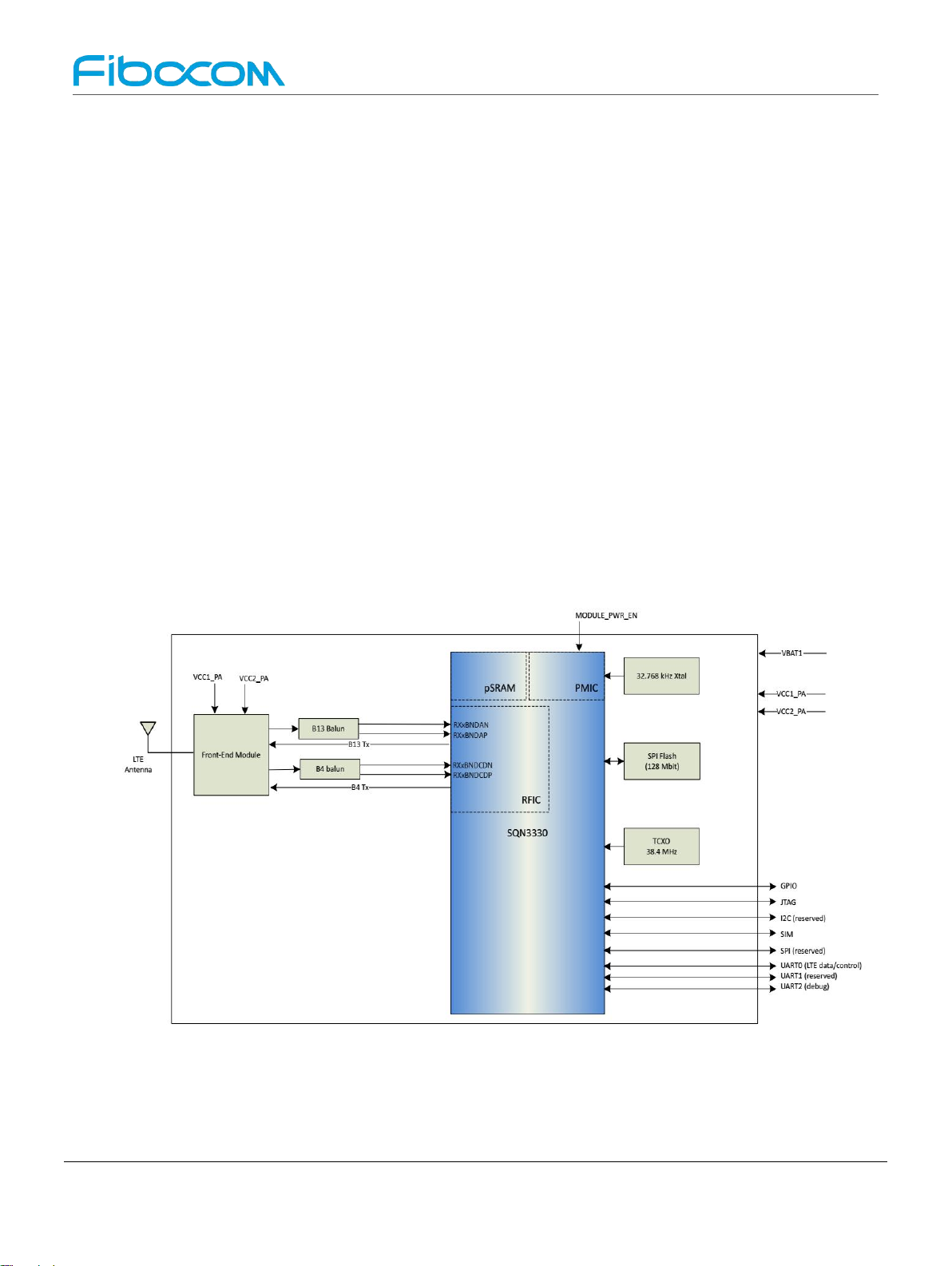
1 Product Features
1.1
M210-AM-00
Features Description
M210-AM modules include Monarch SQN3330 Cat-M1 baseband, a complete
dual band RF front end, memory and required circuitry to meet 3GPP EUTRA (Long Term Evolution - LTE, Release 13 set of specifications) and
Verizon Wireless LTE Cat-M1 UE specifications.
For more information on the core technology specifications see the section
References on page 3. The terms M210-AM module refer to the hardware
and the associated embedded software.
The architecture block diagram of the M210-AM is presented on Figure 1-1.
M210-AM Datasheet Page 8 of 38
Figure 1-1: M210-AM-00 Block Diagram
Reproduction forbidden without Fibocom Wireless Inc. written authorization - All Rights Reserved.

Table 1-1 on page 10 provides detail on general features of the M210-
AM.
Table 1-2 on page 11 provides detail for the LTE-related
features of the M210-AM.
M210-AM’s ECCN and part number are detailed in the Section 3.1 ECCN and
Part Number on page 15.
Table 1-1: General Features
General interfaces
•
JTAG
•
I2C (reserved)
•
USIM
•
SPI (reserved)
•
GPIO
•
UART (x3, including one reserved)
Supported Frequency Bands
•
LTE Band 4
•
LTE Band 13
Operation voltages
•
V
bat1
(range from 3.1 V to 4.5 V)
Packaging
•
LGA module
• 108 pads (21.35 x 20.25 x 1.79 mm)
•
RoHS compliant, halogen-free
Reproduction forbidden without Fibocom Wireless Inc. written authorization - All Rights Reserved.
M210-AM Datasheet Page 9 of 38

Reproduction forbidden without Fibocom Wireless Inc. written authorization - All Rights Reserved.
Operating temperature
•
RF compliant -30°C to +60°C (ambient)
•
Operational: -40°C to +85°C (board)
See also Section 3.3 Environmental Operating Conditions on page 19.
Humidity
• 10% to 85%
See also Section 3.3 Environmental Operating Conditions on page 19.
M210-AM Datasheet Page 10 of 38

Table 1-2: LTE Features
Standard compliance
•
3GPP E-UTRA Release 13 compliant
PHY
•
One UL and one DL transceiver
•
Support of HD-FDD Duplexing
•
Category M1 UE
•
Channel 1.4 MHz bandwidth
•
Normal and extended cyclic prefix
•
Support of MPDCCH
•
Modulation
-
DL: QPSK, 16QAM
-
UL: QPSK, 16QAM
•
All coding schemes corresponding to modulations
•
All channel coding (turbo-coding with interleaver, tail biting convolutional coding,
block and repetition coding) and CRC lengths
•
Sounding (including in special subframes)
•
Control and data in special subframes
•
All power control schemes and DL power allocation schemes
•
HARQ Incremental Redundancy and Chase Combining, with bundling or multi-
plexing
•
Measurements and computations related to CQI (Channel Quality Indicator), PMI
(Pre-coding Matrix Indicator) and RI (Rank Indicator), RSRP, and RSRQ
•
UEPCOP (from 3GPP Release 12) Power Saving Mode
MAC
•
Random Access procedure in normal and special subframes
•
Scheduling Request, Buffer Status Reporting, and Power Headroom Reporting
•
Discontinuous reception (DRX, eDRX) with long and short cycles
•
Fast scanning
•
Hosted configuration
•
IPv4, IPv6
•
RoHC
•
Location based services
•
Advanced QoS features
RLC
•
ARQ modes: UM, AM, and TM
PDCP
•
Ciphering and deciphering: NULL, AES, SNOW 3G
•
Integrity and protection: AES, SNOW 3G
RRC
•
MIB and new SIB1bis
•
Intra and inter-frequency measurements and handover
•
Up to 8 Data Radio Bearers supported
•
Support of CE (Coverage Extension) Mode
M210-AM Datasheet Page 11 of 38
Reproduction forbidden without Fibocom Wireless Inc. written authorization - All Rights Reserved.

Table 1-2: LTE Features (Continued)
NAS and above
•
NAS
•
SMS over SG
•
LWM2M Client
M210-AM Datasheet Page 12 of 38
Reproduction forbidden without Fibocom Wireless Inc. written authorization - All Rights Reserved.

Reproduction forbidden without Fibocom Wireless Inc. written authorization - All Rights Reserved.
2 FCC Regulation Warning
•
Manual Information To the End User
The OEM integrator has to be aware not to provide information to the end
user regarding how to install or remove this RF module in the user's
manual of the end product which integrates this module.
The end user manual shall include all required regulatory informa-
tion/warning as show in this manual.
•
Federal Communication Commission Interference Statement
This device complies with Part 15 of the FCC Rules. Operation is subject to
the following two conditions: (1) This device may not cause harmful inter-
ference, and (2) this device must accept any interference received,
including interference that may cause undesired operation.
This equipment has been tested and found to comply with the limits for a
Class B digital device, pursuant to Part 15 of the FCC Rules. These limits
aredesigned toprovide reasonableprotectionagainst harmfulinterference
in aresidential installation.This equipment generates,uses and can radiate
radio frequency energy and, if not installed and used in accordance with
theinstructions,may causeharmful interferenceto radiocommunications.
However, there is no guarantee that interference will not occur in a partic-
ularinstallation. Ifthis equipmentdoes causeharmful interferencetoradio
or televisionreception, whichcan be determined byturning theequipment
off and on, the user is encouraged to try to correct the interference by one
of the following measures:
–
Reorient or relocate the receiving antenna.
–
Increase the separation between the equipment and receiver.
–
Connect the equipment into an outlet on a circuit differentfrom that to
which the receiver is connected.
–
Consult the dealer or an experienced radio/TV technician for help.
Any changes or modificationsnot expressly approved by theparty respon-
sible for compliance could void the user's authority to operate this equip-
ment. This transmitter must not be co-located or operating in conjunction
with any other antenna or transmitter.
•
RadiationExposure Statement
This equipment complies with FCC radiation exposure limits set forth for
an uncontrolled environment. This equipment should be installed and
operatedwith minimum distance 20 cm between the radiator & your body.
M210-AM Datasheet Page 13 of 38

•
This device is intended only for OEM integrators under the following
conditions:
1.
The antenna must be installed such that 20 cm is maintained between the
antenna and users,
2.
The transmitter module may not be co-located with any other transmitter
or antenna.
3.
To complywith FCCregulationslimiting bothmaximum RFoutput power
•
10 dBi in 700 MHz Band
•
6 dBi in 1700 MHz Band
Assuming collocated with an ordinaryWLAN/WiMaxtransmitter with 34
dBm average EIRP power
•
6.5 dBi in Cellular band
•
6 dBi in PCS band
Remark: This assumption is not valid if the output power of the collocated
WLAN/ WiMax transmitter is higher than 34 dBm.
4.
The product using this module must also comply with the maximum
antenna gain to meet FCC EMC and RF exposure related limits. The
modular grant lists those maximum gain values.
5.
The OEM integrator needs show that the product hosting this module
15.107 and 15.109, respectively).
End Product Labeling
When the module is installed in the host device, the FCC ID label must be
visible through a window on the final device or it must be visible when an
access panel, door or cover is easily re-moved. If not, a second label must
be placed on the outside of the final device that contains the following text:
"Contains FCC ID: ZMOM210AM".
The grantee's FCC ID can be used only when all FCC compliance requirements are met.
and human exposure to RF radiation, the maximum antenna gain
including cable loss in a mobile exposure condition must not exceed:
StandaloneCondition:
In theevent thatthese conditionscannot be met(for examplecertainlaptop
configurations or co-location with another transmitter), then the FCC
authorization is no longerconsidered valid and the FCCID cannot be used
on the final product. In these circumstances, the OEM integrator will be
responsible for re-evaluating the end product (including the transmitter)
and obtaining a separate FCC authorization.
needs to be compliant with radiated and conducted emissions limits for
unintentional radiators (digital devices) per 15B testing (limits in part
Reproduction forbidden without Fibocom Wireless Inc. written authorization - All Rights Reserved.
M210-AM Datasheet Page 14 of 38

Reproduction forbidden without Fibocom Wireless Inc. written authorization - All Rights Reserved.
3 Physical Characteristics
3.1
ECCN and Part Number
The ECCN and orderable partnumberof the M210-AM modules will be
provided in a future revision of the document.
M210-AM Datasheet Page 15 of 38

3.2
Electrical Operating Conditions
3.2.1
Detailed Information
Table 3-1: Electrical Operating Conditions for M210-AM
Direction
Minimum
Typical
Maximum
VBAT1
In
3.1 V
4.5 V
SIM_VCC (1.8 V or 3.0 V)
Out
1.62 V
1.8 V
1.98 V
2.7 V
3.0 V
3.3 V
1V8
See note below.
Out
1.71 V
1.8 V
1.89 V
3V0
Out
2.85 V
3.0 V
3.15 V
VCC1_PA
In
2.85 V
3.0 V
3.3 V
VCC2_PA
In
2.85 V
3.0 V
3.3 V
3.2.2
M210-AM Power Tree
Figure 3-1 provides a representation of the power tree of the M210-AM.
Note: 1.
The maximum current consumption allowed from the 1V8 refer-
ence pin is 100 mA.
2.Each output reference voltage (1V8, 3V0) can be either running
or powered off depending on the internal software
configuration. They should not be used to power external IC or
parts that require permanent supply.
M210-AM Datasheet Page 16 of 38
Reproduction forbidden without Fibocom Wireless Inc. written authorization - All Rights Reserved.

Figure 3-1: M210-AM Power Tree
Reproduction forbidden without Fibocom Wireless Inc. written authorization - All Rights Reserved.
M210-AM Datasheet Page 17 of 38

3.2.3
Power Supplies Environment
Figure 3-2 illustrates the connections between the RF front-end power
supplies of the M210-AM.
Figure 3-2: M210-AM LTE RF Front-End Power Supplies Diagram
M210-AM
M210-AM Datasheet Page 18 of 38
Reproduction forbidden without Fibocom Wireless Inc. written authorization - All Rights Reserved.

Reproduction forbidden without Fibocom Wireless Inc. written authorization - All Rights Reserved.
3.3
Environmental Operating Conditions
3.3.1
Temperature
•
RF compliant: -30°C to +60°C (ambient)
•
Operational, with additional software to limit TxPower: -40°C to +85°C
(measured on board)
•
Storage: -40°C to +85°C
3.3.2
Humidity
•
Operating: 10% to 85% (non condensing)
•
Storage: 5% to 85% (non condensing)
M210-AM Datasheet Page 19 of 38

3.4
Power Supply Dimensioning
Important: - Information provided here is estimated peak current consump-
-
Average and detailed power consumption figures are provided
Estimated
Peak Power
Consumption
Estimated Battery Peak
Current (for
V
BAT1
=4.2 V)
TX
TX Power = 23 dBm
1.8 W
430 mA
TX Power = 20 dBm
1.6 W
380 mA
TX Power = 18 dBm
1.5 W
360 mA
TX Power = 13 dBm
1.3 W
310 mA
RX
1.1 W
260 mA
tion for the M210-AM Module in various LTE Tx/Rx
configurations, with and without DC/DC losses.
in Sequans’ Software Release Notes.
Table 3-2: Estimated Peak Current and Peak Power Consumption
(LTE Band 13)
Reproduction forbidden without Fibocom Wireless Inc. written authorization - All Rights Reserved.
M210-AM Datasheet Page 20 of 38

3.5
I/O Characteristics
The voltage and current characteristics of the various IO pads of the M210-
AM versus IO bank supply voltage are illustrated in the tables below.
Caution:
Refer to M210-AM Pin List to know the type of IO pad used on every
termination.
•
The Minimum values for Ioland Iohshould not be exceeded to guarantee
•
The Nominal valuesfor Ioland Iohrepresentthe nominal values for thepad
•
The Maximum values for Ioland Iohrepresent the maximal values for the
that the logical level are not spoiled for each pad type.
type. They are provided for information only.
pad type. They are provided for information only.
Note that the Vohvalues in the tables below do not apply to
GPIOsconfiguredin open drainmode.GPIOscan beindividually
configured in open drain mode. When in open drain mode they
either drive the line to Vol, or leave it floating, to be pulled up by
an externalpullup resistance. ThePCB designer must ensure that
the voltage on these pads never exceeds Vihof the IO group to
which they belong.
Reproduction forbidden without Fibocom Wireless Inc. written authorization - All Rights Reserved.
M210-AM Datasheet Page 21 of 38

Table 3-3: DC Characteristics for Digital IOs, Voltage 1.8 V
Parameter
Drive
Strength
Min.
Nom.
Max.
Unit
V
IL
Input Low Voltage
-0.3
0.63
V
V
IH
Input High Voltage
1.17
3.6
V
V
T
Threshold Point
0.79
0.87
0.94
V
V
T+
Schmitt Trigger Low to High Threshold Point
1
1.12
1.22
V
V
T-
Schmitt Trigger High to Low Threshold Point
0.61
0.71
0.8
V
V
T PU
Threshold Point with Pull-up Resistor Enabled
0.79
0.86
0.93
V
V
T PD
Threshold Point with Pull-down Resistor Enabled
0.8
0.87
0.95
V
V
T+ PU
Schmitt Trigger Low to High Threshold Point with
Pull-up Resistor Enabled
1
1.12
1.21
V
V
T- PU
Schmitt Trigger High to Low Threshold Point with
Pull-up Resistor Enabled
0.61
0.7
0.8
V
V
T+ PD
Schmitt Trigger Low to High Threshold Point with
Pull-down Resistor Enabled
1.01
1.13
1.23
V
V
T- PD
Schmitt Trigger High to Low Threshold Point with
Pull-down Resistor Enabled
0.62
0.72
0.81
V
I
I
Input Leakage Current @ VI=1.8V or 0V
±10
µA
I
OZ
Tri-state Output Leakage Current @ VO=1.8V or 0V
±10
µA
Input Capacitance
3
pF
Reproduction forbidden without Fibocom Wireless Inc. written authorization - All Rights Reserved.
M210-AM Datasheet Page 22 of 38

Table 3-3: DC Characteristics for Digital IOs, Voltage 1.8 V - BIDIR and IN Types
Parameter
Drive
Strength
Min.
Nom.
Max.
Unit
R
PU
Pull-up Resistor
5689148
kOhm
R
PD
Pull-down Resistor
5290167
kOhm
V
OL
Output Low Voltage
0.45
V
V
OH
Output High Voltage
1.35
V
I
OL
Low Level Output Current at VOL(max)
2 mA
1.2
2.2
3.6mA4 mA
2.3
4.3
7.1mA8 mA
4.6
8.6
14.3
mA
I
OH
High Level Output Current at VOH(max)
2 mA
1.0
2.4
4.6mA4 mA
2.0
4.7
9.2
mA
8 mA
4.0
9.4
18.4
mA
Parameter
Drive
Strength
Min.
Nom.
Max.
Unit
V
IL
Input Low Voltage
-0.3
0.4
V
V
IH
Input High Voltage
1.1
VBAT1 +
0.3
V
Parameter
Min.
Nom.
Max.
Unit
V
IL
Input Low Voltage
0.2
V
Table 3-4: DC Characteristics for IN_PMU Type
Table 3-5: DC Characteristics - BIDIR_WAKE Type
M210-AM Datasheet Page23of
Reproduction forbidden without Fibocom Wireless Inc. written authorization - All Rights Reserved.
38

P
ERFORMANCE
Table 3-5: DC Characteristics - BIDIR_WAKE Type (Continued)
Parameter
Min.
Nom.
Max.
Unit
V
IH
Input High Voltage. See note below related to
maximum value.
0.8
3.6
V
V
OL
Output Low Voltage
0
V
V
OH
Output High Voltage
1.6
1.8
V
P
HYSICALCHARACTERISTICS
Reproduction forbidden without Fibocom Wireless Inc. written authorization - All Rights Reserved.
M210-AM Datasheet Page 24 of 38

3.6
Performance
Table 3-5 and Table 3-6 present the M210-AM module’s performance in LTE
Band 4 and Band 13.
Table 3-5: Output Power
LTE Band
Frequency (kHz)
TCH
Conducted Power (dBm)
Bandwidth 1.4 MHz, Full
RB
Band 13
779500
23205
23 +2/-2.7
782000
23230
23 +2/-2.7
784500
23255
23 +2/-2.7
Band 4
1712500
19975
23 +2/-2.7
1732500
20175
23 +2/-2.7
1752500
20375
23 +2/-2.7
LTE Band
Frequency (kHz)
TCH
Typ. Sensitivity level
(dBm)
Bandwidth 1.4 MHz
Band 13
748500
5205
-103
751000
5230
-103
753500
5255
-103
Band 4
2112500
1975
-103
2132500
2175
-103
2152500
2375
-103
Table 3-6: RF Sensitivity
M210-AM Datasheet Page 25 of 38
Reproduction forbidden without Fibocom Wireless Inc. written authorization - All Rights Reserved.

3.7
Component Reliability
Note:
3.8
Package Description
3.8.1
Module Footprint
The dimensions marked in Figure 3-4 are listed in Table 3-7.
Information relatedto component reliability will beprovided in a
future edition of this document.
Figure 3-4: Top and Side View of the M210-AM
Reproduction forbidden without Fibocom Wireless Inc. written authorization - All Rights Reserved.
M210-AM Datasheet Page 26 of 38

Table 3-7: M210-AM Outline Dimensions
Mark
Minimum (mm)
Nominal (mm)
Maximum (mm)
A
21.25
21.35
21.45
B
20.15
20.25
20.35
C
1.71
1.79
1.94
D
Not Available
Not Available
0.08
M210-AM Datasheet Page 27 of 38
Reproduction forbidden without Fibocom Wireless Inc. written authorization - All Rights Reserved.

The dimensions marked in Figure 3-5 are listed in Table 3-8.
Mark
Dimension and tolerance (mm)
L
21.35 ± 0.1
W
20.25 ± 0.1
A1
12 ± 1.0
A2
4.125 ± 0.5
A3
10.8 ± 1.0
A4
4.725 ± 0.5
M210-AM Datasheet Page 28 of 38
Figure 3-5: M210-AM Bottom Side View of Pads
Table 3-8: M210-AM Dimensions and Tolerances
Reproduction forbidden without Fibocom Wireless Inc. written authorization - All Rights Reserved.

Table 3-8: M210-AM Dimensions and Tolerances (Continued)
Mark
Dimension and tolerance (mm)
A5
0.6 ± 0.05
A6
1.2 ± 0.1
A7
0.6 ± 0.05
B1
0.9 ± 0.1
B2
0.325 ± 0.05
B3
0.6 ± 0.05
B4
19.2 ± 0.2
B5
18 ± 0.2
B6
1.075 ± 0.1
B7
1.675 ± 0.15
C1
6.125 ± 0.5
C2
6.8 ± 0.5
C3
1.2 ± 0.01
C4
0.5 ± 0.05
D1
0.5 ± 0.05
D2
0.9 ± 0.1
D3
7 ± 0.5
D4
6.725 ± 0.5
D5
18.9 ± 0.2
D6
15.9 ± 0.2
M210-AM Datasheet Page 29 of 38
Reproduction forbidden without Fibocom Wireless Inc. written authorization - All Rights Reserved.

3.8.2
Marking Information
Figure 3-6: M210-AM-00 Marking Description
3.9
Packing Information
3.10
Storage Conditions
1.
Calculated shelf life in sealed bag : 12 months at < 40°C and < 90% RH
2.
Peak package body temperature: 250°C
3.
After bag is opened, devices thatwill be subjected to reflow solder or other
high temperature process must be:
The module is delivered in Tape-and-Reel.
Note:
Note:
Reproduction forbidden without Fibocom Wireless Inc. written authorization - All Rights Reserved.
M210-AM Datasheet Page 30 of 38
Details about packingofthe moduleswill be provided in a future
revision of this document.
Additional storage conditions impacting the mounting process
are providedinSection 3.11Mounting Considerations on page31.

a)
mounted within 168 hours of factory conditions ≤ 30°C/60%RH, or
b)
Stored as per J-STD-033
4.
Devices require bake, before mounting, if
a)
HumidityIndicator Card reads >10%for level2a-5a devicesor >60%for
level 2 devices when read at 23±5°C
b)
3a or 3b above are not met
5.
If baking is required, refer to IPC/FEDEC J-STD-033 for bake procedure.
Note:
3.11
Mounting Considerations
Note:
Details will be provided in a future revision of this document.
The M210-AM can support up to 3 reflows with 250°C maximum.
Parameter
Setting
Peak package body temperature
To be defined
Liquidous Time
To be defined
Preheat/Soak
To be defined
Ramp-up rate
To be defined
Ramp-down rate
To be defined
This section provides reflow information.
Table 3-10: Reflow Parameters
Level and body temperature are defined by IPC/JEDEC
J-STD-020.
Reproduction forbidden without Fibocom Wireless Inc. written authorization - All Rights Reserved.
M210-AM Datasheet Page 31 of 38

4 Signal and Pins
4.1
M210-AM Pinout
The signals and all the related details are listed in the MS-Excel companion
file delivered together with the present document in a PDF portfolio.
The pads listed in Table 4-1 are connected to ground.
Pad #
Pad
Name
Comment
1 20 22 24 26 28 30 31 32 33 34 42 43 45 46
53
55 62 63 64 65 66 68 69 70 71 72 73 74 86 87
GND
All GND pads shall be connected to the
same copper.
T1 T2 T3 T4 T5 T6 T7 T8 T9 T10 T11
T12 T13 T14 T15 T16 T17 T18 T19 T20
T21 T22 T23 T24 T25 T26 T27 T28 T29
T30
GND
T1 to T30 pads are used as both GND and
thermal drops.
Table 4-1: Ground and Thermal Pads
Reproduction forbidden without Fibocom Wireless Inc. written authorization - All Rights Reserved.
M210-AM Datasheet Page 32 of 38

4.2
UART Interfaces
4.2.1
High-Speed UARTs
Figure 4-1 representsthe typical implementation for thehardware flowcontrol
M210-AM are designed for use as DCE (Data Communication Equipment).
•
Port TXD on Application sends data to the module’s TXD signal line.
•
Port RXD on Application receives data from the module’s RXD signal line.
Note:
CLK signals can be input or output.
4.3
Power-up Sequence
M210-AM
for UART0, UART1 and UART2. TDX and RDX signals are mandatory. RTS
and CTS are strongly recommended.The other signals are optional.
Based on the conventions for DCE-DTE connections, the DCE device will
communicate with the customer application (DTE) using the following
signals:
M210-AM Datasheet Page 33 of 38
Figure 4-1: UART0, UART1 and UART2 Signals Convention and Flow
Control
Reproduction forbidden without Fibocom Wireless Inc. written authorization - All Rights Reserved.

The following timing requirement applies to the signals VBAT1,
MODULE_PWR_EN and RESET_N. It must be respected for proper M210-
AM’sbehavior.
Figure 4-3: VBAT1, MODULE_PWR_EN and RESET_N Signals Timing
Symbol
Description
Minimum Duration
Maximum Duration
ts
VBAT1 setup time
1 ms
-
ts1
RESET_N setup time
1 ms
-
th1
RESET_N hold time
1 µs
-
Requirement for Cold Start
Figure 4-4: VBAT1, MODULE_PWR_EN and RESET_N Signals Timing
Requirement for Warm Start
Figure 4-5: VBAT1, MODULE_PWR_EN and RESET_N Signals Timing
Requirement for Reset Cycle
The timing minimum values are listed in Table 4-3.
Table 4-3: VBAT1, MODULE_PWR_EN and RESET_N Signal Timing Values
M210-AM Datasheet Page 34 of 38
Reproduction forbidden without Fibocom Wireless Inc. written authorization - All Rights Reserved.

4.4
LTE Low Power Mode
Important: The M210-AM module is provided with an internal RTC whose
The M210-AM will automatically enter in low-power mode. M210-AM can be
woken from low power mode by external sources through:
•
SIM_DETECTinput signal to cope with SIM card insertion into a SIM card
connector with built-in hardware detection. The default configuration to
wake-up the module is a low-to-high transition.
•
The RTS0 input signal whenever data traffic is initiated by the host
connected to the module UART0 with hardware flow control; The default
configuration to wake-up the module is a high-to-low transition.
•
Two dedicated input signal WAKE0 and WAKE1; The default configura-
tion to wake-up the module is on a high-to-low transition. This can be
modified by software. As example, these signals can be used to detect an
alarm from an external IC such as a sensor. Software can disable the
wake-up functionality on these signals.
•
A subset of GPIO input signals:GPIO2, GPIO3, GPIO25,GPIO27, GPIO42;
they are not configured by default as wake-up source but software can
configure them for future use.
•
Pads that are not driven by an external device shall be driven low by soft-
ware if they have a GPIO or RFDATA mode that allows it.
•
For pads that are known to be driven by an external device:
Configure that external device to hold the signal stable during low-power
mode, and configure M210-AM to treat that pin as an input, without
internal pull-up or pull-down.
•
For pads where,at the time of low-power mode, the signal may or may not
be driven by an external device:
ConfigureM210-AM to enable theinternal pull-up/pull-down on thepad to
guarantee that it will not be floating during low-power mode.
supply is VBAT1. As a consequence, VBAT1 should not be
removed, in order to keep RTC active.
Important: WAKE inputs are detected on level (configurable by software
to 0 or 1) that must last at least 5 periods of the 32 kHz clock,
that is 156.25 ìs.
Toget the lowest possible power consumption during low-power mode, all
IOs must be stable. At software configuration time, take care of the following,
to prevent them from being in conflict or floating:
Note:
Reproduction forbidden without Fibocom Wireless Inc. written authorization - All Rights Reserved.
M210-AM Datasheet Page 35 of 38
Each signal’s pull (up or down) is determined by register. It can
be modified by software. Please see the default configuration in
the signal’s list.

Reproduction forbidden without Fibocom Wireless Inc. written authorization - All Rights Reserved.
A Acronyms
Acronym
Definition
AFE
Analog Front-End
APC
Automatic Control Power
APT
AveragePower Tracking
CE
Coverage Extension
COO
Country of origin
CPU
Central Processing Unit
DC/DC
Direct current converter
DL
Downlink
DPLL
Digital Phase-Locked Loop
ECCN
Export Control Classification Number
EPS
Evolved Packet System
ESD
Electro-static discharge
ETSI
European Telecommunications Standard Institute
GND
Ground
GNSS
Global Navigation Satellite System. Superset for systems such as GPS, Galileo,
Glonass, BeiDou or QZSS among others.
GPIO
General Purpose Input Output
HBM
Human Body Model (ESD)
I/O
Input/Output
I2C
Inter-integrated circuit (bus)
M210-AM Datasheet Page 36 of 38

Reproduction forbidden without Fibocom Wireless Inc. written authorization - All Rights Reserved.
Acronym
Definition
IMEI
International Mobile Equipment Identity
IMS
Instant Messaging Service
IP
Internet Protocol
JTAG
Joint Test Action Group. See IEEE 1149.7 specification
LDO
Low Drop-Out regulator
LGA
Large Grid Array
LNA
Low-Noise Amplifier
LTE
Long Term Evolution, or 4G. Standard is developed by the 3GPP
www.3gpp.org
.
MM
Machine Model (ESD)
NAS
Network Access Server
NVM
Non Volatile Memory
OMADM
Open Mobile Alliance Device Management
PCB
Printed Circuit Board
PHY
Physical Layer
PLL
Phase-Locked Loop
PMIC
Power Management Integrated Circuit
pSRAM
Pseudo-Static Random Access Memory
QTY
Quantity
RAM
Random Access Memory
RB
Resource Block
RF
Radio Frequency
RFIC
RF Integrated Circuit
RoHS
Restriction of Hazardous Substances
RTC
Real-Time Clock
Rx
Reception
M210-AM Datasheet Page 37 of 38

Reproduction forbidden without Fibocom Wireless Inc. written authorization - All Rights Reserved.
Acronym
Definition
S/N
or SN: Serial Number
SAW
Surface Acoustic Wave(filters)
SDM
Socketed Device Model (ESD)
SIM
Subscriber Identification Module
SMS
Short Message Service
SPI
Serial Peripheral Interface
TCXO
Temperature-controlledcrystal oscillator
Tx
Transmission
UART
Universal asynchronous receiver transmitter.
UE
User Equipment
UICC
Universal integrated circuit card (SIM)
UL
Uplink
XTAL
Crystal
M210-AM Datasheet Page 38 of 38
 Loading...