

Page 1

L850-GL Hardware User Manual
Version:V1.0.3
Update date:2/25/2017
Page 2

forbidden without Fibocom Wireless Inc. written authorization
All Rights Reserved.
Applicability Table
No. Product model
1
L850-GL
Description
NA
L850-GL Hardware User Manual
Reproduction
-
Page 2 of 51
Page 3
forbidden without Fibocom Wireless Inc. written authorization
Copyright © 2017Fibocom Wireless Inc. All rights reserved.
permission of the copyright holder, any company or individual is prohibited to
excerpt, copy any part of or the entire document, or distribute the document in any form.
The document is subject to update from time to time owing to the product vers
reasons. Unless otherwise specified, the document only serves as the user guide. All the statements,
information and suggestions contained in the document do not constitute any explicit or implicit guarantee.
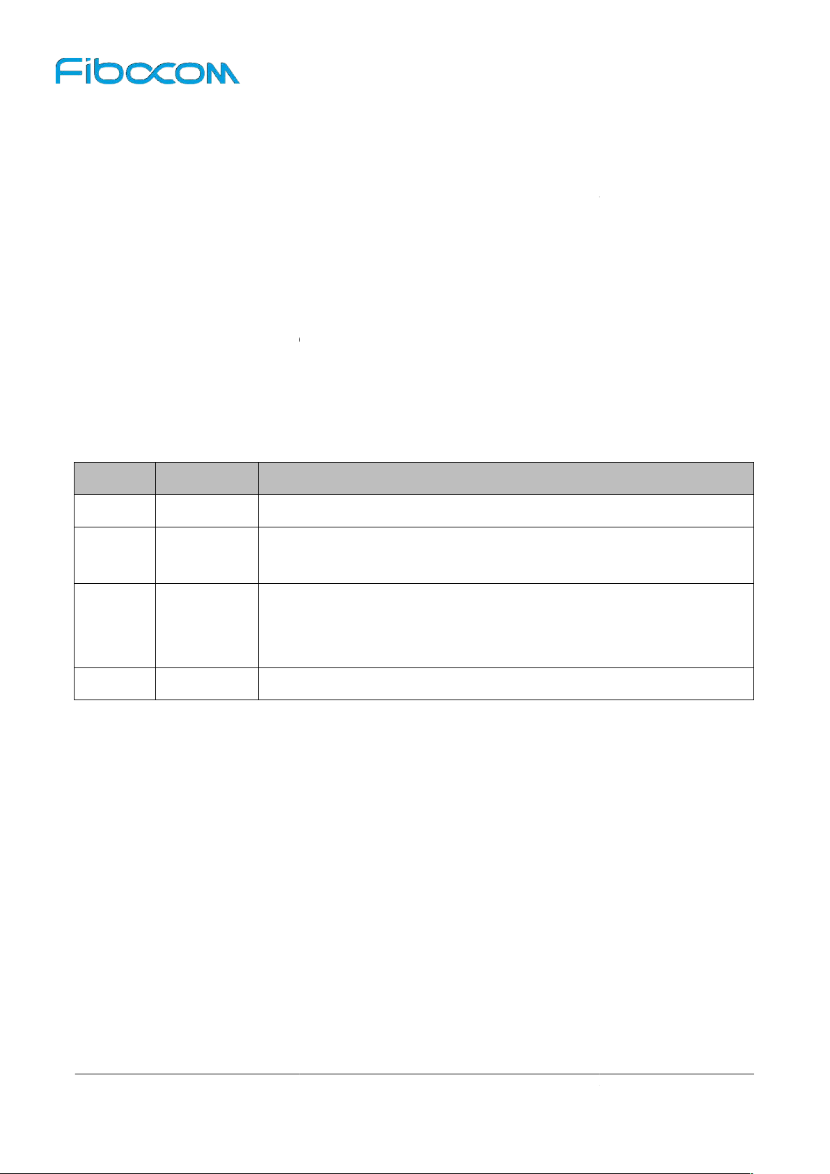
Remark
Modify the PCIe Interface Application;
Update the Pin Definition: change pin65 to NC
Modify the description
Update the content of PCIe
Add the power Consumption of 3CA
Add product certification of warnings
All Rights Reserved.
Copyright
Without the prior written
Notice
ion upgrade or other
Version Record
Version Update date
V1.0.0 2016-12-08 Draft
V1.0.1
2016-12-16
V1.0.2
V1.0.3 2017-02-25
2017-02-09
L850-GL Hardware User Manual
Reproduction
-
Page 3 of 51
Page 4

forbidden without Fibocom Wireless Inc. written authorization
................................
................................
................................
................................
................................
................................
................................
................................
................................
................................
................................
................................
................................
................................
................................
................................
................................
................................
................................
................................
................................
Power Consumption
................................
................................
................................
Sequence
................................
................................
................................
Definition
Application
................................
Definition
All Rights Reserved.
................................
................................
................................
................................
................................
................................
................................
................................
................................
................................
................................
................................
................................
................................
................................
................................
................................
................................
................................
................................
................................
................................
................................
................................
................................
................................
................................
................................
................................
................................
................................
................................
................................
Contents
1
Foreword
................................................................
.......... 7
1.1 Introduction
1.2 Reference Standard
1.3 Related Documents
2
Overview
2.1 Introduction
2.2 Specification
2.3 Warnings
2.3.1
2.3.2
2.3.3
2.4 CA combinations
FCC Statement
IC Statement
CE Statement
2.5 Application Framework
2.6 Hardware Framework
3
Application Interface
3.1 M.2Interface
................................................................
................................................................
................................................................
................................................................
................................................................
................................................................
................................
................................
................................
................................
................................
................................
................................
................................
................................
.......... 7
........................... 7
............................ 7
.......... 8
.......... 8
........ 8
.............. 9
................................ 9
.................................. 11
................................ 12
............................... 13
.................... 14
...................... 15
................... 15
....... 15
3.1.1
Pin Distribution
3.1.2
Pin Definition
3.2 Power Supply
3.2.1
Power Supply
3.2.2
Logic level
3.2.3
3.3 Control Signal
3.3.1
Module Start-Up
3.3.1.1
3.3.1.2
3.3.2
Module Shutdown
3.3.3
Module Reset
Start-upCircuit
Start-upTiming
3.4 USB Interface
3.4.1
USB Interface
3.4.2
USB2.0 Interface
................................................................
................................................................
................................
................................
................................................................
................................
................................................................
................................................................
................................
................................................................
................................................................
................................
................................
................................................................
................................................................
.............................. 16
.................................. 17
.... 21
................................. 21
...... 22
..................... 23
.... 25
............................ 25
............... 25
........................... 25
......................... 26
................................. 27
.... 28
............... 28
...... 28
3.5 PCIe Interface
3.5.1
L850-GL Hardware User Manual
PCIe Interface
Reproduction
................................................................
................................
................................... 29
.............. 29
-
Page 4 of 51
Page 5

forbidden without Fibocom Wireless Inc. written authorization
Application
................................
................................
Circuit
Slot
Slot
................................
................................
................................
................................
................................
................................
................................
................................
................................
................................
................................
................................
................................
................................
................................
nctionality
RFConnector Characteristic
Dimension
................................
................................
................................
................................
................................
................................
................................
................................
................................
................................
................................
All Rights Reserved.
................................
................................
................................
................................
................................
................................
................................
................................
................................
................................
................................
................................
................................
................................
................................
................................
................................
................................
................................
................................
................................
................................
................................
................................
................................
................................
................................
................................
................................
................................
................................
................................
................................
................................
................................
3.5.2
PCIe Interface
................................................................
........... 29
3.6 USIMInterface
3.6.1
3.6.2
3.6.3
3.6.4
3.7 Status Indicator
3.7.1
3.7.2
3.7.3
USIM Pins
USIM Interface
3.6.2.1
3.6.2.2
USIM Hot-Plugging
USIM Design
LED#1Signal
WOWWAN#
TX_BLANKING
3.8 Interrupt Control
3.8.1
W_DISABLE1#
3.8.2
BODYSAR
3.9 ClockInterface
N.C. SIMCard
N.O. SIM Card
................................................................
................................................................
................................................................
................................
................................................................
................................
................................
................................
................................
................................
................................
................................
................................
................................................................
................................
................................... 31
...... 31
.................. 32
........................................ 32
...................................... 32
....................... 33
.................................. 34
................................. 34
.................................. 35
................................... 35
.............................. 36
................................ 36
.............................. 36
...... 37
................................... 37
3.10 ANT Tunable Interface
3.11 Config Interface
3.12 Other Interfaces
4
Radio Frequency
4.1 RF Interface
4.1.1
4.1.2
4.1.3
4.2 Operating Band
4.3 Transmitting Power
4.4 Receiver Sensitivity
4.5 GNSS
4.6 Antenna Design
5
Structure Specification
5.1 Product Appearance
RF Interface Fu
RF Connector
................................................................
................................................................
................................................................
................................................................
................................................................
................................
................................
................................
................................
................................
................................
................................
................................
................................
................................
.................. 37
.............................. 38
.............................. 38
.......................... 39
....... 39
............ 39
........ 39
............. 39
................................. 41
.......................... 42
.......................... 43
................. 44
................................ 45
.............. 47
........................ 47
5.2 Dimension of Structure
5.3 M.2 Interface Model
5.4 M.2 Connector
5.5 Storage
L850-GL Hardware User Manual
Reproduction
................................................................
................................
................................
................................
.................... 47
.......................... 48
................................... 48
............... 49
-
Page 5 of 51
Page 6

forbidden without Fibocom Wireless Inc. written authorization
................................
................................
................................
................................
All Rights Reserved.
................................
................................
................................
................................
5.5.1
Storage Life
................................
.................................... 49
5.6 Packing
5.6.1
Tray Package
5.6.2
Tray size
................................................................
................................
................................................................
............... 49
................................. 50
......... 51
Reproduction
L850-GL Hardware User Manual
-
Page 6 of 51
Page 7

forbidden without Fibocom Wireless Inc. written authorization
The document describes the electrical characteristics, RF performance, dimensions and application
(hereinafter referred to as L850). With the assistance of the document and
other instructions, the developers can quickly understand the hardware functions of L850 modules and
Standard
The design of the product complies with
1 V10.8.0: User Equipment (UE) conformance specification;Radio transmission
and reception (FDD);Part 1: Conformance specification
3GPP TS 34.122 V10.1.0: Technical Specification Group Radio Access Network; Radio
ansmission and reception (TDD)
1 V10.6.0: User Equipment (UE) conformance specification; Radio transmission
and reception; Part 1: Conformance testing
3GPP TS 21.111 V10.0.0: USIM and IC card requirements
3GPP TS 51.011 V4.15.0: Specifica
3GPP TS 31.102 V10.11.0: Characteristics of the Universal Subscriber Identity Module (USIM)
3GPP TS 31.11 V10.16.0: Universal Subscriber Identity Module (USIM) Applic
3GPP TS 36.124 V10.3.0: ElectroMagnetic Compatibility (EMC) requirements for mobile terminals
3GPP TS 27.007 V10.0.8: AT command set for User Equipment (UE)
3GPP TS 27.005 V10.0.1: Use of Data Terminal Equipme
DCE) interface for Short Message Service (SMS) and Cell Broadcast Service (CBS)
PCI Express M.2 Specification Rev1.0
Documents
L850 Module Performance Testing Report
RF Antenna Application Design
Family System Driver Integration and Application Guidance
Family AT CommandsManual
All Rights Reserved.
Mobile Equipment
Data Circuit terminating Equipment
1
Foreword
1.1
Introduction
environment, etc. of L850-GL
develop products.
1.2
Reference
3GPP TS 34.121-
tr
3GPP TS 36.521-
(SIM-ME) interface
the following standards:
tion of the Subscriber Identity Module -
application
and ancillary equipment
(DTE -
1.3
Related
L8-
L8-
L850-GL Hardware User Manual
Reproduction
Specification
ation Toolkit(USAT)
nt -
-
Page 7 of 51
Page 8
forbidden without Fibocom Wireless Inc. written authorization
L850 is a highly integrated 4G wireless communication module that adopts standard PCIe M.2 interface
supports LTE FDD/LTE TDD/WCDMA/ system. It is applicable to most broadband communication
networks of the mobile operator across the world.
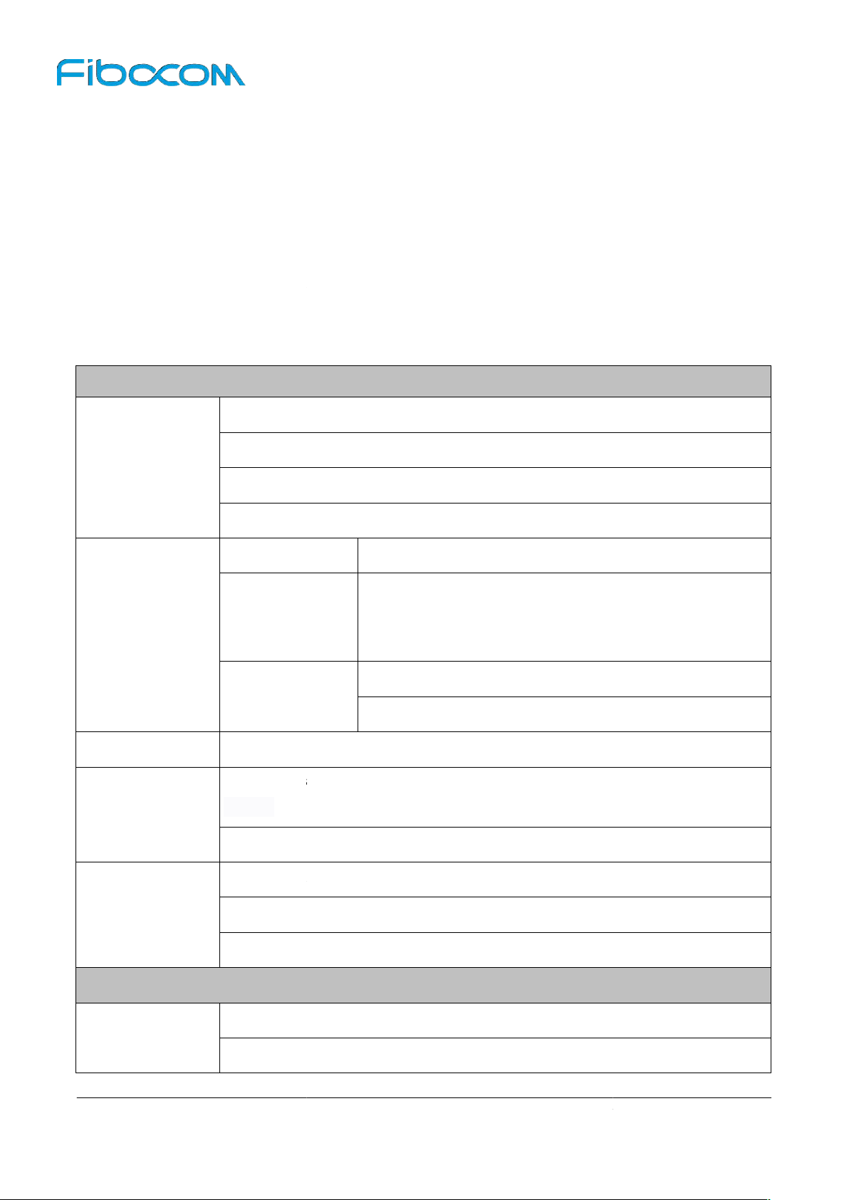
LTE FDD: Band 1,2,3,4,5,7,8,11,12,13,17,18,19,20,21,26,28,29,30,66
LTE TDD: Band 38, 39, 40, 41
WCDMA/HSPA+: Band 1,2,4,5,8
GNSS/Beidou: support
UMTS/HSPA+
~
Normal operating temperature:
operating temperature:
Storage temperature:
Interface: M.2 Key
:
Weight: About5.8 g
WWAN Main Antenna x 1
WWAN Diversity Antenna x 1
All Rights Reserved.
When LTE TDD achieves maximum DL rate, its UL rate can
HSDPA+:42Mbps DL(Cat 24)/5.76Mbps UL(Cat6)
2
Overview
2.1
Introduction
and
2.2
Specification
Specification
Operating Band
Data Transmission
LTE FDD
LTE TDD
450Mbps DL/50Mbps UL(Cat 9)
260Mbps DL/30Mbps UL(Cat 9)
reach 10Mbps only
UMTS:384 kbps DL/384 kbps UL
DC-
Power Supply
Temperature
Physical
characteristics
Interface
Antenna
L850-GL Hardware User Manual
Reproduction
DC 3.135V
Expand
Dimension
4.4V,Typical 3.3V
-10°C ~+55°C
-20°C ~+70°C
-40°C ~+85°C
-B
30 x 42 x 2.3mm
-
Page 8 of 51
Page 9
forbidden without Fibocom Wireless Inc. written authorization
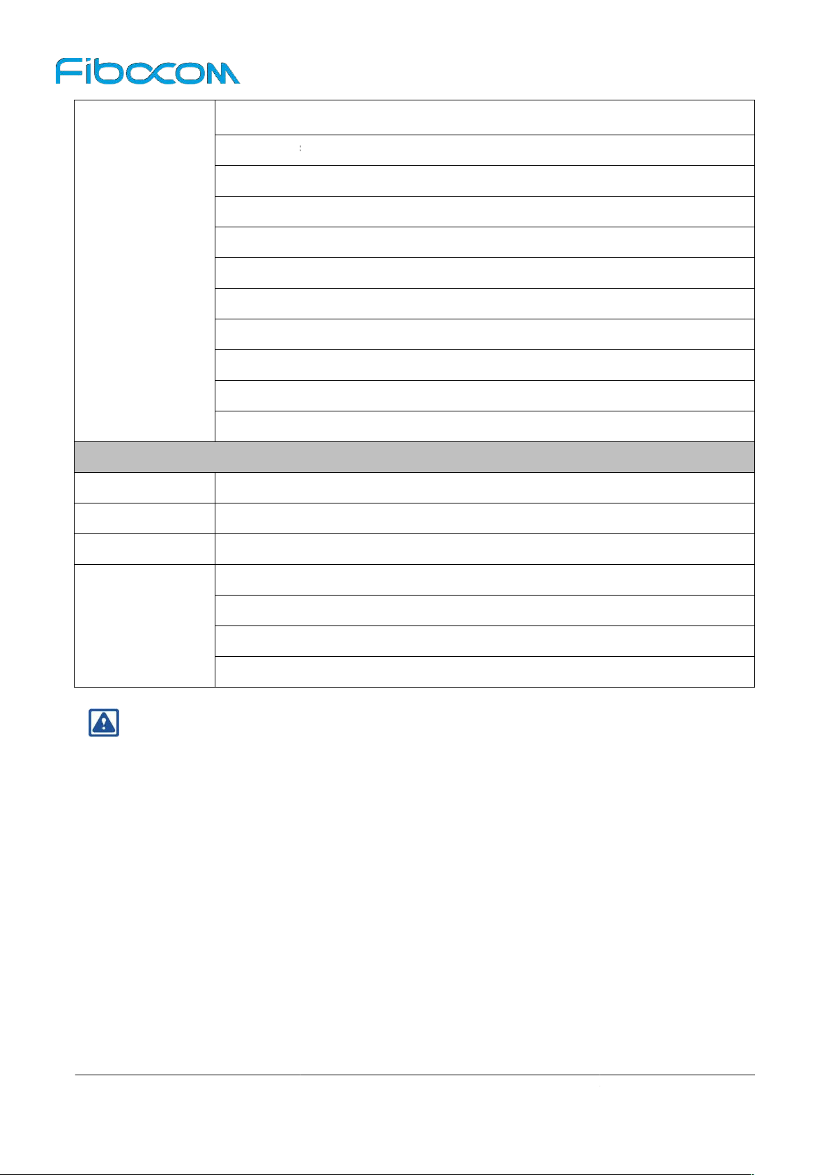
3V/1.8V
just for debugging
Tunable antenna
I2S(Reserved)
I2C(Reserved)
USB3.0(not supported yet)
3GPP TS 27.007 and 27.005
Multiple carrier
Windows MBIM support
Windows update
For normal operating temperature, LTE FDD Band 4 and 13 can support the temperature
to +60
Communication Commission Interference Statement
This device complies with Part 15 of the FCC Rules. Operation is subject to the following two
(1) This device may not cause harmful interference, and (2) this device must accept any interferenc
received, including interference that may cause undesired operation.
All Rights Reserved.
Function Interface
Software
USIM
USB 2.0
PCIe 1.0 X1
W_Disable#
BodySar
LED
Clock
(
)
Protocol Stack
AT commands
Firmware update PCIe
IPV4/IPV6
Other feature
AGNSS
Note:
ranging from -20℃
2.3
Warnings
℃.
2.3.1
FCC Statement
L850-GL Hardware User Manual
Reproduction
Federal
-
conditions:
e
Page 9 of 51
Page 10

Reproduction forbidden without Fibocom Wireless Inc. w
This equipment has been tested and found to comply with the limits for a Class B digital device, pursuant
to Part 15 of the FCC Rules. These limits are designed to pr
interference in a residential installation. This equipment generates, uses and can radiate radio frequency
energy and, if not installed and used in accordance with the instructions, may cause harmful interference
to radio communications. However, there is no guarantee that interference will not occur in a particular
installation. If this equipment does cause harmful interference to radio or television reception, which can
be determined by turning the equipment off
interference by one of the following measures:
Reorient or relocate the receiving antenna.
Increase the separation between the equipment and receiver.
Connect the equipment into an outlet on a circu
to which the receiver is connected.
Consult the dealer or an experienced radio/TV technician for help.
Any changes or modifications not expressly approved by the party responsible for compliance could
authority to operate this
located or operating in conjunction with any other antenna or
This equipment complies with FCC radiation exposure limits set forth for an unc
This equipment should be installed and operated with
This device is intended only for OEM integrators under the following conditions:
The antenna must be installed such that 20
users, and the maximum antenna gain allowed for use with this device is 5
The transmitter module may not be co
As long as 2 conditions above are met, further
integrator is still responsible for testing their end
All Rights Reserved.
and on, the user is encouraged to try to correct the
cm is maintained between the antenna and
dBi.
antenna.
test will not be required. However, the OEM
product for any additional compliance requirements
it different from that
FCC Caution:
void the user's
equipment.
This transmitter must not be co-
transmitter.
Radiation Exposure Statement:
your body.
1)
2)
-located with any other transmitter or
transmitter
-
ontrolled environment.
between the radiator &
required with this module installed
L850-GL Hardware User Manual
ritten authorization -
Page 10 of 51
Page 11

Reproduction forbidden without Fibocom Wireless Inc. w
In the event that these conditions
another
used
evaluating the end product (including the transmi
This transmitter module is authorized only for use in device where the antenna may be installed such that
20 cm may be maintained between the antenna and users. The final end product m
Contains FCC ID: ZMOL850GL
only when all FCC compliance requirements are met.
Manual Information To the End User
The OEM integrator has to be aware not to provide information to the end user regarding how to install or
remove this RF module in the user’s manual of the end product which integrates this module. The end
user manual shall include all required regulatory
This device complies with Industry Canada license
this device may not cause interference,
this device must accept any interference, including interference that may cause undesired
Le présent appareil est conforme aux CNR d'Industrie Canada applicables aux
exempts de licence. L'exploitation
l'appareil ne doit pas produire de brouillage,
l'utilisateur de l'appareil doit accepter tout brouillage radioélectrique subi, même si le brouillage
est susceptible d'en compromettre le
This Class B digital apparatus complies with Canadian
Cet appareil numérique de la classe B est conforme à la norme NMB
This device complies with RSS
e does not cause harmful
la
condition que cet appareil ne provoque aucune interférence
All Rights Reserved.
(for example certain laptop
circumstances,
”. The grantee's FCC ID can be used
exempt RSS standard(s). Operation is
suivantes:
003 du
310 of Industry Canada. Operation is subject to the condition
la
L'opération
IMPORTANT NOTE:
can not be met
configurations or co-location with
valid and the FCC ID can not be
be responsible for re-
authorization.
transmitter), then the FCC authorization
on the final product. In these
is no longer considered
the OEM integrator will
End Product Labeling
visible area with the following: “
L
ust be labeled in a
2.3.2
IC Statement
Industry Canada statement
the following two conditions:
1)
2)
operation of the device.
1)
2)
est autorisée aux deux conditions
and
fonctionnement.
-
et
ICES-003.
-
Canada.
subject to
appareils radio
devic
Cet appareil est conforme à
L850-GL Hardware User Manual
-
interference.
norme RSS-310 d'Industrie Canada.
nuisible.
ritten authorization -
that this
est soumise à la
Page 11 of 51
Page 12

Reproduction forbidden without Fibocom Wireless Inc. w
antenna(s)
antenna or transmitter, except tested built
Cet appareil et son antenne ne doivent pas être situés ou fonctionner en conjonction avec
antenne ou un autre émetteur, ex
The County Code Selection feature is disabled for products marketed in the US/
l'indicatif
This equipment complies with IC radiation exposure limits set forth for an uncontrolled environment. This
equipment should be installed and operated with minimum distance 20cm between the radiator &
Déclaration d'exposition aux radiations:
Cet équipement est conforme aux limites d'exposition aux rayonnements IC établies pour un
environnement non contrôlé. Cet équipement doit être installé et utilisé avec un minimum de 20 cm de
re la source de rayonnement et votre corps.
Hereby, We, Manufacturer name declares that the radio equipment type L850
of the final product must be mass against the Essential requirements of the
Articles 3.1(a) and (b), safety and EMC respectively, as well as any relevant Article
is 5 dBi
Declaration of Conformity(should include manufacturer contact info.)
Please added certification standard in your user manual which depended on the test standards your
If the DoC should be a simplified ve
full text of the EU declaration of conformity is available at the following internet address: http//
All Rights Reserved.
conjunction
produits
GL is in compliance with
separation distance is 20cm.
This device and its
must not be co-located or operating in
with any other
La fonction de sélection de
États-Unis et au Canada.
-in radios.
du pays est désactivée pour les
une autre
testées.
Canada.
commercialisés aux
Radiation Exposure Statement:
body.
your
distance ent
IC : 21374-L850GL
2.3.3
► EU Regulatory Conformance
the Directive 2014/53/EU.
CE Statement
-
In all cases assessment
Directive 2014/53/EU
3.2 requirements.
The maximum antenna gain for
►
and the antenna
device performed.,
fibocom.com
L850-GL Hardware User Manual
The
www.
ritten authorization -
Page 12 of 51
Page 13
Reproduction forbidden without Fibocom Wireless Inc. w
GL is in conformity with the relevant Union
2014 / 53 / EUwith reference to the following standards applied:
Health (Article 3.1(a) of Directive 2014/53/EU)
Safety (Article 3.1(a) of Directive 2014/53/EU)
1: 2006 + A11: 2009 + A1: 2010 + A12: 2011 + A2: 2013
Electromagnetic compatibility (Article 3.1 (b) of Directive 2014/53/EU)
3 V2.1.0 /
usage (Article 3.2 of Directive 2014/53/EU)
2 V11.1.1 /V11.1.1
combination
All Rights Reserved.
harmonization legislation: Radio Equipment directive:
L850-
Applied Standard(s):
EN 62311 : 2008
Applied Standard(s):
EN 60950-
Applied Standard(s):
Draft EN 301 489-1 V2.1.1 / -
-52 V1.1.0
Radio frequency spectrum
Applied Standard(s):
Draft EN 301 511 V12.1.10
EN 301 908-1 V11.1.1 / -
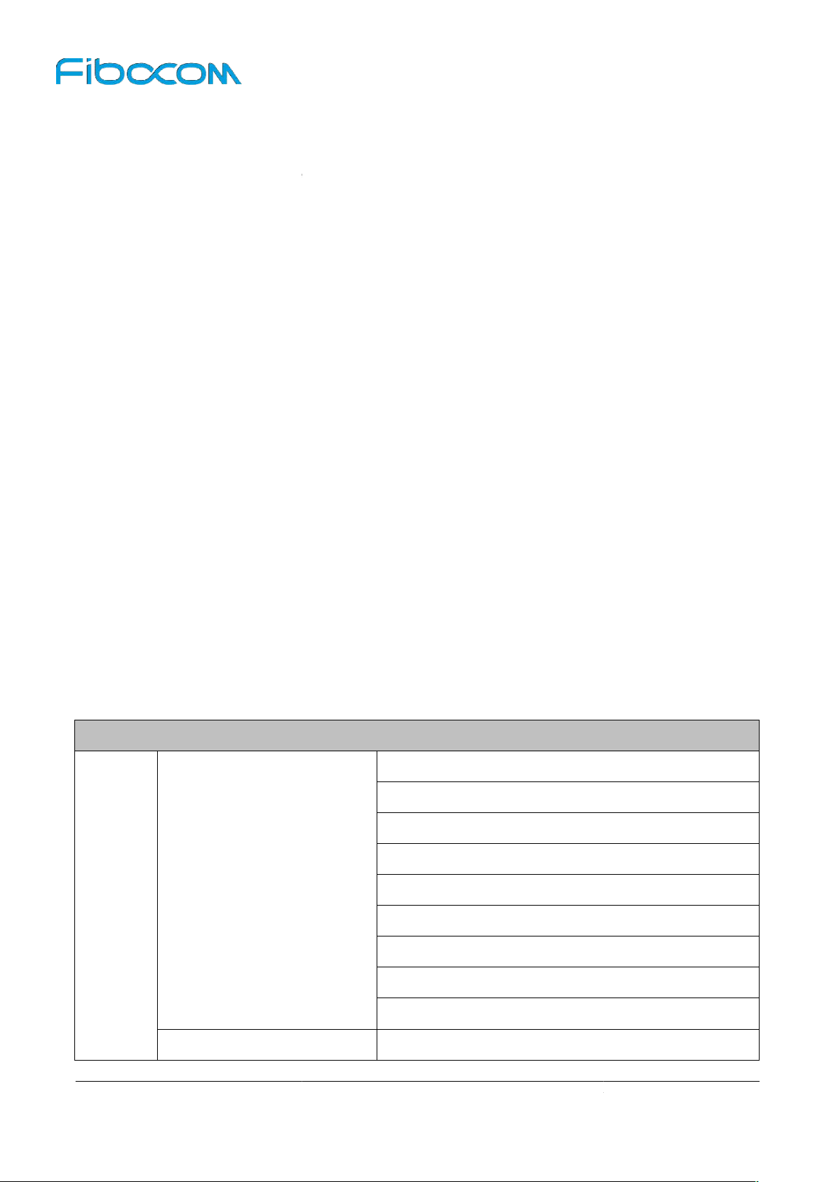
2.4
CA
s
CA Combinations
2CA
Inter-band
1+3,5,18,19,20,21,26
2+4,5,12,13,17,29,30,66
3+5,7,8,19,20,28
4+5,12,13,17,29,30
5+7,30,66
7+20,28
12+30
13+66
Intra-band
L850-GL Hardware User Manual
29+30
2,3,4,7,40,41
ritten authorization -
Page 13 of 51
Page 14
Reproduction forbidden without Fibocom Wireless Inc. w
2 contiguous plus inter
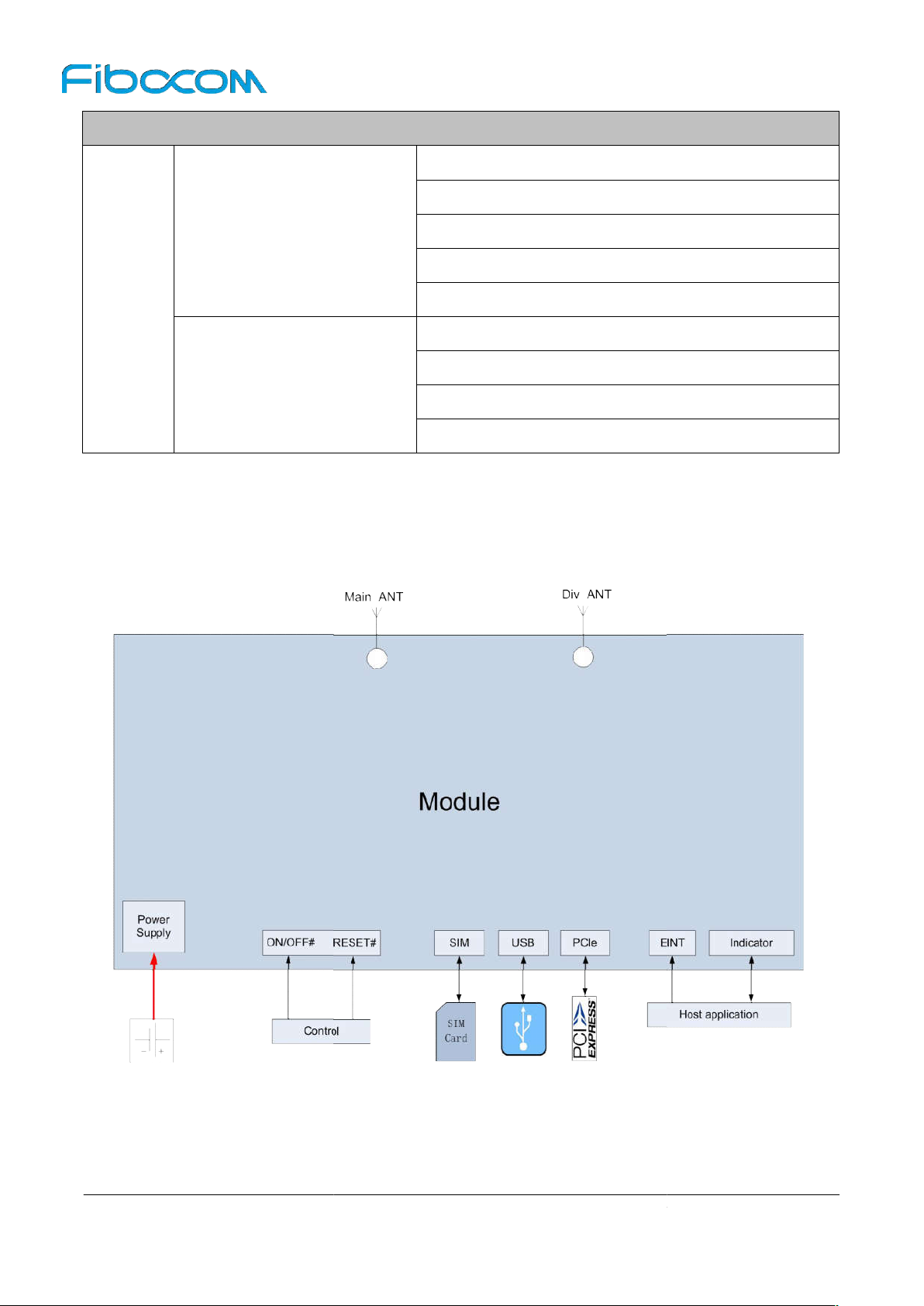
Framework
The peripheralapplicationsfor L850 module are shown in Figure 2
All Rights Reserved.
1+19+21
2+4+5, 2+4+13, 2+5+30, 2+12+30, 2+29+30
5+66+66, 13+66+66, 66+66+2, 66+66+66
CA Combinations
Inter-band
1+3+7, 1+3+19, 1+3+20,
3+7+20, 3+7+28
4+5+30, 4+12+30, 4+29+30
5+66+2, 13+66+2
2+2+5, 2+2+13
3+3+7, 3+7+7, 3+3+20
4+4+5, 4+4+13
3CA
2.5
Application
-band
-1:
L850-GL Hardware User Manual
Figure2-1 Application Framework
ritten authorization -
Page 14 of 51
Page 15
Reproduction forbidden without Fibocom Wireless Inc. w
Framework
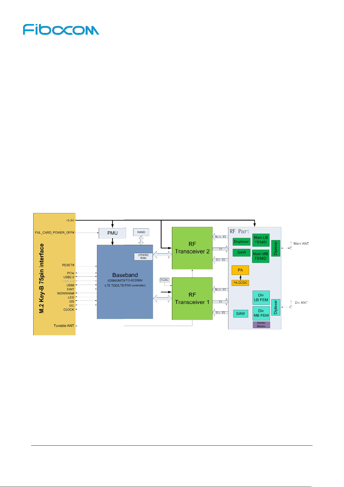
The hardware framework in Figure 2
GSM/UMTS/LTE FDD controller/Power supply
NAND/internal LPDDR2 RAM
Interface
The L850 module applies standard M.2 Key
All Rights Reserved.
2 shows the main hardware functions of L850 module,
2.6
Hardware
base band and RF functions.
-
including
Baseband contains the followings:
Application interface
RF contains the followings:
RF Transceiver
RF Power/PA
RF Front end
RF Filter
Antenna
3 Application
3.1
M.2Interface
L850-GL Hardware User Manual
Figure 2-2 Hardware Framework
-B interface, with a total of 75 pins.
ritten authorization -
Page 15 of 51
Page 16
Reproduction forbidden without Fibocom Wireless Inc. w
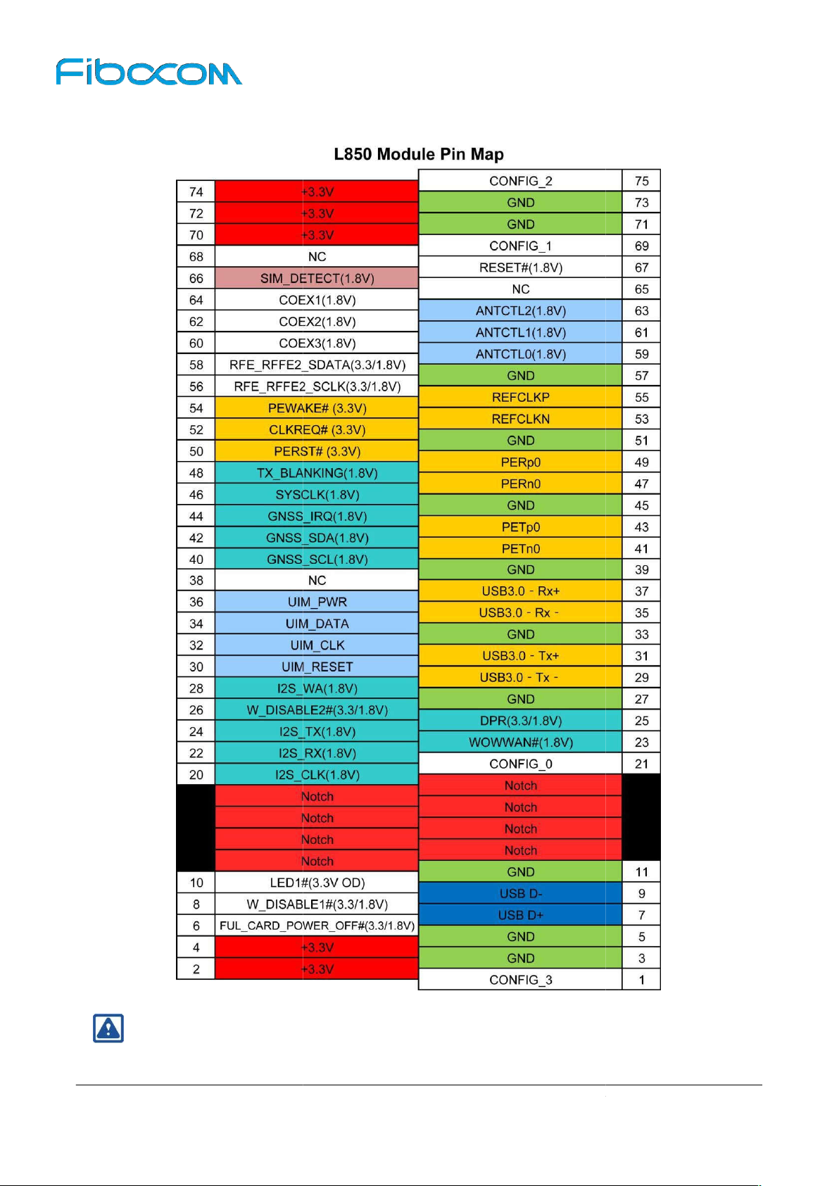
Pin “Notch” represents the gap of t
All Rights Reserved.
3.1.1
Pin Distribution
Note:
L850-GL Hardware User Manual
Figure 3-1 Pin Distribution
he gold fingers.
ritten authorization -
Page 16 of 51
Page 17
Reproduction forbidden without Fibocom Wireless Inc. w
Reset Value
NC
PU
PD
PD
GND
PD
All Rights Reserved.
NC,L850 M.2 module is configured as
PCIe,USB3.0 interface
power
GND,L850 M.2 module is configured as
PCIe,USB3.0 interface
on
open
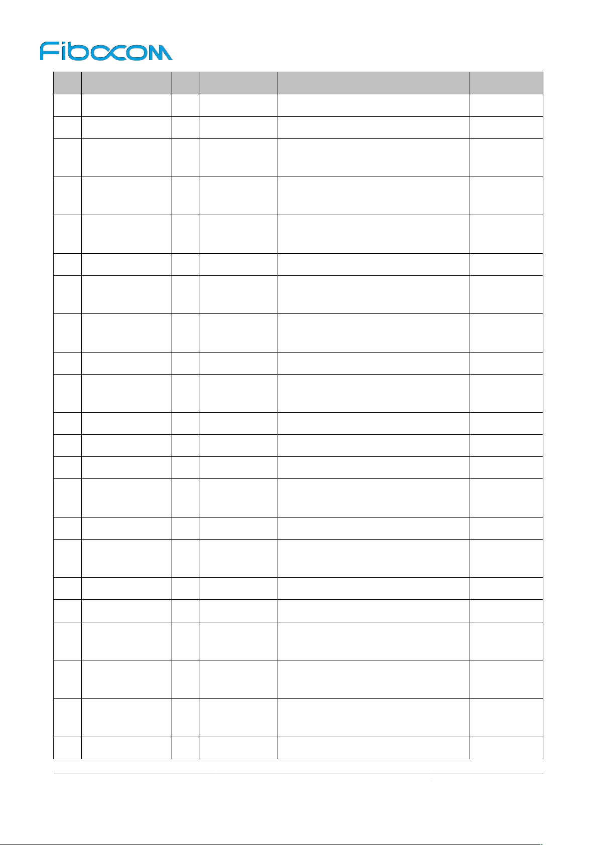
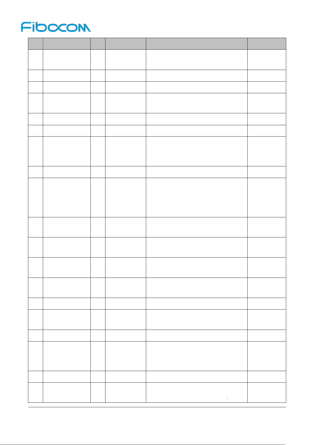
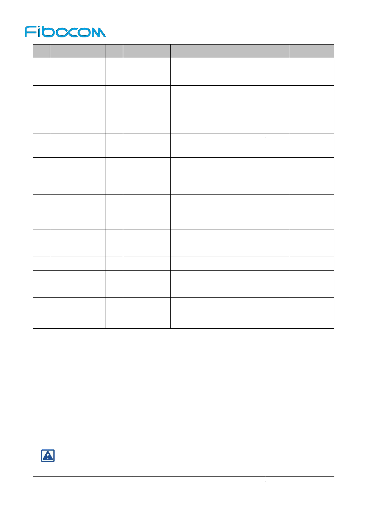
3.1.2
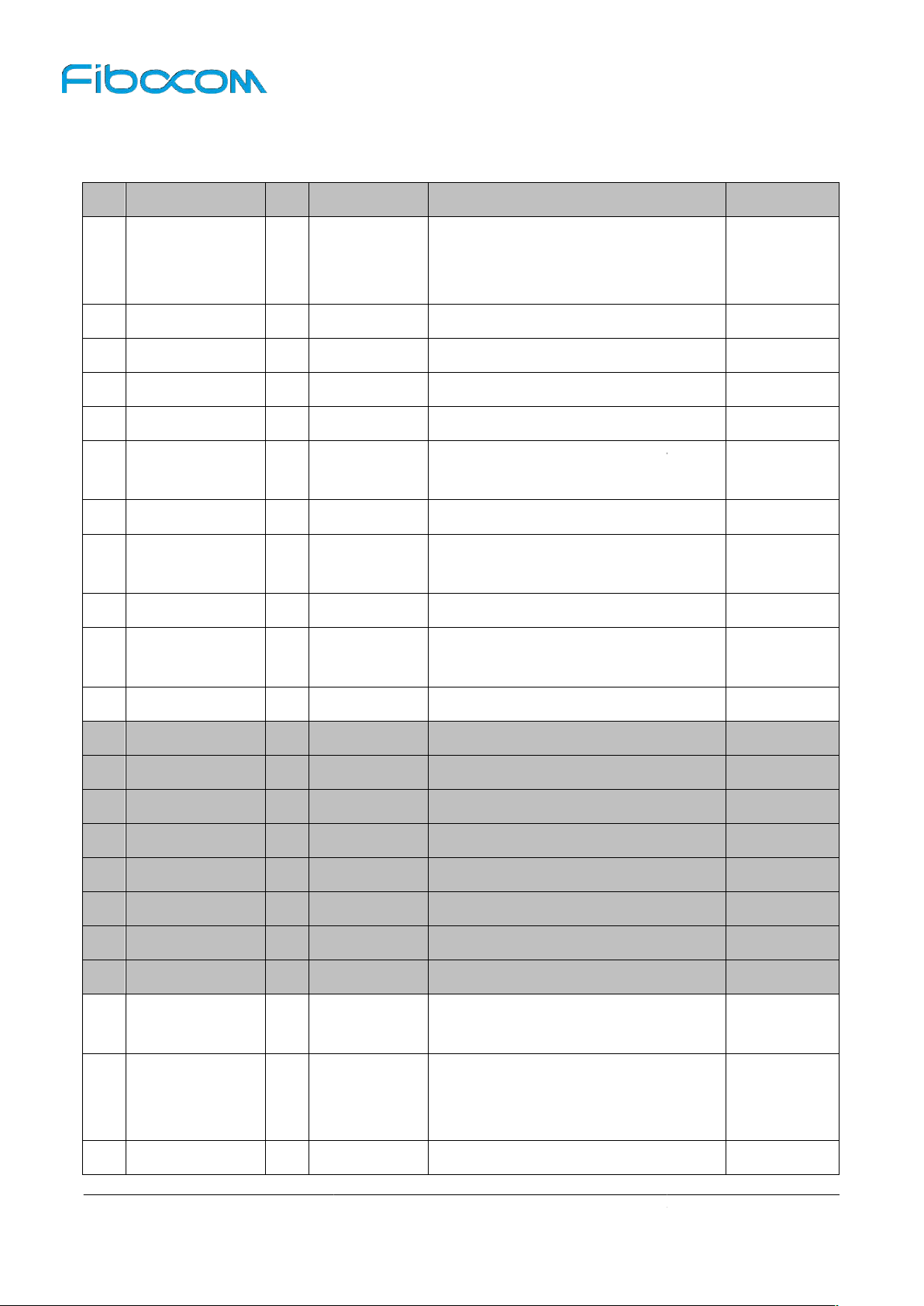
The pin definition is as follows:
Pin Pin Name I/O
1
2
3
4
5
6
7
Pin Definition
CONFIG_3
+3.3V PI
GND
+3.3V PI
GND
FUL_CARD_
POWER_OFF#
USB D+ I/O
O
I
8
W_DISABLE1# I
Pin Description
the WWAN –
type
Power input
GND
Power input
GND
Power enable,Module
input,internal pull up
USB Data Plus
WWAN Disable,active low
Type
Power Supply
Power Supply
Power Supply
Power Supply
CMOS
3.3/1.8V
0.3---3V
CMOS
3.3/1.8V
9
USB D- I/O
10 LED1#
11 GND
12 Notch
13 Notch
14 Notch
15 Notch
16 Notch
17 Notch
18 Notch
19 Notch
20 I2S_CLK
O
T
O
USB Data Minus
System status LED,Output
drain,CMOS 3.3V
GND
Notch
Notch
Notch
Notch
Notch
Notch
Notch
Notch
I2S Serial clock,
Reserved
0.3---3V
CMOS 3.3V
Power Supply
CMOS 1.8V
21 CONFIG_0
22 I2S_RX
L850-GL Hardware User Manual
I
I2S Serial receive data,
the WWAN –
type
CMOS 1.8V
ritten authorization -
Page 17 of 51
Page 18
Reproduction forbidden without Fibocom Wireless Inc. w
Reset Value
PD
PD
PU
PU
PD
PU
PU
All Rights Reserved.
PCIe TX Differential signals Positive
Pin Pin Name I/O
23 WOWWAN#
24 I2S_TX
25 DPR
O
O
I
26 W_DISABLE2# I
27 GND
28 I2S_WA
USB3.0‐Tx‐
29
30 UIM_RESET
USB3.0‐Tx+
31
O
O
O
O
Pin Description
Reserved
Wake up host
L
I2S Serial transmit data,
Reserved
Body SAR Detect,active low
GNSS disable,active low,
Reserved
GND
I2S Word alignment/select,
Reserved
USB3.0 Transmit data minus,
Not support now
SIM reset signal
USB3.0 Transmit data plus,
Not support now
Type
CMOS 1.8V
CMOS 1.8V
CMOS
3.3/1.8V
CMOS
3.3/1.8V
Power Supply
CMOS 1.8V
1.8V/3V
32 UIM_CLK
33 GND
34 UIM_DATA I/O
USB3.0‐Rx‐
35
36 UIM_PWR
USB3.0‐Rx+
37
38 NC
39 GND
40 GNSS_SCL
41 PETn0
42 GNSS_SDA
O
I
O
I
O
O
I/O
L
L
SIM clock Signal
GND
SIM data input/output
USB3.0 receive data minus,
Not support now
SIM power supply,3V/1.8V
USB3.0 receive data plus,
Not support now
NC
GND
I2C Serial clock,
Reserved
PCIe TX Differential signals
Negative
I2C Serial data input/output,
Reserved
1.8V/3V
Power Supply
1.8V/3V
1.8V/3V
Power Supply
CMOS 1.8V
CMOS 1.8V
43 PETp0
L850-GL Hardware User Manual
O
ritten authorization -
Page 18 of 51
Page 19
Reproduction forbidden without Fibocom Wireless Inc. w
Reset Value
PD
PD
PD
PD
All Rights Reserved.
Differential signals Positive
Reset is a functional reset to the
In card as defined by the PCIe Mini
Clock Request is a reference clock
signal as defined by the PCIe
Mini Card CEM specification; Also used
PCIe PME Wake. Open Drain with pull
Wireless Coexistence between WWAN
and WiFi/BT modules. IDC_UART_TXD,
between WWAN
IDC_UART_RXD
Pin Pin Name I/O
44 GNSS_IRQ
45 GND
46 SYSCLK
47 PERn0
48 TX_BLANKING
49 PERp0
50 PERST#
51 GND
52
CLKREQ#
I
O
I
O
I
I
O
Pin Description
26M clock output
PA Blanking Timer
T
GNSS Interrupt Request,
Reserved
GND
PCIe RX Differential signals
Negative
PCIe RX
PEAddCard CEM specification
GND
T
request
Type
CMOS 1.8V
Power Supply
1.8V
CMOS 1.8V
CMOS 3.3V
Power Supply
CMOS 3.3V
53 REFCLKN
54 PEWAKE#
55 REFCLKP
RFE_RFFE2_
56
SCLK
57 GND
RFE_RFFE2_
58
SDATA
59 ANTCTL0
60 COEX3
I
O
L
I
O
O
O
O
by L1 PM Substates
PCIe Reference Clock signal
Negative
up on platform,active low
PCIe Reference Clock signal
Positive
MIPI Interface Tunable ANT,
RFFE2 clock,Open Drain output
GND
MIPI Interface Tunable ANT,
RFFE2 data,Open Drain output
Tunable ANT CTRL0
Reserved
CMOS 3.3V
CMOS
3.3/1.8V
Power Supply
CMOS
3.3/1.8V
CMOS 1.8V
CMOS
3.3/1.8V
61 ANTCTL1
62 COEX2
L850-GL Hardware User Manual
O
I
T
Tunable ANT CTRL1
Wireless Coexistence
and WiFi/BT modules,
ritten authorization -
CMOS 1.8V
CMOS 1.8V
Page 19 of 51
Page 20
Reproduction forbidden without Fibocom Wireless Inc. written authorization
Reset Value
PD
GND
GND
Reset Value: The initial status after modulereset, not the status when working.
The unused pins can be left floating.
All Rights Reserved.
Wireless Coexistence between WWAN
GNSS_EXT_FTA
SIM Detect,internal pull up(330KΩ),
input,internal
GND,L850 M.2 module is configured as
PCIe,USB3.0 interface
GND,L850 M.2 module is configured as
PCIe,USB3.0 interface
pull
Pin Pin Name I/O
63 ANTCTL2
64 COEX1
65 NC
66 SIM_DETECT
67 RESET#
68 NC
69 CONFIG_1
O
O
T
I
I
O
Pin Description
,Reserved
Tunable ANT CTRL2
Type
CMOS 1.8V
and WiFi/BT modules,
,Reserved
NC
active high
WWAN reset
up(10KΩ),active low
NC
the WWAN –
type
CMOS 1.8V
CMOS 1.8V
CMOS 1.8V
O
Power input
GND
Power input
GND
Power input
the WWAN –
type
70 +3.3V PI
71 GND
72 +3.3V PI
73 GND
74 +3.3V PI
75 CONFIG_2
H:High Voltage Level
L: Low Voltage Level
PD:Pull-Down
PU:Pull-Up
T:Tristate
OD:Open Drain
Power Supply
Power Supply
Power Supply
Power Supply
Power Supply
PP:Push-Pull
PI: Power Input
PO: Power Output
Note:
L850-GL Hardware User Manual
-
Page 20 of 51
Page 21
Reproduction forbidden without Fibocom Wireless Inc. written authorization
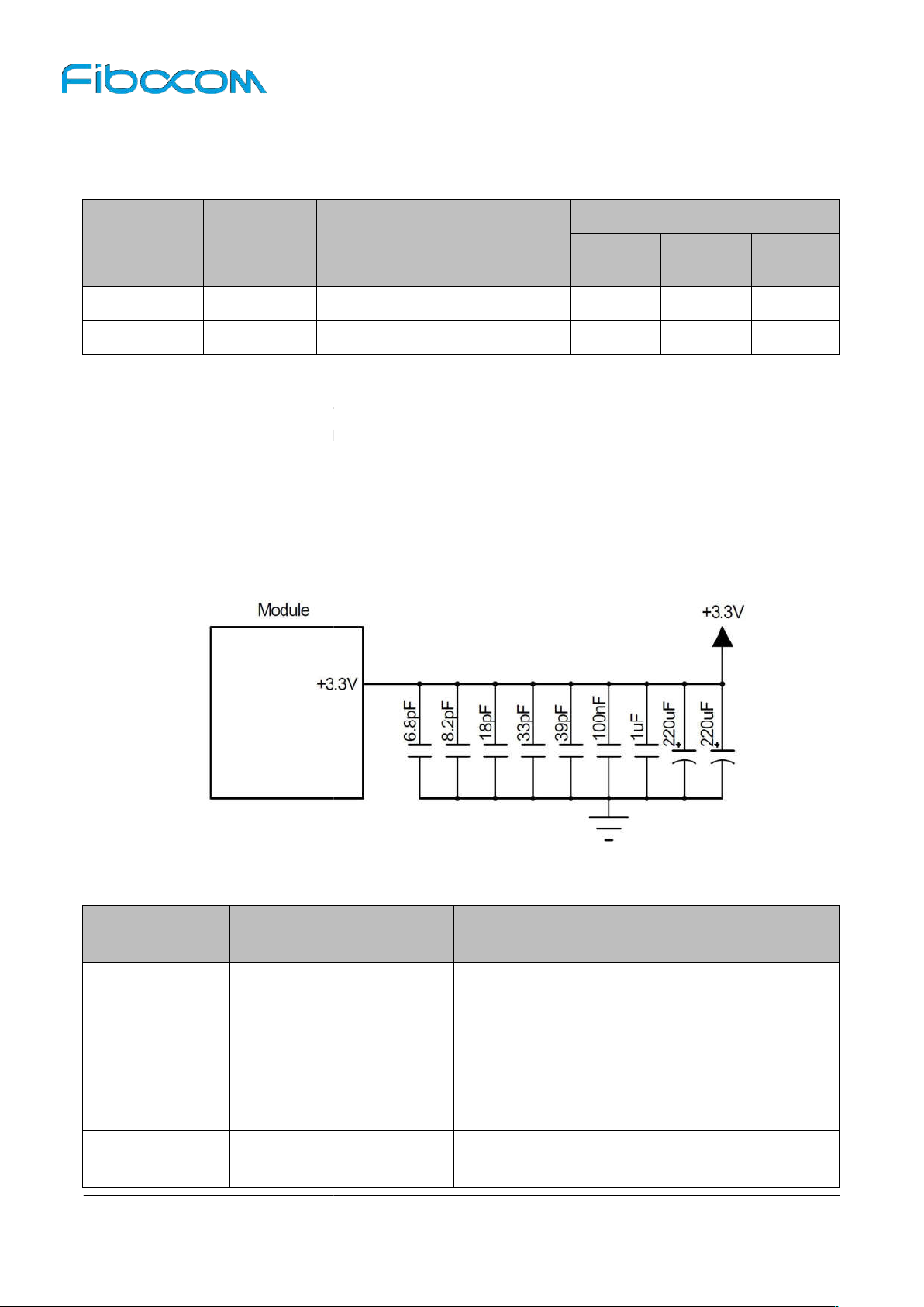
The power interface of L850 module as shown in the following table:
I/O
PI
PO
L850 module uses PCIe interface, according to the PCIe specification, the PCIe Vmain should be used as
the +3.3V power source, not the Vaux. The Vaux is the PCIe backup power source and
as the power supply. In addition, the DC/DC power supply other than PCIe ports should not be used as
the external power cannot control the module status through the PCIe protocol.
The L850 module should be powered through
The filter capacitor design for power supply as shown in the following
stabilizing
Digital signal noise
All Rights Reserved.
DC Parameter
Typical
Value
3.3
1.8V/3V
the +3.3V pins, and the power supply design is shown in
Reduce power fluctuations of the module in
operation, requiring capacitors with
LDO or DC/DC power supply requires the
capacitor of no less than
The capacitor for battery power supply can
Filter out the interference generated from the clock
3.2
Power Supply
(V)
Pin
2,4,70,72,74 +3.3V
36 UIM_PWR
3.2.1
Figure 3-2:
Power Supply
Pin Name
Pin Description
Power supply input 3.135
USIM power supply
Minimum
Value
4.4
Maximum
Value
it is not sufficient
Figure 3-2 Power Supply Design
Recommended
capacitance
220uF x 2
1uF,100nF
L850-GL Hardware User Manual
Application
Voltagecapacitors
table:
Description
reduced to 100~200uF
and digital signals
low ESR.
440uF
be
-
Page 21 of 51
Page 22
Reproduction forbidden without Fibocom Wireless Inc. written authorization
MHzfrequency band
1500/1700/1800/1900,2100/
2300,2500/2600MHzfrequen
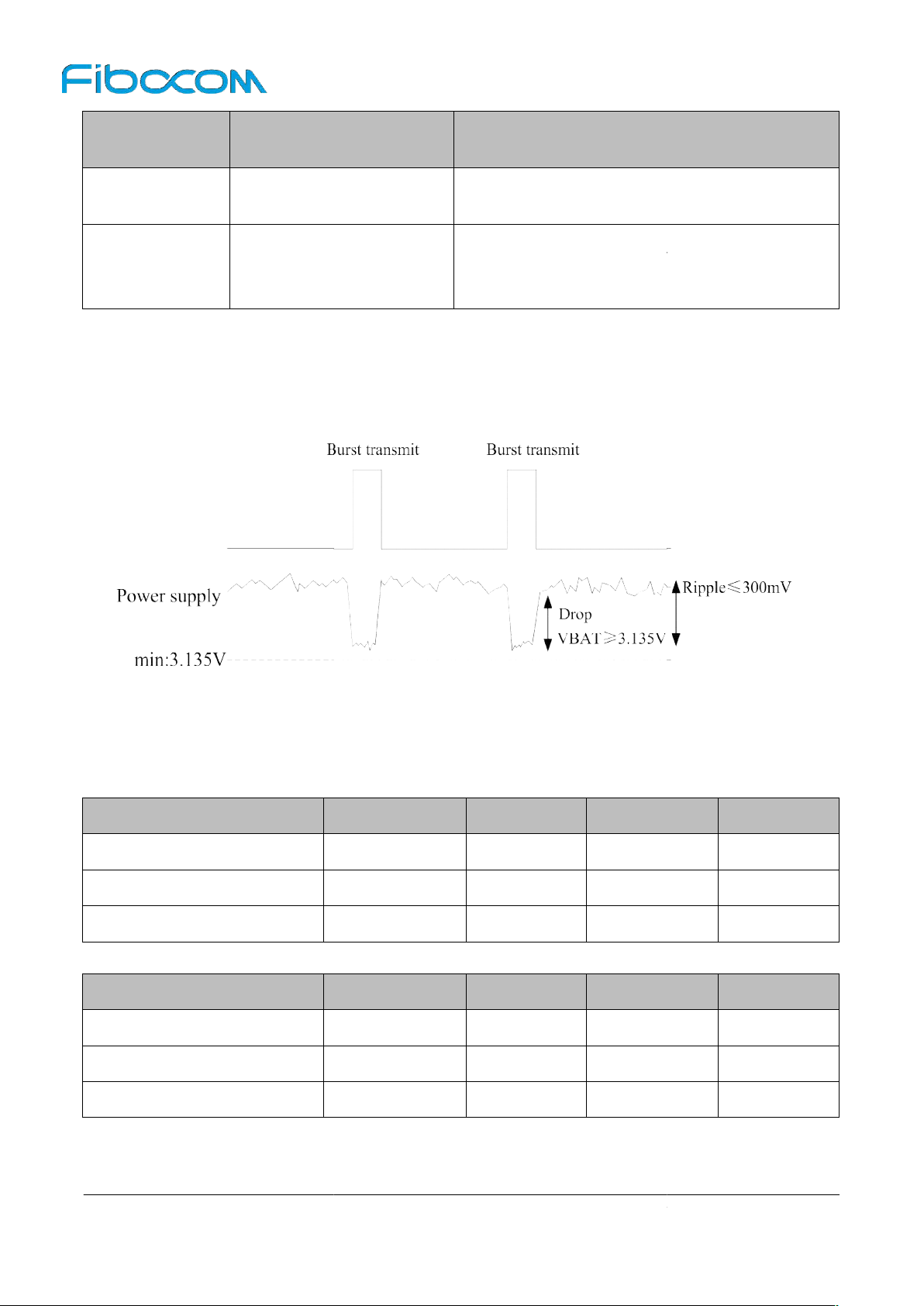
The stable power supply can ensure the normal operation of L850 module;and the ripple of the
supply should be less than 300mV in design. When the module operates with themaximum emission
power, the maximum operating current can reach 1000mA, so the power source should be not lower than
3.135V, or the module may shut down or reboot. The power
The L850module 1.8V logic level definitionas shown in the following table:
Minimum
1.71
1.3
-
The L850module 3.3V logic level definition as shown in the following table:
Minimum
3.135
2.3
-
All Rights Reserved.
band RF interference
frequency
supply limits are shown in Figure 3
Maximum
Maximum
Recommended
capacitance
39pF,33pF
18pF,8.2pF,6.8pF
Application
700/800,
cy band
850/900
Description
Filter out low frequency
Filter out
interference
medium/high
frequency
band
RF
Figure 3-3 Power Supply Limit
-3:
3.2.2
Logic level
power
Parameters
1.8V logic level
V
IH
V
IL
1.8 1.89
0.3
Typical
1.8 1.89
Parameters
3.3V logic level
V
IH
V
IL
L850-GL Hardware User Manual
3.3 3.465
0.3
Typical
3.3 3.465
0
0.5
0
0.9
Unit
V
V
V
Unit
V
V
V
-
Page 22 of 51
Page 23
Reproduction forbidden without Fibocom Wireless Inc. written authorization
Consumption
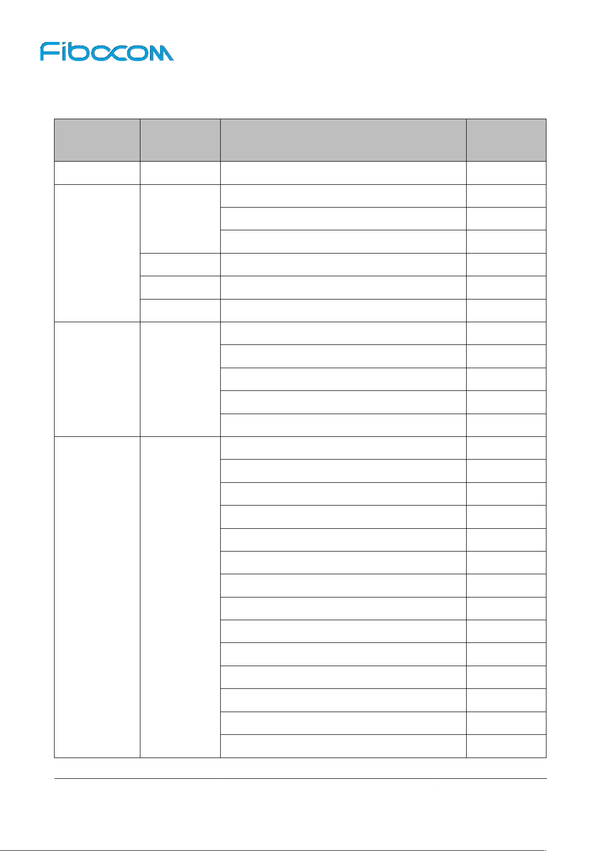
In the condition of 3.3V power supply, the L850 power consumption as shown in the following table:
All Rights Reserved.
Paging cycle #64 frames (0.64 sec DRx cycle)
Paging cycle #64 frames (0.64 sec DRx cycle)
3.2.3
Power
Parameter
Mode
Condition
Average
Current(mA)
I
off
Power off
WCDMA
Power supply,module power off
DRX=6
DRX=8
0.08
2.5
1.8
I
Sleep
I
WCDMA-RMS
DRX=9
LTE FDD
LTE TDD
Radio Off
AT+CFUN=4,Flight mode
WCDMA Data transfer Band 1 @+23.5dBm
WCDMA Data transfer Band 2 @+23.5dBm
WCDMA
WCDMA Data transfer Band 4 @+23.5dBm
1.6
2.6
2.8
1.2
680
710
500
I
LTE-RMS
WCDMA Data transfer Band 5 @+23.5dBm
WCDMA Data transfer Band 8 @+23.5dBm
LTE FDD Data transfer Band 1 @+23dBm
530
580
760
LTE FDD Data transfer Band 2 @+23dBm
760
LTE FDD Data transfer Band 3 @+23dBm
770
LTE FDD Data transfer Band 4 @+23dBm
LTE FDD Data transfer Band 5 @+23dBm
LTE FDD Data transfer Band 7 @+23dBm
710
550
TBD
LTE FDD
LTE FDD Data transfer Band 8 @+23dBm
LTE FDD Data transfer Band 11 @+23dBm
LTE FDD Data transfer Band 12 @+23dBm
LTE FDD Data transfer Band 13 @+23dBm
LTE FDD Data transfer Band 17 @+23dBm
540
TBD
600
560
580
LTE FDD Data transfer Band 18 @+23dBm
LTE FDD Data transfer Band 19 @+23dBm
LTE FDD Data transfer Band 20 @+23dBm
L850-GL Hardware User Manual
560
520
630
-
Page 23 of 51
Page 24
Reproduction forbidden without Fibocom Wireless Inc. written authorization
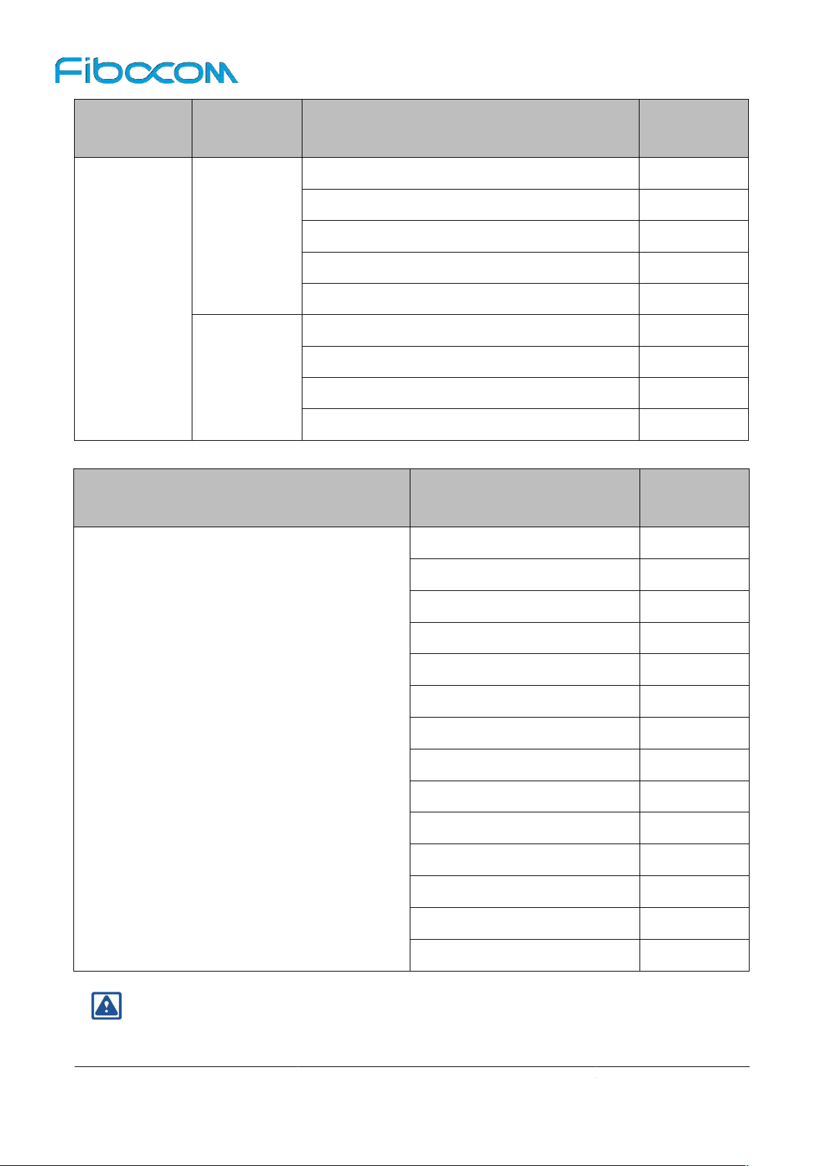
The power consumption of L850 in 3CA mode as shown in the following tables:
1+3+7, 1+3+19, 1+3+20, 1+19+21
2+4+13, 2+5+30, 2+12+30, 2+29+30
5+66+66, 13+66+66, 66+66+2, 66+66+66
average value obtained by testing some samples.
All Rights Reserved.
Parameter
Mode
Condition
Average
Current(mA)
LTE FDD Data transfer Band 21 @+23dBm
LTE FDD Data transfer Band 26 @+23dBm
LTE FDD Data transfer Band 28 @+23dBm
LTE FDD Data transfer Band 30 @+23dBm
LTE FDD Data transfer Band 66 @+23dBm
LTE TDD Data transfer Band 38 @+23dBm
LTE TDD Data transfer Band 39 @+23dBm
LTE TDD
LTE TDD Data transfer Band 40 @+23dBm
LTE TDD Data transfer Band 41 @+23dBm
Condition
3CA Combination
(LTE FDD 3CA, Full RB)
Band 1 @+22dBm
Band 2 @+22dBm
Band 3 @+22dBm
Band 4 @+22dBm
TBD
540
530
TBD
700
450
320
420
440
Average
Current(mA)
720
880
860
760
2+4+5,
3+7+20, 3+7+28
4+5+30, 4+12+30, 4+29+30
5+66+2, 13+66+2
2+2+5, 2+2+13
3+3+7, 3+7+7, 3+3+20
4+4+5, 4+4+13
Note:
The data above is an
L850-GL Hardware User Manual
Band 5 @+22dBm
Band 7 @+22dBm
Band 12 @+22dBm
Band 13 @+22dBm
Band 19 @+22dBm
Band 20 @+22dBm
Band 21 @+22dBm
Band 28 @+22dBm
Band 30 @+22dBm
Band 66 @+22dBm
-
800
1110
790
630
760
750
950
720
1330
710
Page 24 of 51
Page 25
Reproduction forbidden without Fibocom Wireless Inc. written authorization
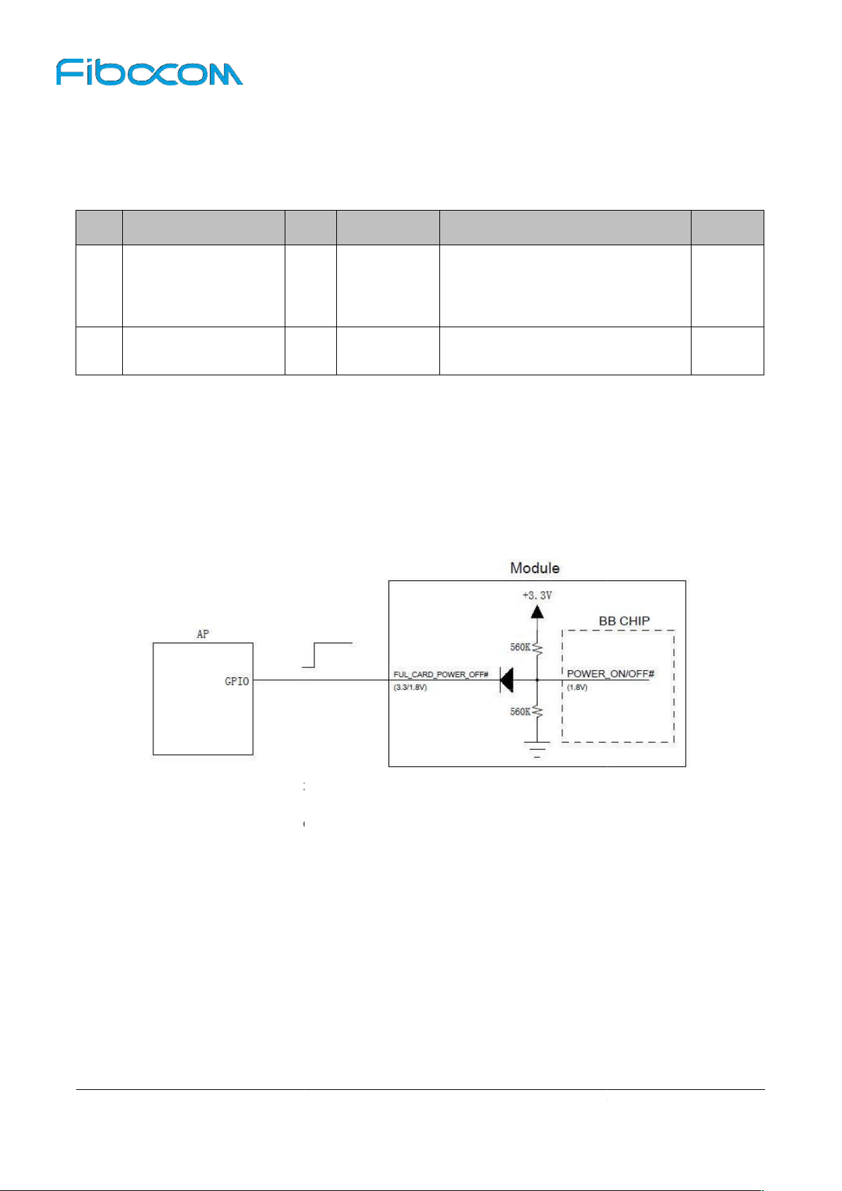
The L850 module provides two control signals for power on/off and reset operations, the pin defined as
FUL_CARD_POWER_OFF# pin needs an external 3.3V or 1.8V pull up for booting up. The
VDD_1V8 should be provided from the external circuit. AP (Application Processor) controls the module
and the circuit design is shown in Figure3
igure 3
Sequence
After powering on, the module will start
more than 20ms (100msis recommended). Meanwhile, the module will output 1.8V voltag
VSD2_1V8 pin and start the initialization process. The start
I/O
All Rights Reserved.
up Controlled by AP
up by pulling upthe FUL_CARD_POWER_OFF# signal for
up timing is shown in Figure 3
Power on/off signal,internalpull
High or floating: Power on
Reset signal, internal 10KΩ
3.3
Control Signal
shown in the following table:
Pin Pin Name
6
67 RESET#
FUL_CARD_POWER_
OFF#
Reset Value Functions
I
PU
I
-up
Low : Power off
pull-up,active low
Type
3.3/1.8V
1.8V
3.3.1
3.3.1.1
Module Start-Up
Start-upCircuit
The
start-up,
3.3.1.2
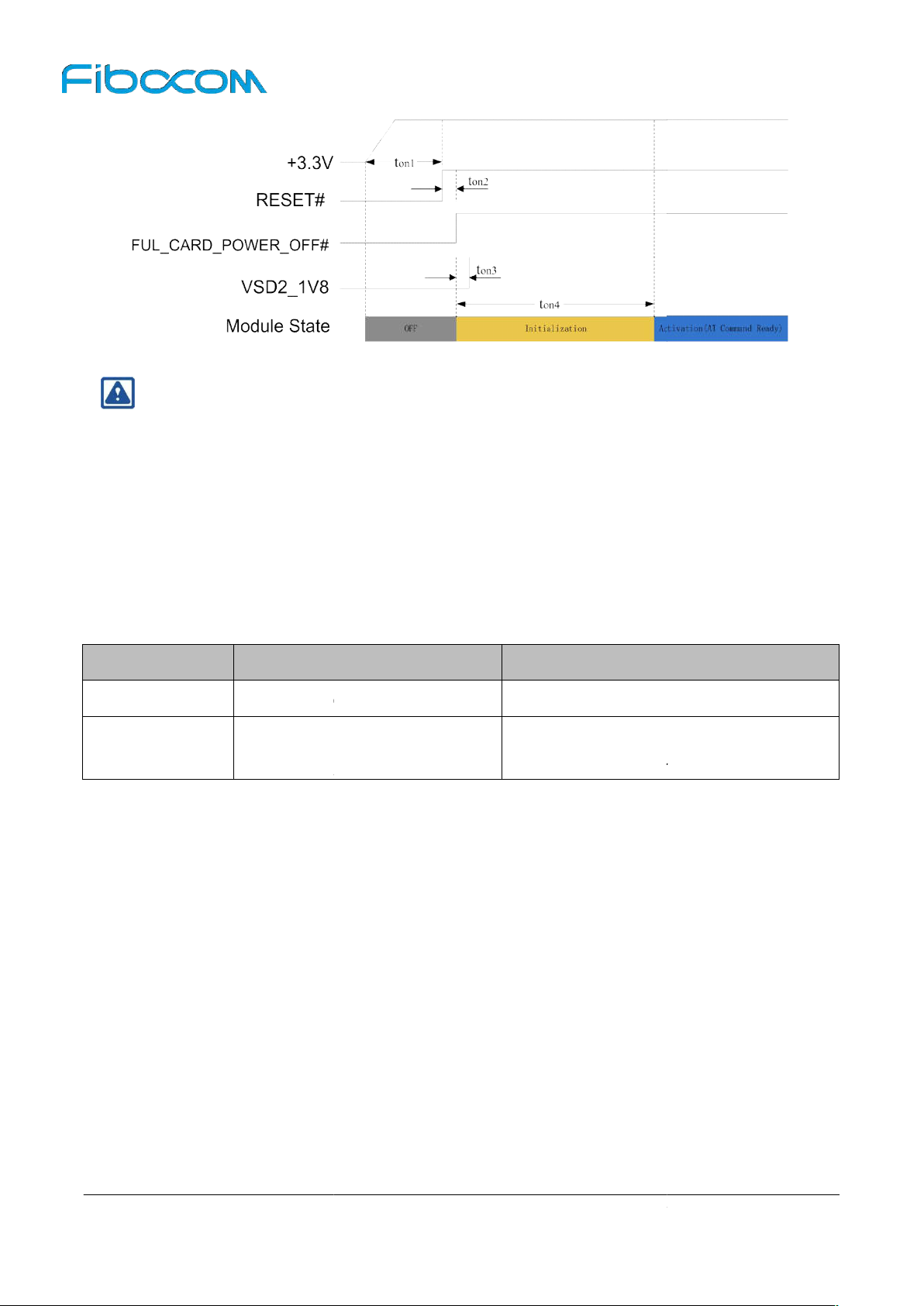
Start-upTiming
F
-4 Circuit for Module Start-
-4:
-
L850-GL Hardware User Manual
e through
-
-
-5:
Page 25 of 51
Page 26
Reproduction forbidden without Fibocom Wireless Inc. written authorization
The VSD2_1V8 signal is the internal PMU 1.8V output voltage which is not connected
interface. The above timing of VSD2_1V8 is only for reference.
The RESET# is required to pull high with a t
tocharge thecapacitors for +3.3V power supply. If the +3.3V power supply is already
before starting upthe module, the delay time can be ignored.
Shutdown
The module can be shut down by the following controls:
Sending AT+CPWROFF command
FUL_CARD_POWER_OFF# pin
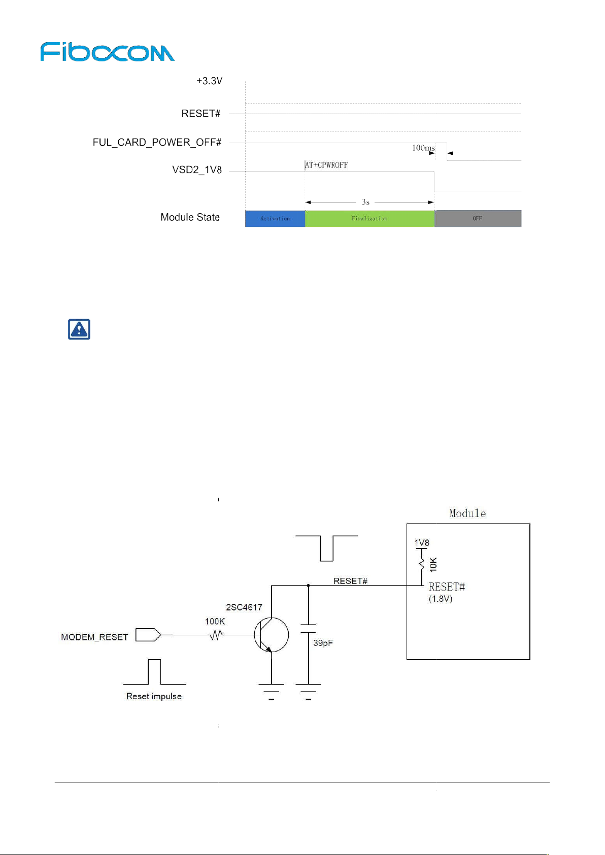
The module can be shut downby sending AT+CPWROFF command. When the module receives the
software shutdown command, the module will start the finalization process (the reverse process of
initialization), andit will be completed after 3s. In the finalization
SIM card and some other parameters from memory, then clear the memory and PMU will be powered off.
After shutdown, the VSD2_1V8 voltage is also shut down. The software control timing isshown in Figure
All Rights Reserved.
delay after the +3.3V, because it takes some time
recommend
Only used whena hardware exception occurs
and the software control cannot be used.
Figure 3-5 Timing Control for Start-up
Note:
3.3.2
Module
Shutdown Control Action
Software
Pull down
Hardware
on1
Condition
Normal shutdown(
to the M.2
stable
)
3-6:
L850-GL Hardware User Manual
-
Page 26 of 51
Page 27
Reproduction forbidden without Fibocom Wireless Inc. written authorization
Figure 3
After the software shutdown, the FUL_CARD_POWER_OFF # pin will remain high which prevents the
module from restarting again. Toenable the next restart, the FUL_CARD_POWER_OFF#pin should be
The VSD2_1V8 signal is the internal PMU 1.8V output voltage which is not connected to the M.2
interface. The above timing of VSD2_1V8 is only for reference.
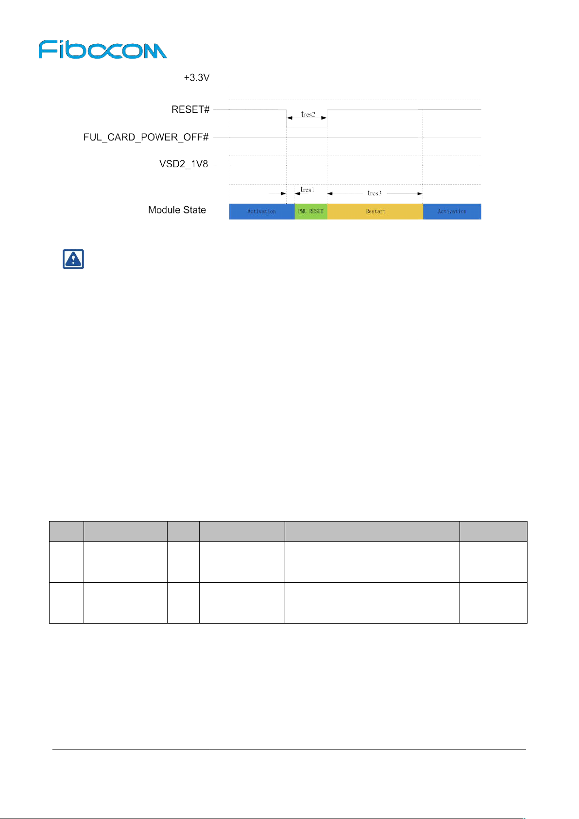
The L850 module can reset to its initial
(100msis recommended), and the module will restart after the RESET# signal is released. When the
customer executes RESET# function, the PMU remains its power inside the module. The recommended
cuit design is shown in the Figure 3
Figure 3
The reset control timing is shown in Figure 3
All Rights Reserved.
pulled low after shutting down.
Note:
-6 Software Shutdown Timing Control
3.3.3
cir
Module Reset
-7:
-7 Recommended Design for Reset Circuit
L850-GL Hardware User Manual
-8:
-
Page 27 of 51
Page 28
Reproduction forbidden without Fibocom Wireless Inc. written authorization
RESET# is a sensitive signal, it’s
case of PCB layout, the RESET# signal lines should keep away from the RF interference and
protected by GND. Also, the RESET# signal lines shall neither near the PCB edge nor route on
planes to avoid module from reset caused by ESD problems.
The L850 module supports USB2.0 which is compatible with USB High
Speed (12 Mbit/s). For the USB timing and electrical specification of L850 module,
to“Universal Serial Bus Specification 2.0”.
Definition
Reset Value
Application
USB interface is used for debugging only, so it only needs to introduce the USB interface test in hardware
All Rights Reserved.
Speed (480 Mbit/s) and USB Full
Figure 3-10 Reset Timing Control
Note:
the surface
3.4 USB Interface
USB interface just for debugging.
-
-
please refer
3.4.1
Pin# Pin Name I/O
7
9
3.4.2
design.
L850-GL Hardware User Manual
USB Interface
USB_D+
USB_D-
I/O
I/O
USB2.0 Interface
Description
USB Data Plus
USB Data Minus
Type
0.3---3V,
USB2.0
0.3---3V,
USB2.0
-
Page 28 of 51
Page 29
Reproduction forbidden without Fibocom Wireless Inc. written authorization
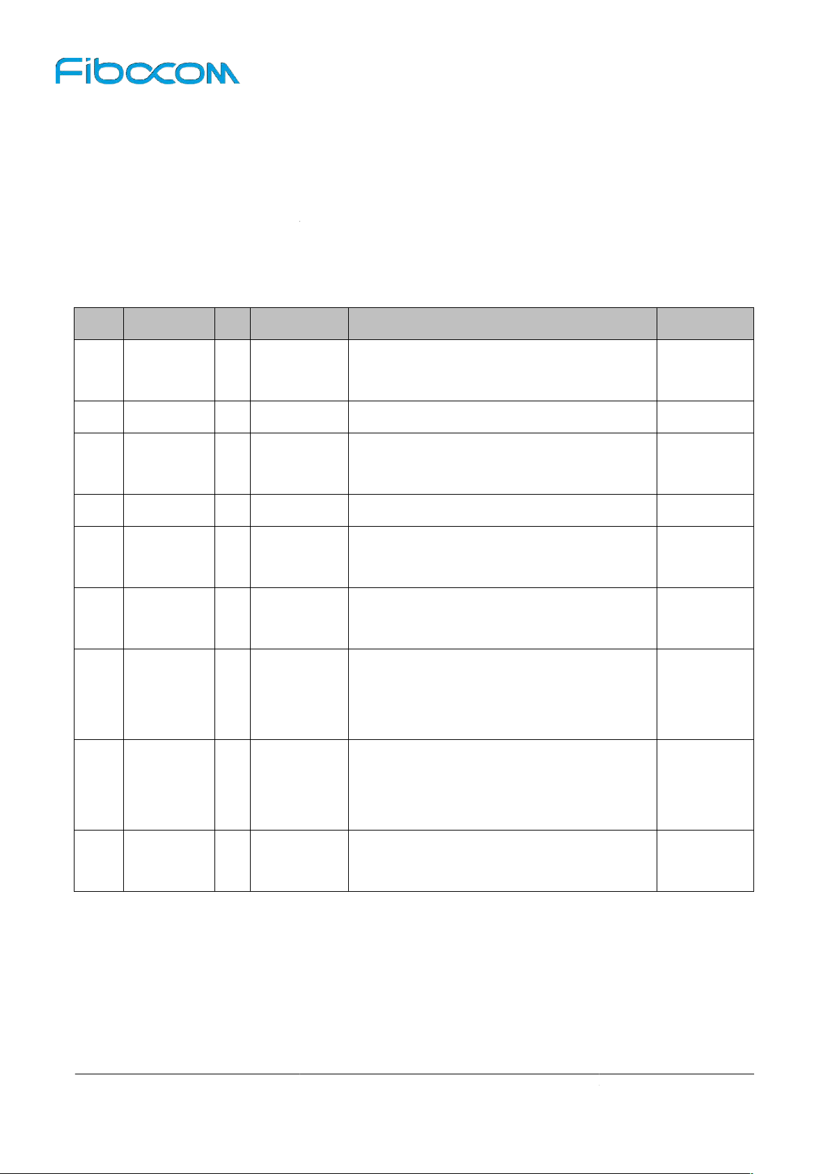
L850 module supports PCIe 1.0 interface and one data
After L850 module is inserted into PC, PCIe interface can, work with the drive program, map an MBIM
port and a GNSS port in Win10 system. While MBIM interface is used for initiating data service in Win10
receiving GNSS
Definition
Reset Value
Application
The reference circuit is shown in Figure 3
All Rights Reserved.
Reset is a functional reset to the Add
defined by the PCIe Mini Card CEM
Clock Request is a reference clock request
signal as defined by the PCIe Mini Card CEM
specification; Also used by L1 PM Substates
Wake. Open Drain with pull up on
In
3.5
PCIe Interface
transmission channel.
system and GNSS interface for
3.5.1
Pin# Pin Name I/O
41
43 PETP0
47
49 PERP0
53
55
PCIe Interface
PETn0
PERn0
REFCLKN I
REFCLKP I
O
O
I
I
data.
Description
PCIe TX Differential signals
Negative
PCIe TX Differential signals Positive
PCIe RX Differential signals
NegativeBit0
PCIe RX Differential signals Positive
PCIe Reference Clock signal
Negative
PCIe Reference Clock signal
Positive
Type
50
52
54
PERST#
CLKREQ#
PEWAKE# O
I
O
L
T
T
3.5.2
PCIe Interface
PE-
card as
specification
PCIe PME
platform,active low
-9:
CMOS 3.3V
CMOS 3.3V
CMOS 3.3V
L850-GL Hardware User Manual
-
Page 29 of 51
Page 30
Reproduction forbidden without Fibocom Wireless I
Figure 3
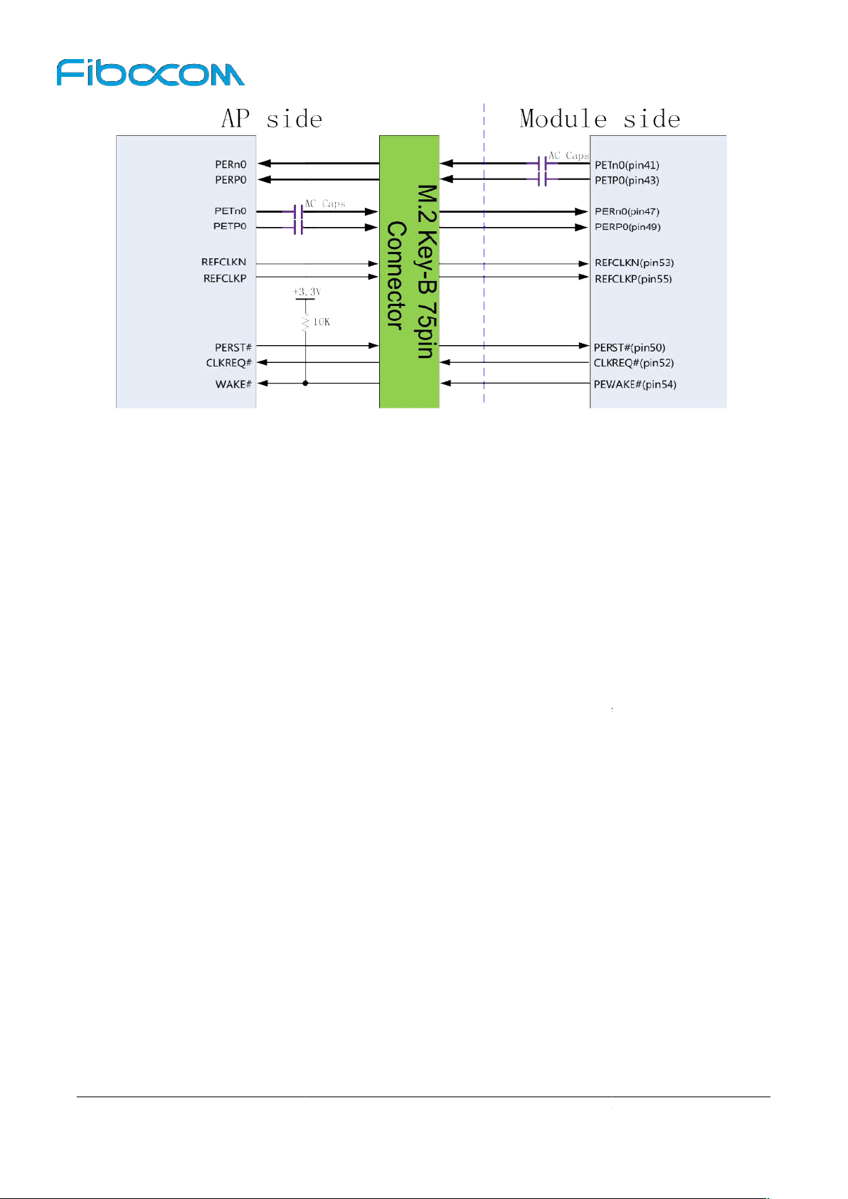
L850 module supports one PCIe 1.0 interface,
receiving pair RXP/N and clock pair CLKP/N.
PCIe can achieve the maximum transmission rate of 2.5 GT/s, and must strictly follow the rules below in
The differential signal pair lines shall
The differential signal pair lines shall be short if possible and be controlled within 500mm for AP end;
The impedance of differential signal pair lines is recommended to be 100 ohm, and can be
120 ohm i
It shall avoid the discontinuous reference ground, such as segment and space;
When the differential signal lines go through different layers, the via hole of grounding signal should
be in close to that of signal, and gene
holes and the lines shall never cross the segment of plane;
Try to avoid bended lines and avoid introducing common
influence the signal integrity and EMI of
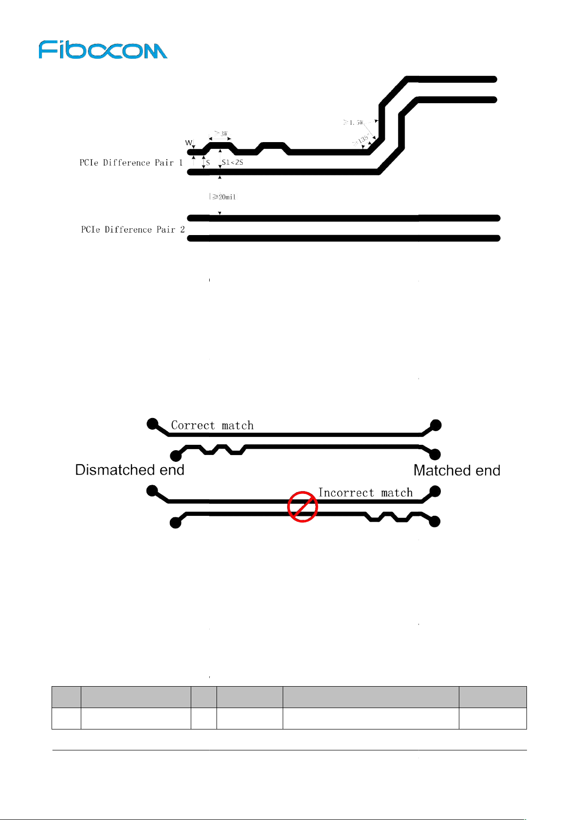
angle of all lines should be equal or greater than 135
lines should be larger than 20mil, and the line caused by bending should be greater than 1.5
times line width at least. When a serpentine line is used for length match with another line, the
bended length of each segment shall be at least 3 times the line
spacing between the bended part of the serpentine line and another one of the differential lines
must be less than 2 times the spacing of normal differential lines (S1<2S);
All Rights Reserved.
mode noise in the system, which will
, the spacing between difference pair
-9 Reference Circuit for PCIe Interface
PCB Layout:
controlled to 80~
be parallel and equal in length;
n accordance with PCIe protocol;
-3 grounding signal via
-
-10, the bending
L850-GL Hardware User Manual
°
nc. written authorization -
≥ 3W). The largest
Page 30 of 51
Page 31
Reproduction forbidden without Fibocom Wireless I
The difference in length of two data lines in difference pair should be within
match is required for all parts. When the length match is conducted for the differential lines, the
designed position of correct match should be close to that of incorrect match, as shown in Figure
11. However, there is no specific r
pair, that is, the length match is only required in the internal differential lines rather than between
different difference pairs. The length match should be close to the signal pin and pass
-
in USIM card interface, which supports 1.8V and 3V SIM cards.
The USIM pins descriptionas shown in the
I/O
PO
All Rights Reserved.
5mil, and the length
Figure 3-10 Requirement of PCIe Line
3-
small-angle bending design.
3.6
USIMInterface
Figure 3
the
The L850 module has a built-
3.6.1
Pin Pin Name
36 UIM_PWR
L850-GL Hardware User Manual
USIM Pins
following table:
Reset Value Description
USIM power supply
nc. written authorization -
Type
1.8V/3V
Page 31 of 51
Page 32
Reproduction forbidden without Fibocom Wireless I
I/O
I/O
Circuit
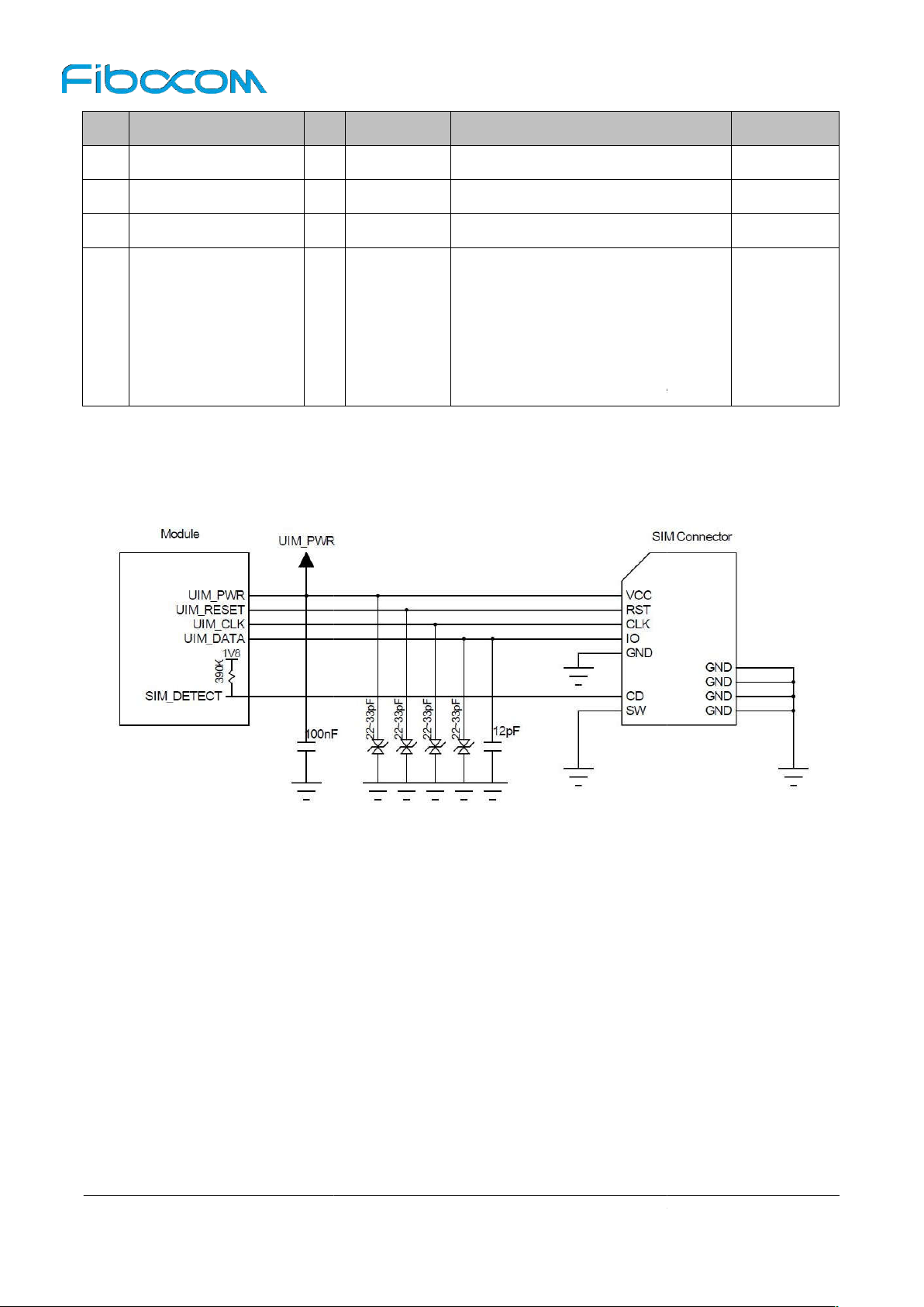
The reference circuit design for N.C. (Normally Closed)SIM card slot is shown in Figure 3
Figure 3
The principlesof theN.C.SIM card slot are described as follows:
is detached, it connects the short circuit between CD and SW pins, and drives the
When the SIM card is inserted, it connects an open circuit between CD and SW pins, and drives the
circuit design for N.O. (Normally Open) SIM card slot is shown in Figure 3
All Rights Reserved.
USIM data,internal pull up(4.7KΩ)
USIM card detect, internal 390K
Active high, and high level indicates
SIM card is inserted; and low level
indicates SIM card is detached.
Pin Pin Name
Reset Value Description
Type
30 UIM_RESET
32 UIM_CLK
34 UIM_DATA
66
SIM_DETECT
3.6.2
3.6.2.1
USIM Interface
N.C. SIMCard Slot
O
O
I
L
USIM reset
L
USIM clock
L
pull-up.
PD
1.8V/3V
1.8V/3V
1.8V/3V
1.8V
-12:
When the SIM card
SIM_DETECT pin low.
SIM_DETECT pin high.
3.6.2.2
N.O. SIM Card Slot
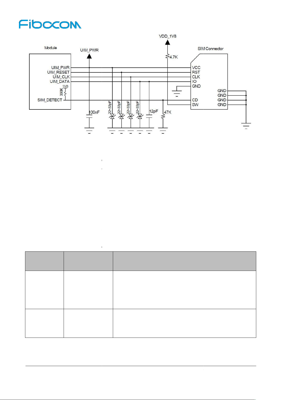
The reference
L850-GL Hardware User Manual
-12Reference Circuit for N.C. SIM Card Slot
-13:
nc. written authorization -
Page 32 of 51
Page 33
Reproduction forbidden without Fibocom Wireless I
13
The principlesof theN.O.SIM card slot are described as
When the SIM card is detached, it con
the SIM_DETECT pin low.
inserted,
Plugging
The L850 module supports the SIM
inserted or detached by detecting the SIM_DETECT pin state of the SIM card slot.
plugging function can be configuredby “AT+MSMPD” command, and the description for
AT command as shown in the following table:
plugging detection functionis enabled, the module detects that the SIM card is
insertedwhen the SIM_DETECT pin is high, then executes the initialization program and finish the
All Rights Reserved.
plugging function, which determines whether the SIM card is
plugging detection function is
The module can detect whether the SIM card is inserted or not
plugging detect function is disabled.
when starting up, and the
SIM_DETECT status will not be detected.
Figure 3-
When the SIM card is
SIM_DETECT pin high.
Reference Circuit for N.O. SIM Card Slot
follows:
it connects the short circuit between CD and
3.6.3
The SIM card hot-
AT Command
AT+MSMPD=1
AT+MSMPD=0
USIM Hot-
Hot-plugging
Detection
Enable
Disable
card hot-
Function Description
Default value, the SIM card hot-
enabled.
through the SIM_DETECT pin state.
The SIM card hot-
The module readsthe SIM card
SW pins, and drives the
After the SIM card hot-
L850-GL Hardware User Manual
nc. written authorization -
Page 33 of 51
Page 34

Reproduction forbidden without Fibocom Wireless I
network registration after reading the SIM ca
module determines that the SIM card is detachedand does not read the SIM card.
By default, SIM_DETECT is active
command. Please refer to the
The SIM card circuit design shall meet the EMC standards and ESD requirements with the
improvedcapability to resist interference, to ensure that the SIM card can work stably. Thefollowing
be noted in case of design:
The SIM card slotplacement should near the module as close as possible, and away from the RF
antenna, DC/DC power supply, clock signal lines, and other strong interference sources.
The SIM card slot with a metal shielding
The trace length between the SIM card slotand the module should not exceed 100mm, or it could
The UIM_CLK and UIM_DATA signal lines should be isolated by GND to avoid crosstalk
interference. If it is difficult for the layout, the whole SIM signal lines should be wrapped with
The filter capacitors and ESDdevices for SIM card signals should be placed near to the SIM card
slot, and the ESD devices with 22~
Indicator
The L850 module providesthree signals to indicate the operating status of the module, and the status
indicator pinsas shown in the following table:
Reset Value
All Rights Reserved.
high, which can be switched to active
interference ability.
output, externalGPS control
Note:
-
-low by the AT
3.6.4
guidelines should
USIM Design
reduce the signal quality.
housing can improve the anti-
GND as a group at least.
33pF capacitance should be used.
3.7
Status
Pin Pin Name
10 LED1#
23 WOWWAN#
48 TX_BLANKING
I/O
O
O
O
PD
PU
PD
Pin Description
System status LED, drain output.
Module wakes upHost (AP).
PA Blanking
signal.
Type
CMOS 3.3V
CMOS 1.8V
CMOS 1.8V
L850-GL Hardware User Manual
nc. written authorization -
Page 34 of 51
Page 35
Reproduction forbidden without Fibocom Wireless I
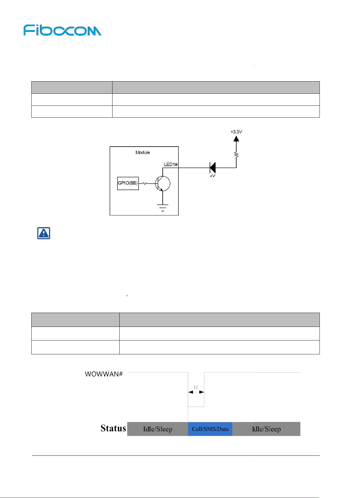
The LED#1 signal is used to indicate the operating status of the module, and the detailed description as
follows:
The resistance of LED current
The WOWWAN# signal is used to wake the Host (AP) when there comes the data request.The definition
of WOWWAN# signal is as follows:
The WOWWAN# timing is shown in Figure 3
LED1#
Low level (LED On)
High level (LED Off)
WOWWAN# Signal
Pull low 1s then pull high (pulse
High level
All Rights Reserved.
limiting resistor is selected according to the driving voltage and
3.7.1
LED#1Signal
shown in the following table:
Module Status
RF function ON
RF function OFF
The LED driving circuit is as
Signal
Figure 3-14 LEDDriving Circuit
Note:
-
the driving current.
3.7.2
Operating Mode
data requests
Idle/Sleep
WOWWAN#
-15:
signal).
L850-GL Hardware User Manual
Figure 3-15 WOWWAN#Timing
nc. written authorization -
Page 35 of 51
Page 36
Reproduction forbidden without Fibocom Wireless I
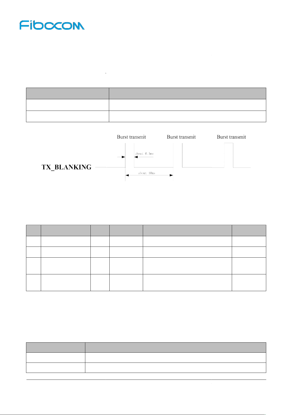
When the module operates in LTE TDD Band 39, TX_BLANKING outputs the pulse signal synchronous
As TDD TX may interfere the receiving of GPS signal, AP will disable GPS or stop GPS data receiving
when detecting TX_BLANKING pulse signal, so as to avoid abnormal operation of GPS.
s shown in Figure 3
Control
The L850 module provides four interrupt signals, and the pin definition is as follows:
The module provides a hardware pin to enable/disable WWAN RF function, and the function can also be
controlled by the AT command. The
definition of W_DISABLE1# signal is as follows:
Function
WWAN
WWAN function is disabled, the module entersFlight mode.
All Rights Reserved.
pulse signal synchronous with TDD burst TX
3.7.3
with TDD burst TX timing.
Operating Mode of Module
Default state
TDD burst TX(Band38)
TX_BLANKING
TX_BLANKING Signal
Low level
Output the
TX_BLANKING timing i
-16:
Figure 3-16 TX_BLANKING Timing
3.8
Interrupt
Pin Pin Name I/O
8
W_DISABLE1#
25 DPR
26 W_DISABLE2#
44 GNSS_IRQ
I
I
I
I
Reset Value Pin Description
PD
PU
PU
PD
Enable/Disable RF network
Body SAR detection
GNSS Disablesignal,
Reserved
GNSS Interrupt Request,
Reserved
3.8.1
W_DISABLE1#
Type
CMOS 3.3V
CMOS 1.8V
CMOS 1.8V
CMOS 1.8V
W_DISABLE1# signal
High/Floating
Low
L850-GL Hardware User Manual
nc. written authorization -
Page 36 of 51
Page 37
Reproduction forbidden without Fibocom Wireless I
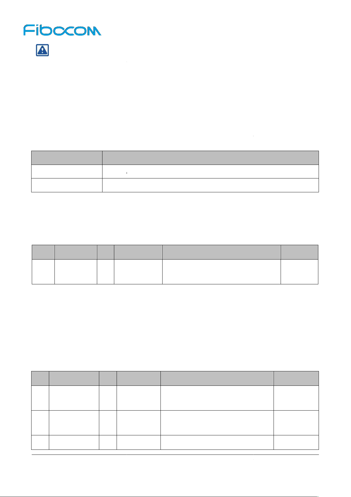
The function of W_DISABLE1# can be customized, please refer to the software porting guide.
The L850 module supportsBody SARfunction by detecting the DPR pin. The voltage level of DPR is high
sensor
As the result, the module then lowers down its emission power to its default threshold value, thus
reducing theRF radiation onthe human body. The threshol
Commands. The definition ofDPR signalas shown in the following
The L850 module supports a clock interface, itcan output 26MHz clock.
Reset Value
Interface
The module supports ANT Tunable interfaces with two different
GPO interface. Through cooperating with external antenna adapter switch via ANT Tunable, it can flexibly
configure the bands of LTE antenna to improve the antenna’s working efficiency and save space for the
Function
The module keeps the default emission power
Lower the maximum emission power to the threshold value of the module.
Reset Value
All Rights Reserved.
signal
26M clock output, default disabled
can be used for externalGPS, etc
Tunable ANT control,MIPI Interface,
Tunable ANT control,MIPI Interface,
Tunable ANT control,GPO interface,
Note:
3.8.2
by default, and when the SAR
DPR signal
High/Floating
Low
3.9
BODYSAR
ClockInterface
detects the closing human body, the DPR
table:
will be pulled down.
AT
Pin Pin Name I/O
46
SYSCLK
O
Pin Description
Type
1.8V
3.10
ANT Tunable
antenna.
Pin Pin Name I/O
RFE_RFFE2_
56
SCLK
RFE_RFFE2_
58
SDATA
59 ANTCTL0
O
O
O
Pin Description
RFFE2 clock,Open Drain output
RFFE2 data,Open Drain output
Type
CMOS
3.3/1.8V
CMOS
3.3/1.8V
CMOS 1.8V
L850-GL Hardware User Manual
nc. written authorization -
Page 37 of 51
Page 38
Reproduction forbidden without Fibocom Wireless I
Reset Value
Interface
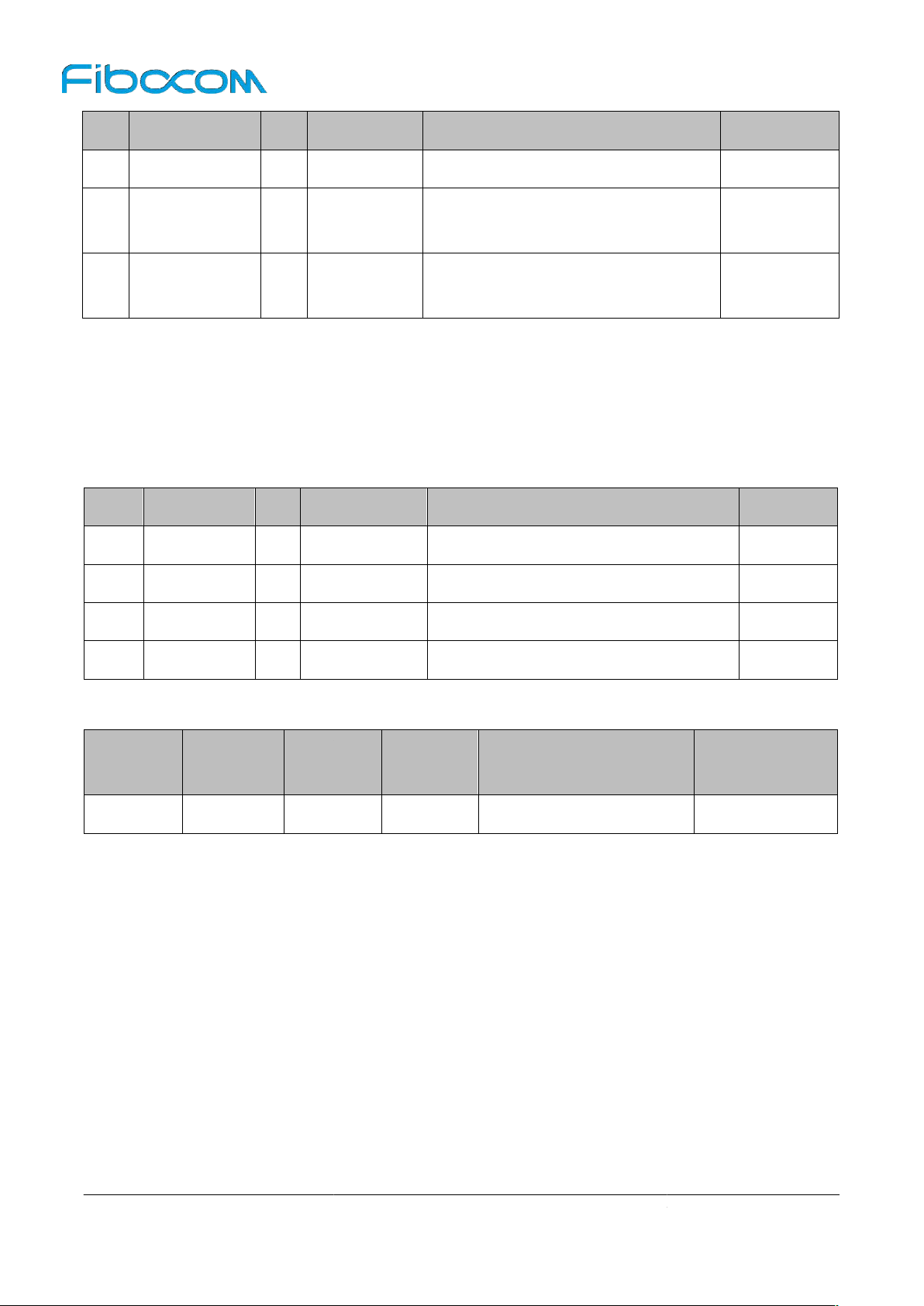
The L850 module provides four config pins for the
The M.2 module configuration as the following table:
Config_2
(pin75)
GND
Please refer to ”PCI Express M.2 Specification Rev1.0” for more details.
Interfaces
The module does not support other interfaces yet.
Reset Value
All Rights Reserved.
Tunable ANT control,GPO interface,
Tunable ANT control,GPO interface,
PCIe, USB3.0 type M.2
Module Type and Main
Pin Pin Name I/O
61 ANTCTL1
63 ANTCTL2
O
O
3.11
Config
module:
Pin Pin Name
1
CONFIG_3
21
CONFIG_0
69
CONFIG_1
75
CONFIG_2
I/O
O
L
O
L
O
L
O
Pin Description
Bit0
bit1
Bit2
configuration as the WWAN-
Pin Description
NC
Internally connected to GND
Internally connected to GND
Internally connected to GND
Type
CMOS 1.8V
CMOS 1.8V
Type
Config_0
(pin21)
GND GND
Config_1
(pin69)
Config_3
NC WWAN – PCIe,USB3.0
(pin1)
3.12
Other
Host Interface
Port
Configuration
0
L850-GL Hardware User Manual
nc. written authorization -
Page 38 of 51
Page 39
Reproduction forbidden without Fibocom Wireless I
Frequency
Functionality
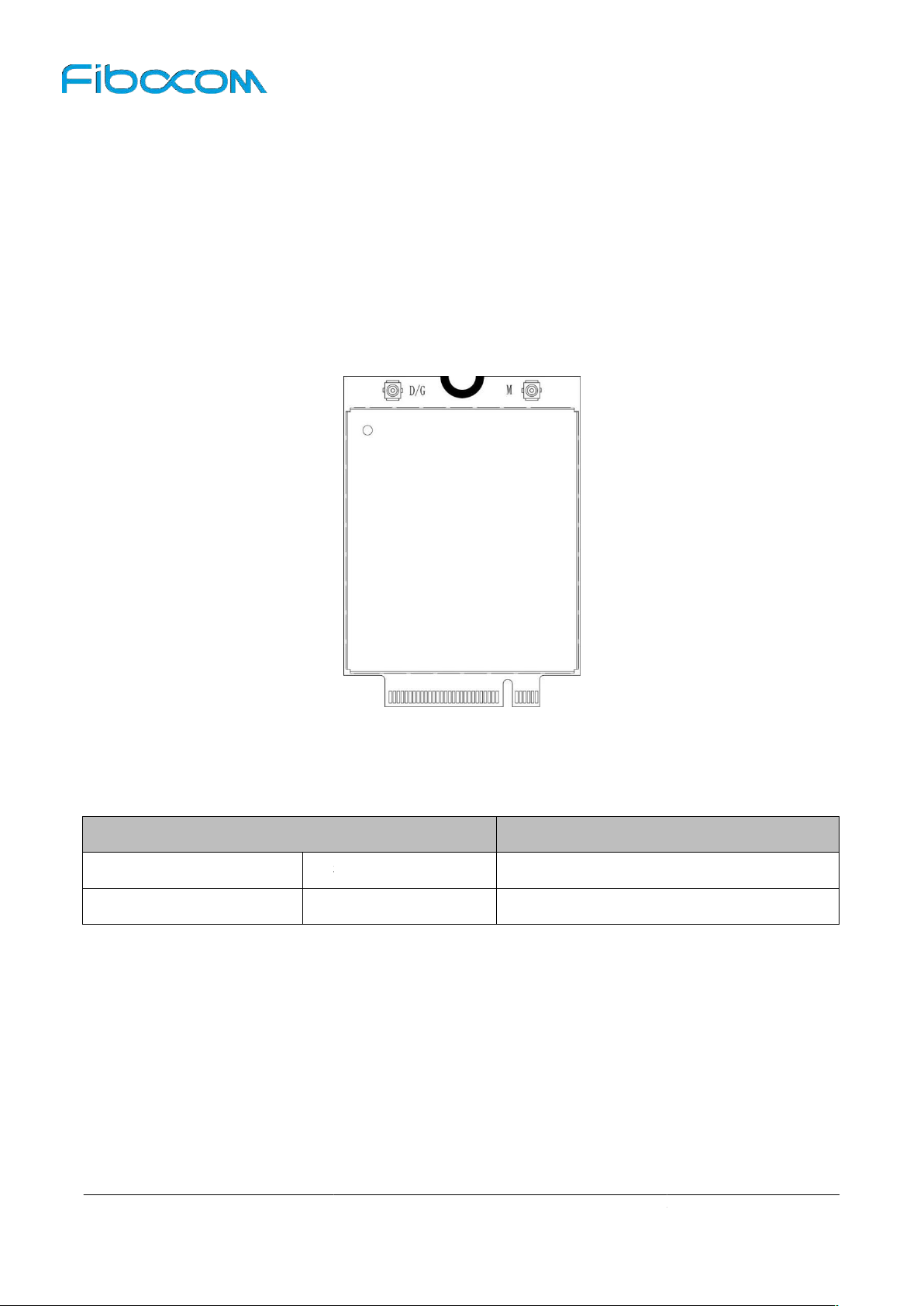
module supports two RF connectors used for external antenna connection. As the Figure 4
shows, “M” is for Main antenna, used to receive and transmit RF signals; “D/G” is for Diversity antenna,
used to receive the diversity RF signals.
Characteristic
DC to 6GHz
50Ω
Dimension
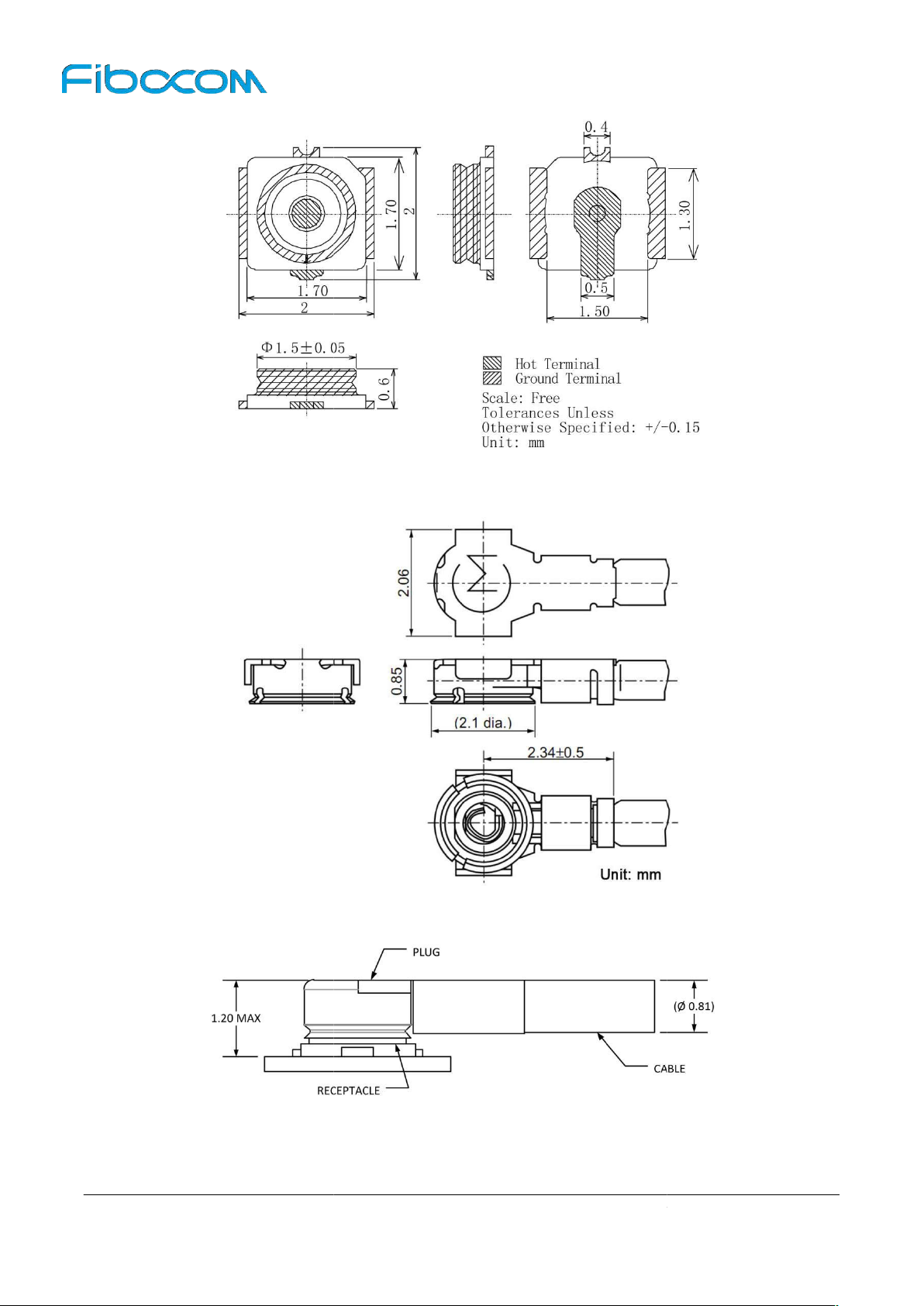
The L850 module adopts standard M.2 module RF connectors, the model name is
company, and the connector size is 2*2*0.6m. The connector dimension is shown as following picture:
All Rights Reserved.
Environment Condition
4 Radio
4.1
RF Interface
4.1.1
The L850
RF Interface
-1
Figure 4-1 RF connectors
4.1.2
Rated Condition
Frequency Range
Characteristic Impedance
4.1.3
RFConnector
RF Connector
Temperature Range
–40°C to +85°C
818004607
from ECT
L850-GL Hardware User Manual
nc. written authorization -
Page 39 of 51
Page 40
Reproduction forbidden without Fibocom Wireless Inc. written authorization
Figure 4
Figure 4
4 Schematic diagram of 0.81mm coaxial antenna connected to the RF connector
All Rights Reserved.
-2 RF connector dimensions
-3 0.81mm coaxial antenna dimensions
Figure 4-
L850-GL Hardware User Manual
-
Page 40 of 51
Page 41
Reproduction forbidden without Fibocom Wireless Inc. written authorization
Band
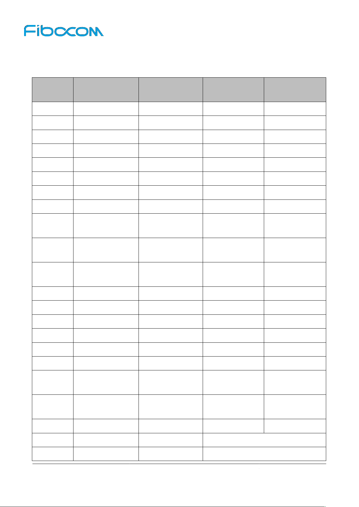
The L850 module operating bands of the antennas are as follows:
LSMH Blocks A/B/C
Japan Lower 800MHz
Japan Upper 800MHz
All Rights Reserved.
2570
1880
4.2
Operating
Operating
Band
Band 1 IMT 2100MHz
Band 2 PCS 1900MHz
Band 3 DCS 1800MHz
Band 4 AWS 1700MHz
Band 5 CLR 850MHz
Band 7 IMT-E 2600Mhz
Band 8 E-GSM 900MHz
Band 11 LPDC 1500MHz
Description
Band 12
700MHz
Band 13
USMH Block C
700MHz
Mode
LTE FDD/WCDMA 1920 - 1980
LTE FDD/WCDMA 1850 - 1910
LTE FDD 1710 - 1785
LTE FDD/WCDMA 1710 - 1755
LTE FDD/WCDMA 824 - 849
LTE FDD 2500 - 2570
LTE FDD/WCDMA 880 - 915
LTE FDD 1427.9 - 1447.9
LTE FDD
LTE FDD
Tx (MHz)
699 - 716
777 - 787
Rx (MHz)
2110 - 2170
1930 - 1990
1805 - 1880
2110 - 2155
869 - 894
2620 - 2690
925 - 960
1475.9 - 1495.9
729 - 746
746 - 756
Band 17
Band 18
Band 19
Band 20 EUDD 800MHz
Band 21 UPDC 1500MHz
Band 26 ECLR 850MHz
Band 28 APAC 700MHz
Band 29
Band 30
Band 66 1700MHz
Band 38 IMT-E 2600MHz
LSMH Blocks B/C
700MHz
LSMH blocks D/E
700MHz
WCS blocks A
2300MHz
LTE FDD
LTE FDD 815 - 830
LTE FDD 830 - 845
LTE FDD 832 - 862
LTE FDD 1447.9 - 1462.9
LTE FDD 814 - 849
LTE FDD 703 - 748
LTE FDD
LTE FDD
LTE FDD 1710 - 1780
LTE TDD
704 - 716
N/A
2305 - 2315
734 - 746
860 - 875
875 - 890
791 - 821
1495.9 - 1510.9
859 - 894
758 - 803
716 - 728
2350 - 2360
2110 - 2200
- 2620
Band 39 TDD 1900MHZ
L850-GL Hardware User Manual
LTE TDD
- 1920
-
Page 41 of 51
Page 42
Reproduction forbidden without Fibocom Wireless Inc. written authorization
BRS/EBS 2500MHZ
Power
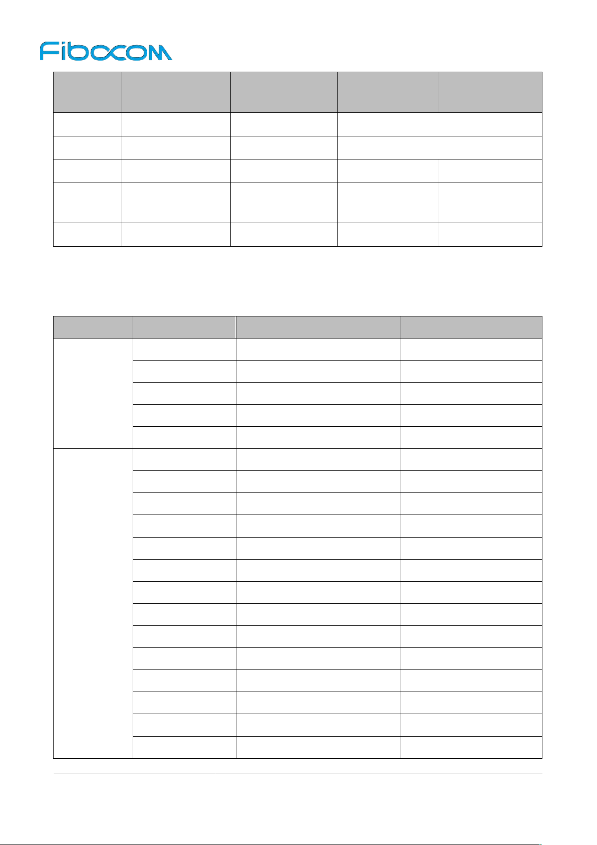
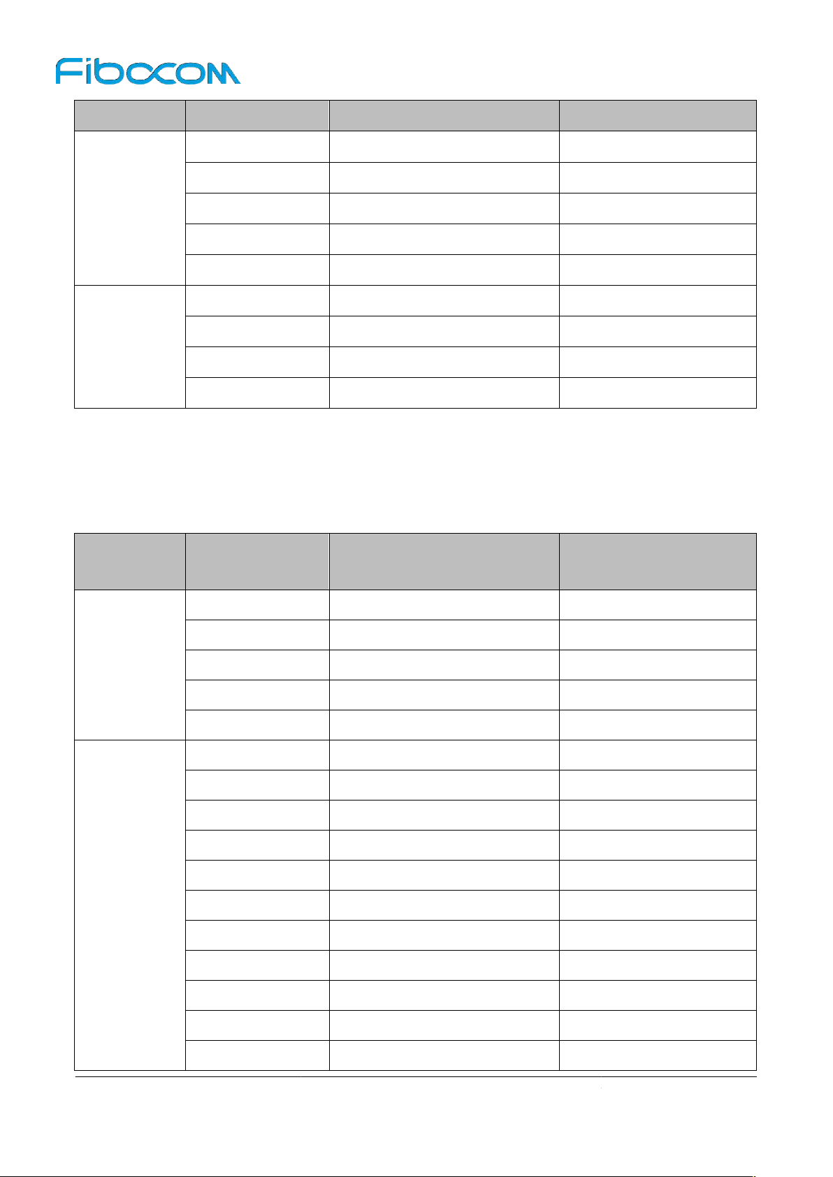
The transmitting power foreach band of the L850 moduleas shown in the following table:
All Rights Reserved.
2300
2496
10MHz Bandwidth, 1 RB
10MHz Bandwidth, 1 RB
10MHz Bandwidth, 1 RB
10MHz
10MHz Bandwidth, 1 RB
10MHz Bandwidth, 1 RB
10MHz Bandwidth, 1 RB
10MHz Bandwidth, 1 RB
10MHz Bandwidth, 1 RB
10MHz Bandwidth, 1 RB
10MHz
10MHz Bandwidth, 1 RB
10MHz Bandwidth, 1 RB
10MHz Bandwidth, 1 RB
Operating
Band
Description
Mode
Tx (MHz)
Rx (MHz)
Band 40 IMT 2300MHz
Band 41
GPS L1
GLONASS
L1
BeiDou
4.3
Transmitting
LTE TDD
LTE TDD
N/A
N/A
N/A
Mode Band
Band 1
WCDMA
Band 2
Band 4
Band 5
Tx Power(dBm) Note
23.5±1
23.5±1
23.5±1
23.5±1
- 2400
- 2690
1575.42±1.023
1602.5625±4
1561.098±2.046
LTE FDD
Band 8
Band 1
Band 2
Band 3
Band 4
Band 5
Band 7
Band 8
Band 11
Band 12
Band 13
Band 17
Band 18
23.5±1
23±1
23±1
23±1
23±1
23±1
23±1
23±1
23±1
23±1
23±1
23±1
23±1
Bandwidth, 1 RB
Bandwidth, 1 RB
Band 19
Band 20
L850-GL Hardware User Manual
23±1
23±1
-
Page 42 of 51
Page 43
Reproduction forbidden without Fibocom Wireless Inc. written authorization
Sensitivity
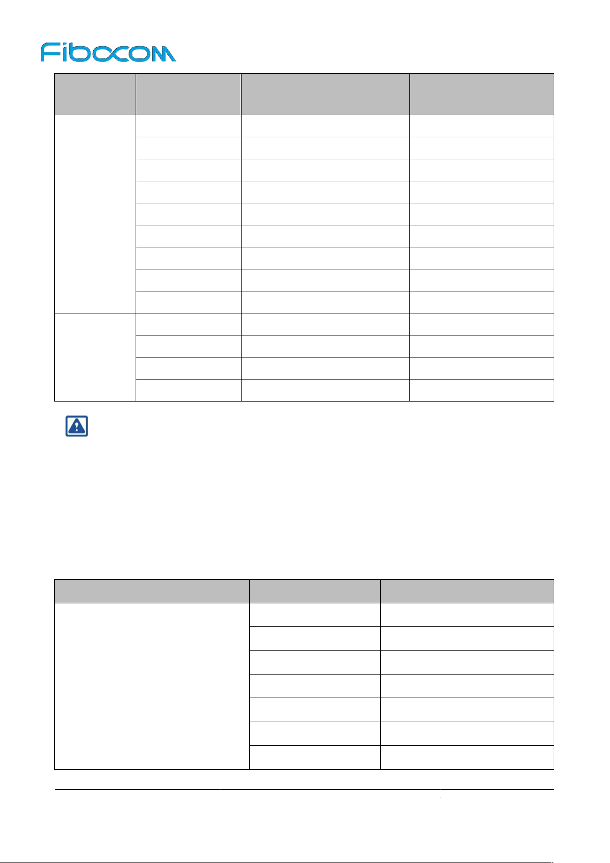
The receiver sensitivity foreach band of the L850 module as shown in the following table:
All Rights Reserved.
10MHz Bandwidth, 1 RB
10MHz Bandwidth, 1 RB
10MHz Bandwidth, 1 RB
10MHz Bandwidth, 1 RB
10MHz Bandwidth, 1 RB
10MHz Bandwidth, 1 RB
10MHz Bandwidth, 1 RB
10MHz Bandwidth, 1 RB
10MHz
BER<0.1%
BER<0.1%
BER<0.1%
BER<0.1%
BER<0.1%
10MHz Bandwidth
10MHz Bandwidth
10MHz Bandwidth
10MHz Bandwidth
10MHz Bandwidth
10MHz Bandwidth
10MHz
10MHz Bandwidth
10MHz Bandwidth
10MHz Bandwidth
10MHz Bandwidth
Mode Band
Tx Power(dBm) Note
Band 21
Band 26
Band 28
Band 30
Band 66
Band 38
23±1
23±1
23±1
23±1
23±1
23±1
LTE TDD
Band 39
Band 40
Band 41
23±1
23±1
23±1
4.4
Receiver
Bandwidth, 1 RB
Mode
WCDMA
LTE FDD
Band
Band 1
Band 2
Band 4
Band 5
Band 8
Band 1
Band 2
Band 3
Band 4
Band 5
Band 7
Band 8
Rx Sensitivity(dBm)
Typical
TBD
TBD
TBD
TBD
TBD
TBD
TBD
TBD
TBD
TBD
TBD
TBD
Note
Bandwidth
Band 11
Band 12
Band 13
Band 17
L850-GL Hardware User Manual
TBD
TBD
TBD
TBD
-
Page 43 of 51
Page 44
Reproduction forbidden without Fibocom Wireless Inc. written authorization
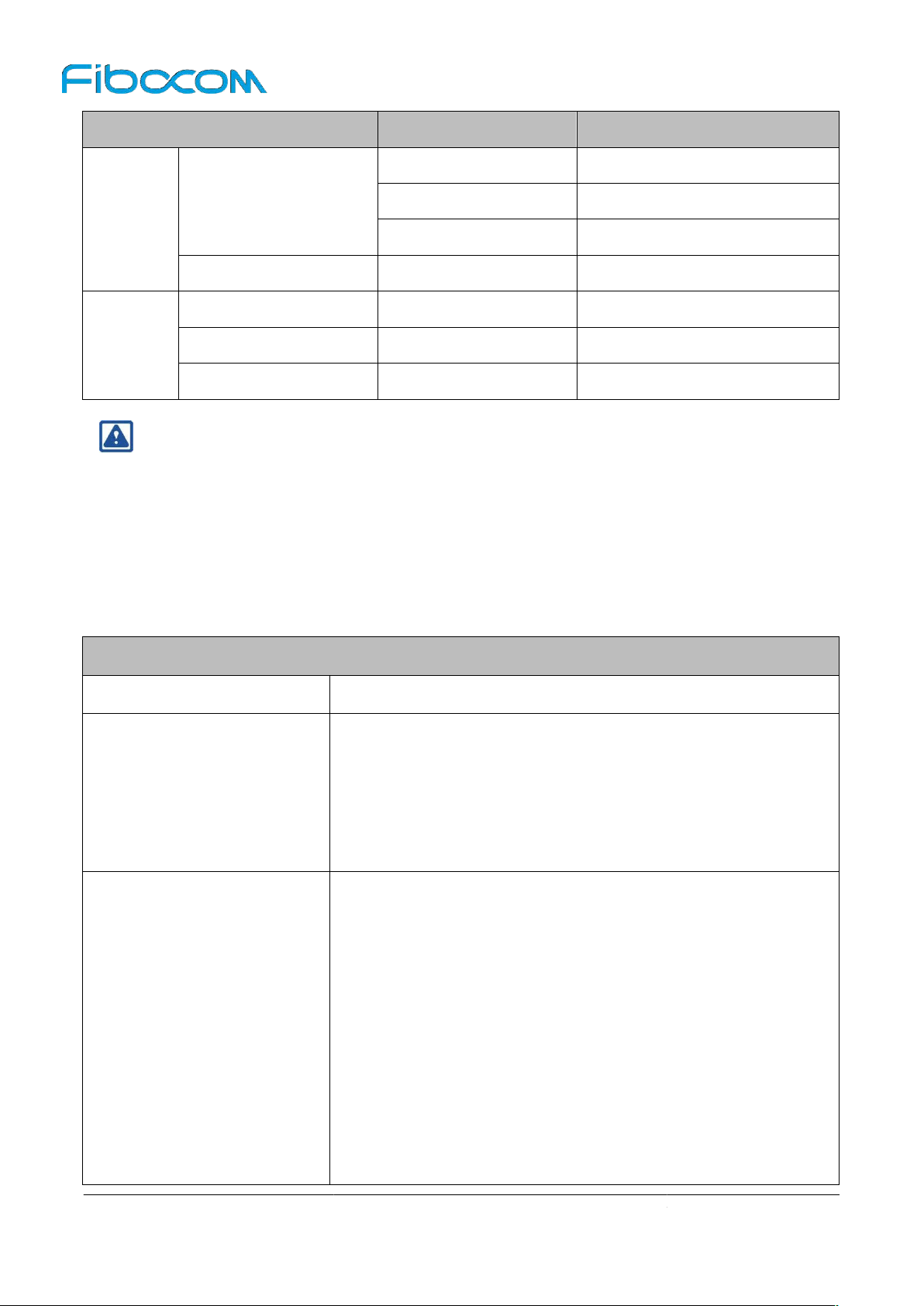
The above values are measuredfor the dual antennas situation(Main+Diversity). For single main
antenna (without Diversity), the sensitivity will drop around
L850 module supports GNSS/BeiDou and
All Rights Reserved.
10MHz Bandwidth
10MHz Bandwidth
10MHz Bandwidth
10MHz Bandwidth
10MHz Bandwidth
10MHz Bandwidth
10MHz Bandwidth
10MHz Bandwidth
10MHz Bandwidth
10MHz Bandwidth
10MHz Bandwidth
10MHz Bandwidth
10MHz Bandwidth
Test Result
Mode
Band
Band 18
Rx Sensitivity(dBm)
Typical
TBD
Note
LTE TDD
Band 19
Band 20
Band 21
Band 26
Band 28
Band 29
Band 30
Band 66
Band 38
Band 39
Band 40
Band 41
Note:
TBD
TBD
TBD
TBD
TBD
TBD
TBD
TBD
TBD
TBD
TBD
TBD
4.5
GNSS
integrated antenna.
Description
Power
Condition
GPS fixing TBD
GPS tracking TBD
GLONASS fixing TBD
GLONASS tracking TBD
BeiDou fixing TBD
BeiDou tracking TBD
Sleep TBD
L850-GL Hardware User Manual
-
Page 44 of 51
Page 45
Reproduction forbidden without Fibocom Wireless Inc. written authorization
GPS/GLONASS/BeiDou
Please note that GPS current is tested with RF disabled.
Design
The L850module provides main and diversity antenna
L850 module Main antenna requirements
All Rights Reserved.
Test Result
The most proper antenna to adapt the frequencies should
Description
TTFF
AGNSS
GPS
Condition
Cold start TBD
Warm start TBD
Hot Start TBD
Cold start TBD
Open Sky TBD
Sensitivity
4.6
Antenna
GLONASS
BeiDou
Note:
Open Sky TBD
Open Sky TBD
as shown in the following table:
Frequency range
Bandwidth(WCDMA)
Bandwidth(LTE)
WCDMA band 1(2100) : 250 MHz
WCDMA band 2(1900) : 140 MHz
WCDMA band 4(1700) : 445 MHz
WCDMA band 5(850) : 70 MHz
WCDMA band 8(900) : 80 MHz
LTE band 1(2100): 250 MHz
LTE band 2(1900): 140MHz
LTE Band 3(1800): 170 MHz
LTE band 4(1700): 445MHz
LTE band 5(850): 70 MHz
LTE band 7(2600): 190 MHz
be used.
LTE Band 8(900): 80 MHz
LTE Band 11(1500): 68 MHz
LTE Band 12(700): 47 MHz
LTE Band 13(700): 41 MHz
L850-GL Hardware User Manual
-
Page 45 of 51
Page 46
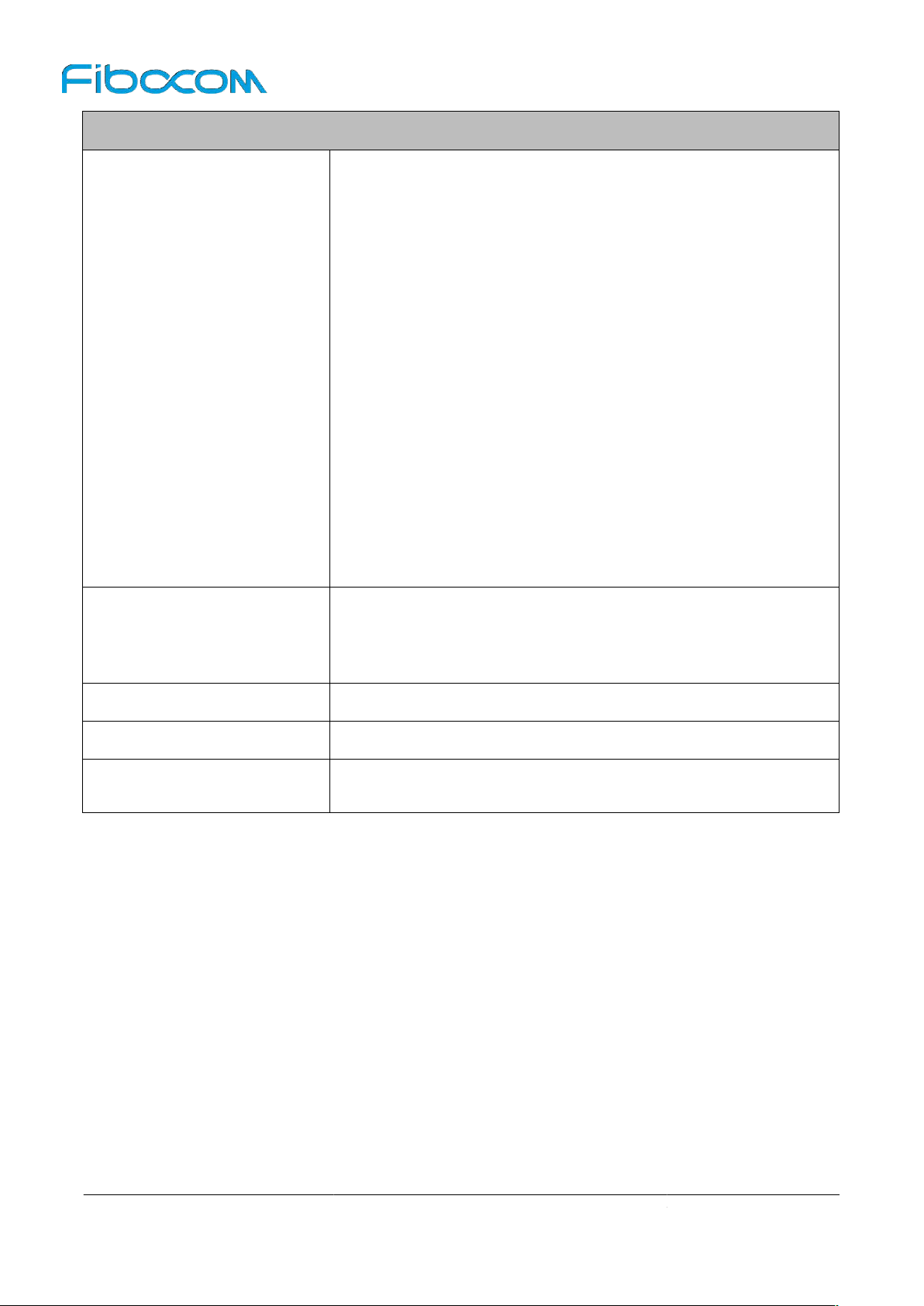
Reproduction forbidden without Fibocom Wireless Inc. written authorization
L850 module Main antenna requirements
All Rights Reserved.
Bandwidth(GNSS/BeiDou)
LTE Band 17(700): 42 MHz
LTE Band 18(800): 80 MHz
LTE Band 19(800): 80 MHz
LTE band 20(800): 71 MHz
LTE band 21(1500): 63 MHz
LTE band 26(850): 80 MHz
LTE band 28(700): 100 MHz
LTE band 29(700): 12 MHz
LTE band 30(2300): 55 MHz
LTE band 66(1700): 490MHz
LTE band 38(2600): 50 MHz
LTE Band 39(1900): 40 MHz
LTE band 40(2300): 100 MHz
LTE band 41(2500): 194 MHz
GPS: 2MHz
GLONASS: 8MHz
Impedance
Input power
Recommended standing-wave
ratio (SWR)
BeiDou: 4MHz
50Ohm
> 26dBmaverage power WCDMA & LTE
≤ 2:1
L850-GL Hardware User Manual
-
Page 46 of 51
Page 47
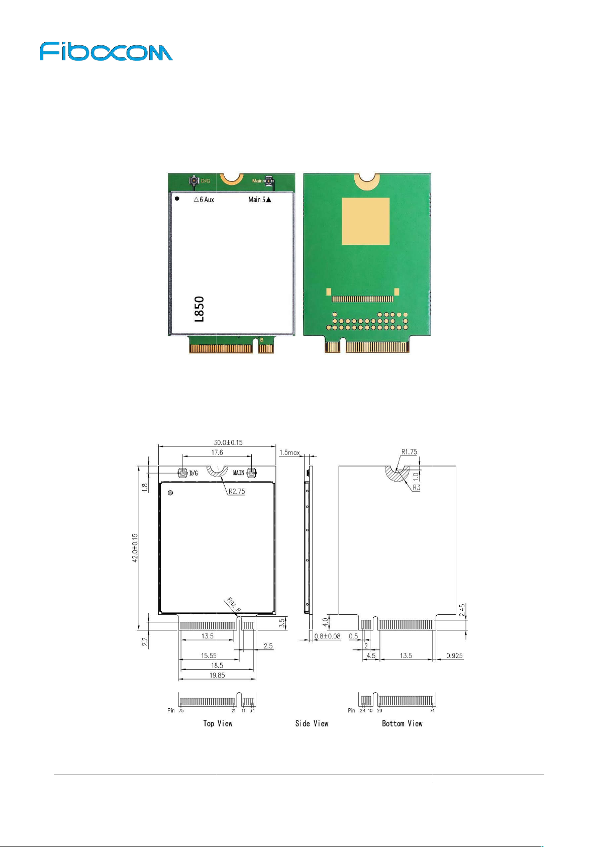
Reproduction forbidden without Fibocom Wireless Inc. written authorization
Specification
Appearance
The product appearance for L850 module is shown in Figure5
Structure
The structuraldimensionof the L850 module is shown in Figure 5
All Rights Reserved.
5 Structure
5.1
Product
Figure 5-1 Module Appearance
-1:
5.2
Dimension of
-2:
Figure 5-2 Dimension of Structure
L850-GL Hardware User Manual
-
Page 47 of 51
Page 48
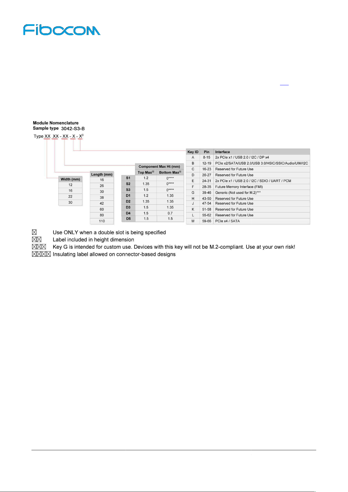
Reproduction forbidden without Fibocom Wireless Inc. written authorization
Model
pin gold finger as external interface, where 67 pins are signal pins and 8
pins are notch pins as shown in Figure 3
on, L850 module adopts Type 3042
maximum height on t top layer is 1.5mm, PCB thickness is 0.8mm, and KEY ID is B).
The L850 module connects to AP via M.2 connector, it is recommended to use M.2 conn
LOTES company with the model APCI0026
All Rights Reserved.
1. For module dimension, please refer to chapter
B interface (30x42mm, the component
3. The package of connector,
5.3
M.2 Interface
The L850 M.2 module adopts 75-
the M.2 interface definiti
-
-S3-
5.2. Based on
5.4
M.2 Connector
please refer to the specification.
-P001A as shown in Figure 5-
ector from
L850-GL Hardware User Manual
-
Page 48 of 51
Page 49
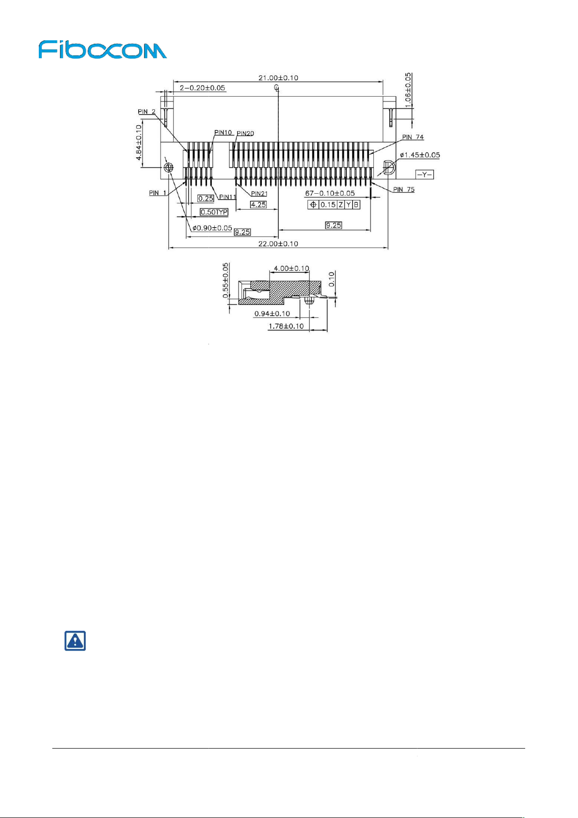
Reproduction forbidden without Fibocom Wireless Inc. written authorization
Figure 5
Storage Conditions (recommended): Temperature is 23 ± 5
Storage period (sealed vacuum packing): Under the recommended storage conditions, the storage life is
The L850 module uses the tray sealed vacu
the hard cartoon box, so that the storage, transportation and the usage of modules can be protected to
The module is a precision electronic product, and may suffer
electrostatic protection measures are taken.
All Rights Reserved.
, relative humidity is RH 35
-3 M.2 Dimension of Structure
5.5
Storage
5.5.1 Storage Life
12 months.
℃
-70%.
5.6
Packing
the greatest extent.
Note:
L850-GL Hardware User Manual
-
Page 49 of 51
Page 50
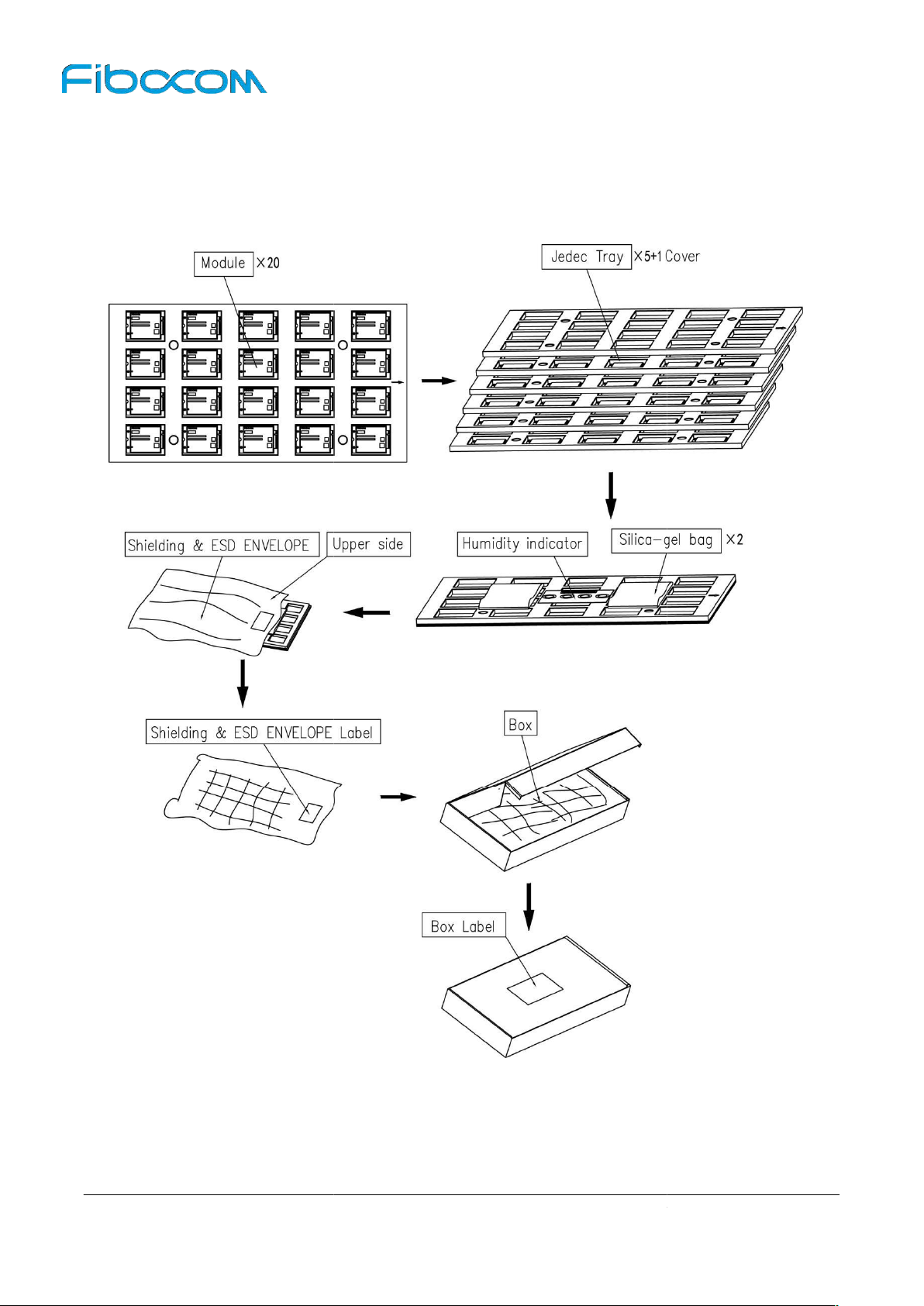
Reproduction forbidden without Fibocom Wireless Inc. written authorization
The L850 module uses tray package,20 pcs are packed in each tray, with 5 trays in each box and 6 boxes
in each case. Tray packaging process is shown
All Rights Reserved.
5.6.1
Tray Package
in Figure 5-4:
Figure 5-4 Tray Packaging Process
L850-GL Hardware User Manual
-
Page 50 of 51
Page 51
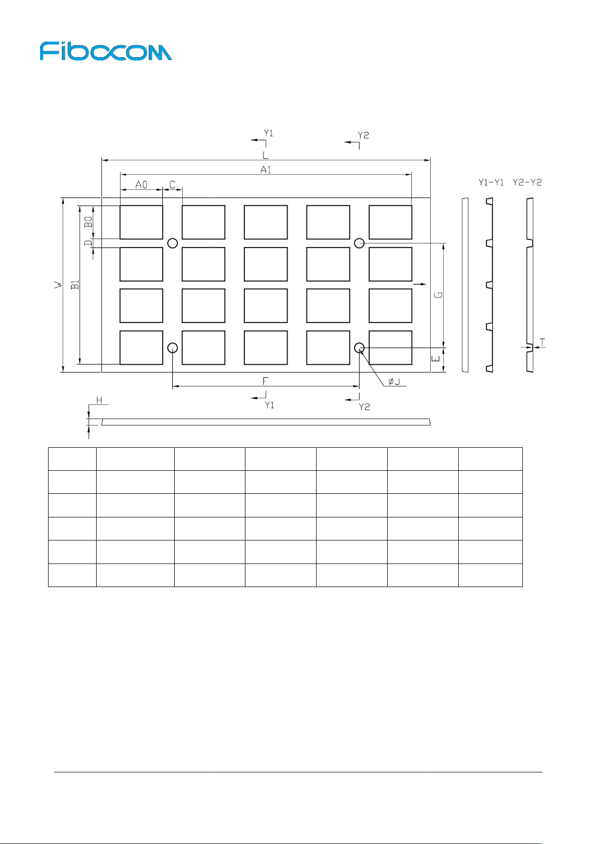
Reproduction forbidden without Fibocom Wireless Inc. written authorization
pallet size is 330*175*6.0mm, as shown in Figure 5
175.0±0.5
B1
159.0±0.3
9.0±0.2
All Rights Reserved.
43±0.3
24.5±0.5
5.6.2
The
Tray size
-5:
ITEM
DIM 330.0±0.5
ITEM A1
DIM 294.0±0.3
ITEM
DIM 105.0±0.2
G
L
W
H
6.0±0.3 0.5±0.1
C
20.0±0.5 9.0±0.5
J
T
A0
D
33.0±0.3
E
187.5±0.2
B0
F
Figure 5-5Tray Size (Unit: mm)
L850-GL Hardware User Manual
-
Page 51 of 51
 Loading...