


H330 HSPA+ Module
Hardware User Manual
Version: V1.0.0
Date: 2012-05-29
n
m
g
t
,
n
a
©
n
V
1
a
m
©
t
s
f
t
c
o
c
e
s
y
s
a
n
o
o
n
o
G
9
b
o
G
n
a
g
o
o
h
r
n
e
r
S
o
o
p
t
b
m
s
m
G
e
n
p
o
e
a
t
a
o
t
a
o
p
s
h
p
t
s
t
s
m
o
b
t
O
u
e
d
l
Confide
This docu
(Fibocom).
engineerin
requiremen
subject to c
of G&T.
Copyrig
Transmittal
contents a
be held liab
or design p
Copyright
tial Ma
ent contain
Fibocom of
efforts that
s specifical
hange. Dis
ht
reproducti
d communi
le for paym
tent are re
1999-2010
erial
informatio
ers this inf
use the pr
ly provided
losure of th
n, dissemi
ation there
nt of dama
erved.
Shenzhen
highly co
rmation as
ducts desi
to Fibocom
is informati
ation and/
f to others
ges. All rig
&T Indust
fidential to
service to
ned by Fib
by the cust
n to other
r editing of
without exp
ts created
ial Develop
henzhen
its custom
com. The i
mers. All s
arties is pr
his docum
ress authori
y patent gr
ent Co., L
&T Industri
rs, to supp
formation
ecification
hibited wit
nt as well a
zation are
nt or regist
d. All right
l Develop
rt applicati
rovided is
supplied h
out the writ
s utilization
rohibited.
ration of a
reserved.
ent Co., Lt
n and
ased upon
erein are
en consent
of its
ffenders wi
tility model
l
Revisio
Tradem
The FIBOC
service na
Copyright
Histor
e
rsion
V
.0.0
rks Not
OM Logo is
es or Logo
1999-2012
Date
2012-05-2
ice
registered
are the pr
Shenzhen
Initial
y Shenzhe
perty of th
&T Indust
G&T Indu
ir respectiv
ial Develop
Rem
trial Devel
e owners.
ent Co., L
rks
pment Co.,
d. All right
Ltd. All oth
reserved.
r product o
r
H330 HSPA+
Module Hard
ware User M
nual
Page 2 of 44

e
S
S
P
P
P
n
D
R
a
B
P4.24.2
a
P5.15.1
1
1
O
2
25.25.2
3
3
U5.4
4
s
e
p
d
a
o
M
D
e
f
T
e
C
e
D
e
e
e
g
D
a
c
a
g
p
p
c
p
C
.
.
.
.
.
.
.
.
.
g
.
.
.
.
.
.
.
.
.
.
.
.
.
.
.
.
.
.
.
.
.
.
.
s
.
.
.
.
.
.
.
.
.
.
.
.
.
.
.
.
.
.
.
.
.
.
.
.
.
.
.
.
.
.
.
.
5
5
5
6
6
6
0
1
1
2
3
3
4
4
4
0
0
0
1
4
4
5
5
6
6
7
8
8
9
0
0
0
1 Prefac
1.1
1.2
2 Introdu
2.1
2.2
2.3
3 Macha
3.1
3.2
4 Hardw
4.1
4.2
.................
cope ........
tandards ..
ction ..........
roduct De
roduct Sp
roduct Ap
ical ...........
imension .
ecommen
re Scope ..
lock Diagr
in Definiti
.1 Pin
..................
..................
..................
..................
cription .....
cification ...
earance ....
..................
..................
PCB Desi
..................
m .............
n ...............
ap ............
..................
..................
..................
..................
..................
..................
..................
..................
..................
n ..............
..................
..................
..................
..................
ontent
..................
..................
..................
..................
..................
..................
..................
..................
..................
..................
..................
..................
..................
..................
..................
..................
..................
..................
..................
..................
..................
..................
..................
..................
..................
..................
..................
..................
..................
..................
..................
..................
..................
..................
..................
..................
..................
..................
..................
..................
..................
..................
..................
..................
..................
..................
..................
..................
..................
..................
..................
..................
..................
..................
..................
..................
................
................
................
................
................
................
.............. 1
............... 1
............... 1
.............. 1
.............. 1
.............. 1
.............. 1
.............. 1
5 Hardw
5.1
5.
5.
5.2
5.
5.
5.3
5.
5.
.2 Pin
re Interfac
ower Inter
.1 VBA
.2 Pow
.3 VIO .
.4 VRT
n/Off/Res
.1 Pin
.2 Pow
.3 Pow
.4 Res
Indicator Si
.1 Pin
.2 Indic
escription ..
.................
ace ...........
.................
r Consum
..................
................
t................
escription ..
r on ..........
r off ...........
t ................
nal ............
escription ..
tor Descri
..................
..................
..................
..................
tion ...........
..................
..................
..................
..................
..................
..................
..................
..................
..................
tion ...........
..................
..................
..................
..................
..................
..................
..................
..................
..................
..................
..................
..................
..................
..................
..................
..................
..................
..................
..................
..................
..................
..................
..................
..................
..................
..................
..................
..................
..................
..................
..................
..................
..................
..................
..................
..................
..................
..................
..................
..................
..................
..................
..................
..................
..................
..................
..................
..................
..................
..................
..................
..................
..................
..................
..................
..................
..................
..................
..................
..................
.............. 1
.............. 2
.............. 2
.............. 2
.............. 2
.............. 2
.............. 2
.............. 2
.............. 2
.............. 2
.............. 2
.............. 2
.............. 2
.............. 2
.............. 2
5.4
H330 HSPA+
SB Interfa
.1 USB
5.
.2 USB
Module Hard
e ..............
Pin Descri
Design ......
ware User M
..................
tion ...........
..................
nual
..................
..................
..................
..................
..................
..................
..................
..................
..................
..................
..................
..................
.............. 3
.............. 3
.............. 3
Page 3 of 44

U5.55.5
U5.65.6
6
6
A
7
7
D5.85.8
O
c
E
E
e
O7.1
1
R7.2
2
A7.37.3
T
T
M
M
M
M
i
D
o
o
h
n
r
e
r
a
o
c
e
e
e
a
.
.
.
.
.
.
.
.
.
.
.
.
.
.
.
.
.
.
.
.
.
.
.
.
.
.
.
.
.
.
.
.
.
.
.
.
.
.
.
.
.
.
.
.
.
.
.
.
.
.
.
.
.
.
.
1
1
2
3
3
3
4
5
5
5
6
7
8
8
8
9
9
9
0
0
0
0
1
1
1
1
1
3
5.5
5.6
5.7
5.8
5.9
ART .........
.1 UAR
.2 UAR
SIM .........
.1 USI
.2 USI
5.
.3 USI
5.
.4 USI
nalog Aud
5.
.1 Pin
5.
.2 Audi
igital Audi
.1 I2S ..
.2 I2C ..
ther .........
..................
Interface .
Design ....
..................
Interface ..
Design .....
Design N
Hot Plug ..
o ...............
escription ..
Descriptio
................
..................
..................
..................
..................
..................
..................
..................
..................
..................
tice ...........
..................
..................
..................
n ................
..................
..................
..................
..................
..................
..................
..................
..................
..................
..................
..................
..................
..................
..................
..................
..................
..................
..................
..................
..................
..................
..................
..................
..................
..................
..................
..................
..................
..................
..................
..................
..................
..................
..................
..................
..................
..................
..................
..................
..................
..................
..................
..................
..................
..................
..................
..................
..................
..................
..................
..................
..................
..................
..................
..................
..................
..................
..................
..................
..................
..................
..................
..................
..................
.............. 3
.............. 3
.............. 3
.............. 3
.............. 3
.............. 3
.............. 3
.............. 3
.............. 3
.............. 3
.............. 3
.............. 3
.............. 3
.............. 3
.............. 3
6 Electri
6.1
6.2
7 RF Int
7.1
7.
7.2
7.
7.3
al and Envi
lectrical C
nvironme
rface .........
perational
.1 Main
.2 Dive
F PCB De
.1 Layo
.2 Impe
ntenna D
.1 Main
.2 Dive
ronmental ..
aracteristi
tal Charact
..................
Band ........
Antenna ....
sity ............
sign ...........
ut Guidelin
dance ........
sign ...........
Antenna D
sity antenn
..................
.................
ristic .........
..................
..................
..................
..................
..................
.................
..................
..................
sign Requi
design ....
..................
..................
..................
..................
..................
..................
..................
..................
..................
..................
..................
rement .......
..................
..................
..................
..................
..................
..................
..................
..................
..................
..................
..................
..................
..................
..................
..................
..................
..................
..................
..................
..................
..................
..................
..................
..................
..................
..................
..................
..................
..................
..................
..................
..................
..................
..................
..................
..................
..................
..................
..................
..................
.............. 3
.............. 3
.............. 3
.............. 4
.............. 4
.............. 4
.............. 4
.............. 4
.............. 4
.............. 4
.............. 4
.............. 4
.............. 4
H330 HSPA+
Module Hard
ware User M
nual
Page 4 of 44

a
o
a
a
o
r
n
T
T
D
T
T
n
T
T
c
T
2
T
T
T
T
T
T
e
T
c
T
T
T
h
u
r
f
c
0
n
E
a
o
H
c
c
r
U
e
g
D
p
S
M
(
e
n
b
a
d
+
s
e
S
n
p
n
m
o
d
c
S
a
a
o
i
S
e
o
n
S
h
r
a
r
c
v
m
n
y
a
B
S
n
p
o
n
o
s
a
e
o
S
S
M
m
O
p
e
n
D
y
w
q
S
o
p
h
r
o
e
n
s
1 Pref
1.1 Sc
This manu
the H330 H
This manu
availability
and softwa
1.2 Sta
3GPP
3GPP
(DTE-
3GPP
3GPP
radio i
SPA+ mod
ce
pe
l provides t
l gives a co
f any featu
e version o
dards
S 27.007
S 27.005
CE) interfa
S 23.040
S 24.011
terface
e electrical
le in a host
mplete set
e or functio
a specific
-v6.9.0: AT
-v6.0.1: Us
e for Short
-v6.9.0: Te
-v6.1.0: Po
, mechanic
application.
f hardware
n, which is
330 HAPA
command
e of Data T
Message
hnical reali
int- to - Poi
l and envir
features a
escribed in
module.
et for User
rminal Equ
ervice (SM
zation of S
t (PP) Sho
nmental re
d functions
this manua
Equipment
pment -Dat
) and Cell
ort Messag
t Message
quirements
that may b
l, depends
(UE)
a Circuit ter
roadcast
e Service (
ervice (S
for properl
provided b
n the hard
minating E
ervice (CB
MS)
S) support
integrating
y H330. Th
are revisio
uipment
)
n mobile
3GPP
3GPP
3GPP
resele
3GPP
Stage
3GPP
3GPP
3GPP
3GPP
3GPP
3GPP
Modul
3GPP
specifi
TS 25.3
S 27.010
S 27.060
tion in con
S 25.308
S 25.309
S 23.038
S 21.111
S 31.111
S 45.002
S 51.014
- Mobile
S 51.010
ation
-v6.0.0: Te
-v6.0.0: Pa
4-v6.10.0:
ected mod
-v6.4.0: Hi
-v6.6.0: F
-v6.1.0: Al
-v6.3.0: US
-v6.11.0 "U
-v6.12.0:
-v4.5.0: Sp
quipment
-1 -v6.7.0:
minal Equi
cket domai
ser Equip
h Speed D
D enhance
habets and
IM and IC
IM Applic
ultiplexing
ecification
SIM-ME) in
Mobile Stat
ment to Us
; Mobile St
ent (UE) p
wnlink Pa
uplink; O
language -
ard require
tion Toolkit
nd multip
f the SIM A
terface
on (MS) co
er Equipme
tion (MS) s
ocedures i
ket Access
erall descri
specific inf
ents
(USAT)"
le access o
pplication T
formance
nt (TE-UE)
upporting P
idle mode
(HSDPA);
tion; Stage
rmation
the radio
olkit for th
pecificatio
ultiplexer
acket Switc
and proced
verall desc
2
ath
Subscribe
; Part 1: C
rotocol
ed service
ures for cell
ription;
Identity
nformance
3GPP
3GPP
3GPP
H330 HSPA+
S 22.004
S 23.090
S 24.008
Module Hard
-v6.0.0: G
-v6.1.0: U
v6.19, Mo
ware User M
neral on su
structured
ile radio int
nual
pplementar
upplement
rface Laye
services
ry Service
r 3 specific
Data (USS
tion;
); Stage 2
Page 5 of 44
o
d
S
0
d
F
e
:
m
n
s
z
e
U
0
G
0
5
2
G
E
m
3
g
a
n
A
D
z
o
A
0
0
5
C
2
a
u
s
.
t
A
m
C
/
e
s
A
z
1
S
a
S
A
2 Intr
2.1 Pro
H330 is a h
GSM/GPR
850/900/19
2.2 Pro
Product
Support
ductio
uct De
igh integrity
/EDGE GS
0/2100MH
uct Sp
eatures
d Bands:
• 4 Band
850/90
• 4 Band
850/90
criptio
3G WCDM
M850/900/
.
cificati
MTS/HSP
/1900/210
SM
/1800/190
wireless
CS1800/P
n
(WCDMA
MHz
MHz
odule, LG
S1900MH
FDD)
package,
and UMT
20 pin. It c
/HSDPA/H
n support
UPA/HSP
+
Data:
Physical
• UMTS/H
• HSUPA
• HSDPA
• GSM 3
• EDGE (
• GPRS
• Size:3
• Height:
• Mountin
• Weight:
SDPA/HSU
.76Mbps (
1Mbps (C
PP release
-GPRS) m
ulti-slot cla
.8mm x 27
2.45 mm
:LGA
< 6 grams
PA 3GPP r
at 6)
t 14)
7
lti-slot clas
s 12
8mm
lease 7
12
Environ
H330 HSPA+
ental
• Operatin
Module Hard
g Tempera
ware User M
ure:-30℃
nual
~ +65℃
Page 6 of 44

a
g
C
r
t
o
v
o
e
0
0
5
8
c
1
u
t
y
v
a
r
S
3
C
H
z
d
d
3
2
2
m
P
Perform
Operatin
Current
Tx Powe
• Storage
nce
Voltage
• Voltage:
onsumpti
• 2mA (Sl
• 3G Idle:
• 3G Talk:
• 2G Talk:
(Typical)
• UMTS/H
• GSM 85
Temperatu
3.6 ~ 4.2V
n(Typical)
ep Mode)
35mA
500mA
260mA (G
SPA Class
/900 MHz
e:-40 ~℃
M PCL5)
(24dBm)
lass4 (33
+85℃
Bm)
Rx Sensi
Interface
Connect
Connecti
• GSM 18
• EDGE 8
• EDGE 1
ivity(Typi
• UMTS/H
• GSM:-
rs
• RF Thro
• Main An
• Diversit
ity
0/1900 M
0/900 MH
00/1900 M
al)
SPA:-109
07dBm
gh Pads in
enna
Antenna
z Class1 (
Class E2 (
Hz Class E
Bm
LGA, 2 x
0dBm)
7dBm)
(26dBm)
ini-UFL in
CIe model
• 1*USB 2
.0
• 2*UART
H330 HSPA+
Module Hard
ware User M
nual
Page 7 of 44
t
V
a
p
p
p
e
n
w
t
4
S
t
4
S
T
a
n
a
a
p
t
a
C
t
a
1
P
a
Data Fea
HSPA+
EDGE
• MUX Ov
• Multiple
• SPI Sup
• I2C Sup
• I2S Sup
ures
• Embedd
• Max upli
• Max do
• Multi-slo
er UART1
Profiles ove
ort
ort
ort
d TCP/IP
k 5.76Mbp
nlink 21Mb
class 12
r USB
nd UDP/IP
s
s
protocol st
ck
GPRS
CSD
SMS
(4 Down;
• Coding
• Multi-slo
(4 Down;
• Coding
• UMTS
• GSM
• MO / M
• Cell bro
Up; 5 Tot
cheme M
class 12
Up; 5 Tot
cheme CS
Text and
dcast
l)
S1-MCS9
l)
-CS4
DU modes
oice Fe
H330 HSPA+
tures
• Telepho
Module Hard
y
ware User M
nual
Page 8 of 44
o
S
m
r
a
o
a
p
u
e
c
.
.
e
e
p
a
A
H
o
B
Audio C
Characte
• Analog
• Voice c
ntrol
• Broad g
• Echo su
• Noise s
• Side ton
r Set
• IRA
• GSM
• UCS2
• HEX
nd Digital
ders EFR/
in control
pression
ppression
udio
R/FR/AMR
Control/
AT Com
Accesso
tatus Indi
• GPIO’s
• A/D
• RTC
and Set
• G&T pro
• GSM 07
• GSM 07
ies
• Firmwar
• User Ma
• Develop
ations
prietary AT
05
07
Loader T
nual
r Kit
commands
ol over US
/UART
Regulato
ry and Ap
rovals
• FCC
H330 HSPA+
Module Hard
ware User M
nual
Page 9 of 44
d
H
e
m
w
• RoHS
p
u
w
a
e
a
w
4
• CE
• RRB
2.3 Pro
H330
Top Vi
Botto
uct Ap
SPA+ Mod
w:
View:
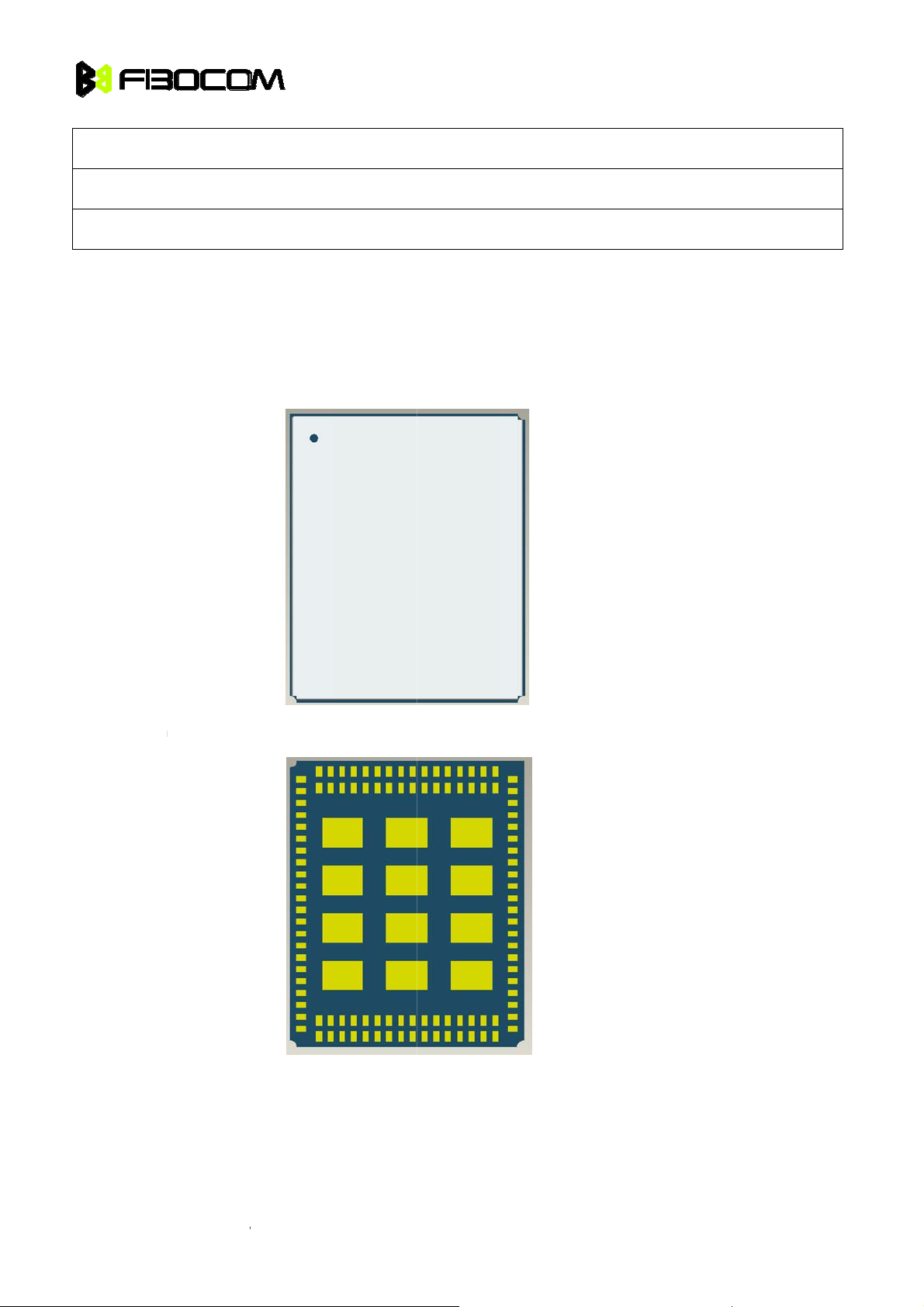
earanc
le Appear
nce is belo
。
H330 HSPA+
Module Hard
are User M
nual
Page 10 of 4
h
m
w
w
w
4
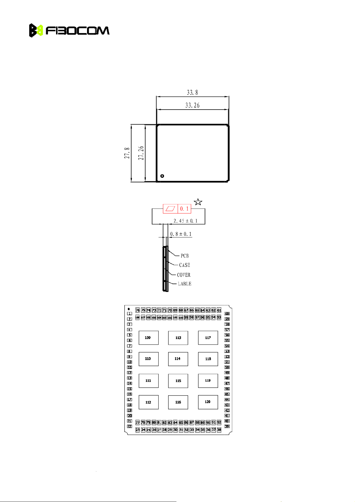
3 Mec
3.1 Di
anical
ension
Top View
Side View
Bottom Vie
H330 HSPA+
Module Hard
are User Manual
Page 11 of 4
c
w
d
w
a
e
4
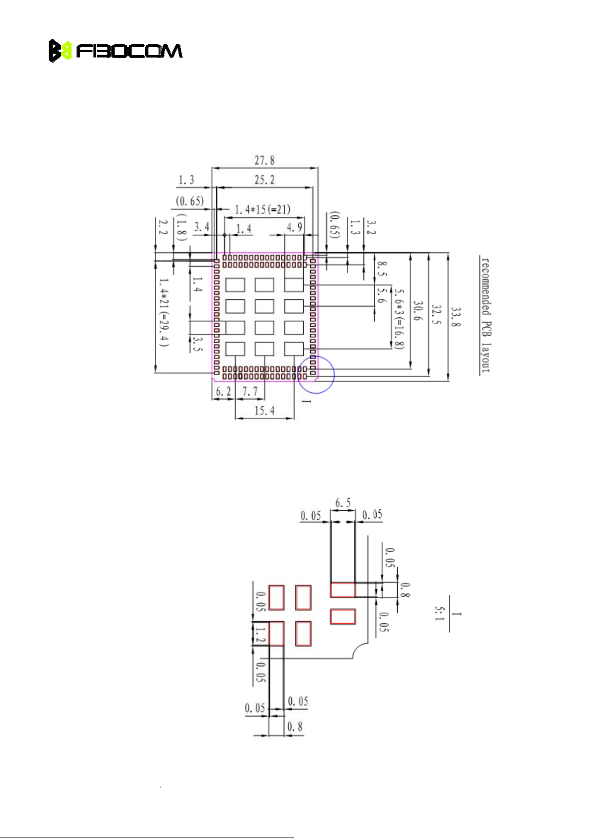
3.2 Re
ommen
PCB D
sign
H330 HSPA+
Module Hard
are User M
nual
Page 12 of 4
d
c
w
c
a
w
a
a
4
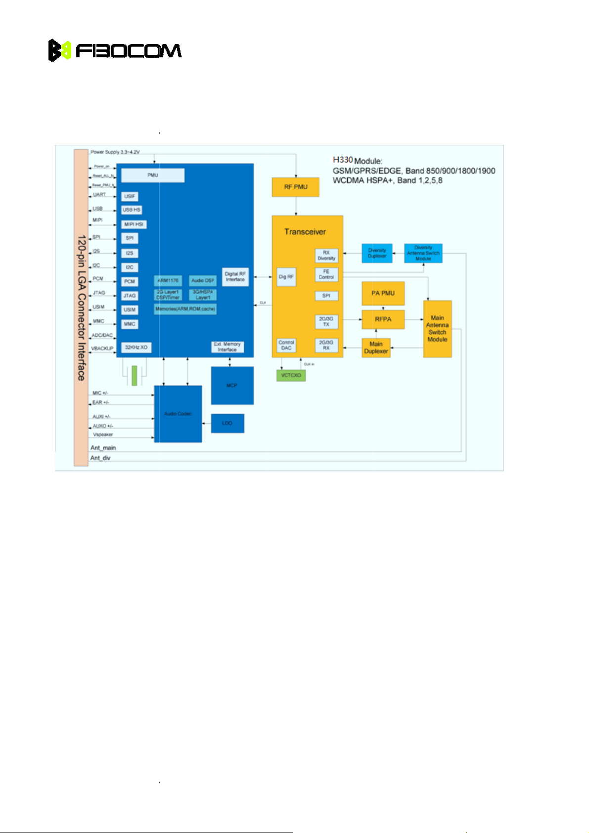
4 Har
4.1 Blo
ware S
k Diagr
ope
m
H330 HSPA+
Module Hard
are User M
nual Page 13 of 4
n
n
3
e
P
V
V
V
V
V1 V
w
o
i
c
w
a
s
t
u
u
u
t
t
t
A
t
a
A a
4
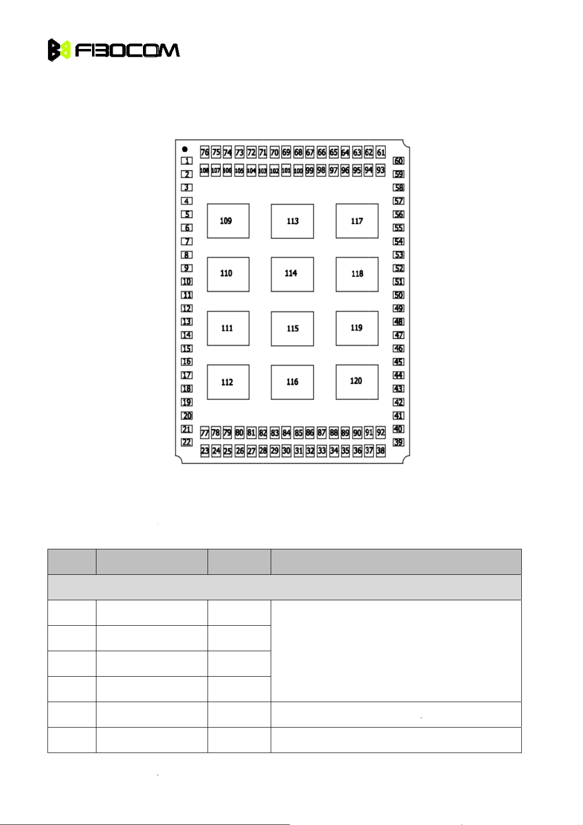
4.2 Pin
4.2.1 Pi
Definiti
Map
n
4.2.2 Pi
Notice: H3
H330 Pin d
Pin#
Power
59
60
61
62
64
Descript
0 logic ele
scription:
in Name
BAT
BAT
BAT
BAT
PA
TRX
on
trical level i
1.8V.
I/O
I
I
I
I
O
O
Descrip
Power s
Power s
Power s
ion
pply
pply indica
pply indica
or for RF P
or for RF tr
nsceiver
H330 HSPA+
Module Hard
are User M
nual
Page 14 of 4

V
V
P
P
R
U5 U6 U7 U8 U
d
U
U
A
A
E
E
M
M
A
A
A
w
F
N
L
A
w
a
o
e
o
o
s
o
s
o
a
e
e
N
e
B
B
p
p
p
p
u
u
u
u
er
o
r
4
46
47
On/off
48
49
Reset
77
USIM
4
IO
RTC
OWER_O
OWER_O
ESET_AL
SIM_CD
SIM_VCC
SIM_RST
SIM_CLK
F
_N
O
I/O
I
I
I
I
O
O
O
Digital p
Real tim
Off contr
On contr
External
USIM in
USIM p
USIM re
USIM cl
wer supply
clock pow
l signal
l signal
reset signal
ert detect, l
wer supply
et
ck
1.8V.
,1.71V ~
ow activity
1.89V
High Spee
9
10
Audio
13
14
15
16
17
18
19
SIM_DAT
SIM
SIM_D+
SIM_D-
UXO+
UXO-
AR-
AR+
IC+
IC-
UXI-
I/O
O
O
O
O
I
I
I
USIM d
High sp
High sp
Audio ch
Audio ch
Audio ch
Audio ch
Audio ch
Audio ch
Audio ch
ta
ed SIM US
ed SIM US
annel2 out
annel2 out
annel1 out
annel1 out
annel1 inp
annel1 inp
annel2 inp
data line+
data line-
ut+
ut -
ut -
ut +
t +
t -
t -
(No supp
(No suppo
rt)
t)
20
21
H330 HSPA+
UXI+
GND
Module Hard
are User M
I
GND
nual
Audio ch
Audio G
annel2 inp
D
t +。
Page 15 of 4

22
V
2
2
2
2
2
U
U
U
V
U
2
2
U
U
U
U
U
U
U
U
w
R
R
D
S
S
D
D
w
a
o
c
c
r
n
e
a
a
w
S
k
R
D
D
C
C
R
T
R
e
t
o
e
e
s
a
r
d
n
4
I2S
SPK
I
Audio c
VBAT
dec speak
r part powe
r supply, co
nect to
11 I
24 I
25 I
26 I
27 I
USB
31
32
33
34
92
I2C
S2_CLK1
S2_CLK0
S2_WA0
S2_TX
S2_RX
SB_DP
SB_DM
SB_ID
USB
SB_TEST
O
O
O
O
I
I/O
I/O
—
I
—
I2S2 clo
I2S2 clo
I2S2 wo
I2S2 tra
I2S2 rec
USB dat
USB dat
USB ID l
USB po
USB TE
k
k
d alignmen
smit line
ive line
line +
line -
ine
er supply
T line
select
28 I
29 I
UART1
35
36
37
38
39
40
41
42
UART2
C_SDA
C_SCL
ART1_RI
ART1_DS
ART1_DT
ART1_DC
ART1_CT
ART1_RT
ART1_TX
ART1_RX
I/O
O
O
I
O
O
I
O
O
I
I2C data
I2C cloc
UART1
UART1
UART1
UART1
UART1
UART1
UART1
UART1
line
line
ing indicat
TE Data S
CE Data T
arrier Dete
lear to sen
equest to
ransmitted
eceived D
t ready
rminal rea
ct
d
end
Data
ta
y
H330 HSPA+
Module Hard
are User M
nual
Page 16 of 4

U
U
A
A
W
E
H
H
A
A
D
T
C
C
S
L
N
N
N
N
w
D
D
_
_
w
a
T
R
d
d
p
S
S
p
o
o
o
o
w
a
w
n
5
o
o
r
s
r
s
w
p
p
e
m
4
45
44
ADC
50
51
EINT
56
57
USB HSIC
90
91
Antenna
ART2_TX
ART2_RX
DC2
DC1
AKE_UP
INT2
SIC_USB
SIC_USB
DATA
STRB
O
I
I
I
UART2
UART2
Analog
Analog
Wake u
External
HSIC U
HSIC U
ransmitted
eceived D
igital conve
igital conve
signal, low
interrupt, lo
B data sig
B pulse sig
Data
ta
ter 2(No
ter 1(No
activity.
activity.
al(No sup
nal(No su
upport)
upport)
ort)
port)
67
71
Other
23
53
54
55
89
86
Not Conne
73
74
NT_MAIN
NT_DIV
ACOUT
_OUT0
LKOUT0
LK32K
MI
PG
ct
C
C
I
I
I
O
Main ant
Diversity
No Sup
No supp
No supp
No supp
Sleep M
Module
enna port,
antenna p
ort
rt
rt
rt
de Indicat
ord mode i
0ohm imp
rt, 50ohm i
ndicator
dance
pedance
75
76
H330 HSPA+
C
C
Module Hard
are User M
nual
Page 17 of 4

N
N
N
N
N
N
N
N
N
N
N
N
N
N
N
N
N
N
G
G
G
G
G
G
G
w
w
4
105
106
107
108
78
79
80
81
82
83
84
85
C
C
C
C
C
C
C
C
C
C
C
C
87
88
94
95
96
101
GND
2
12
21
30
43
C
C
C
C
C
C
ND
ND
ND
ND
ND
58
63
H330 HSPA+
ND
ND
Module Hard
are User Manual
Page 18 of 4

G
G
G
G
G
G
G
G
G
G
G
G
G
G
G
G
G
G
G
G
G
G
G
G
G
G
w
w
4
65
66
68
69
70
72
93
97
98
99
100
102
ND
ND
ND
ND
ND
ND
ND
ND
ND
ND
ND
ND
103
104
109
110
111
112
113
114
115
116
117
118
ND
ND
ND
ND
ND
ND
ND
ND
ND
ND
ND
ND
119
120
H330 HSPA+
ND
ND
Module Hard
are User Manual
Page 19 of 4

d
w
A
p
l
m
t
e
r
A
w
m
w
v
m
a
p
i
e
1
d
w
h
w
f
y
n
:
ter M
3
a
e
r
a
w
n
v
p
t
s
g
e
o
p
w
a
e
d
g
3
e
m
m
m
g
e
u
o
s
r
g
c
e
a
h
s
e
r
a
h
n
r
p
c
n
g
b
a
a
e
p
c
s
e
r
r
v
t
h
e
y
H
o
H
o
m
a
p
e
t
w
r
y
g
p
y
3
e
t
e
l
w
a
R
e
s
h
s
a
c
s
4
w
r
s
e
e
5 Har
5.1 Po
5.1.1 VB
The H330
must be ab
2.0A.
It is require
Parame
VBAT
Special car
source indi
amplifier (P
transients,
ware In
er Inter
T
ower suppl
e to sustai
ent below
must be t
ectly suppli
). Therefo
ill directly
terface
ace
must be a
the voltag
in.
.6
ken when
s all the di
e, any degr
ffect the H
single exte
level durin
Re
3.8
esigning th
ital and an
adation in t
30 perform
nal DC volt
a GSM tr
ommend
power su
log interfa
e power su
ance.
ge source
nsmit burst
Max.
4.2
ply of the
es, but als
pply perfor
of 3.6V to 4
current ser
330. The si
directly su
ance, due
.2V. The po
e, which m
Unit
V
ngle extern
plies the
to losses, n
er supply
ay reach
l DC powe
F power
oises or
The burst-
from the po
transmissio
drop. If the
performanc
It is recom
H330 interf
In any case
burst. Drop
an automat
To minimiz
guidelines:
Use a
locate
Use lo
ode operat
er supply,
n bursts co
oltage dro
e.
ended that
ce connec
, the H330
ing below t
c power-off
the losses
000 uF, or
as near to
impedanc
ion of the G
which caus
sume the
s are not
the voltage
or.
upply input
he minimu
.
and transie
reater, low
the H330 in
power so
SM transmi
s tempora
ost instant
inimized, t
drops duri
must not d
operating l
nts on the
ESR capa
terface con
rce, cablin
sion and r
y voltage d
neous cur
e frequent
g a transmi
op below t
evel may r
ower suppl
itor on the
ector as p
and board
ception dr
ops of the
ent, and th
oltage fluc
burst will n
e minimum
sult in a lo
lines, it is
330 suppl
ssible.
routing.
ws instanta
ower suppl
refore caus
uations ma
ot exceed
operating l
voltage de
ecommend
inputs. Th
neous curr
y level. The
e the large
degrade t
00mV, mea
vel during
ection, whi
ed to follow
capacitor
nt surges
t voltage
e H330
ured on th
transmit
h will initiat
these
hould be
Use ca
Filter t
bling and r
e H330 su
uting as sh
ply lines u
rt as possi
ing filtering
le.
capacitors,
as describe
d in the tab
e.
H330 HSPA+
Module Hard
are User M
nual
Page 20 of 4

o
0
9
w
t
w
u
sRTC
eLow
T1 R
w
a
a
s
w
0
b
s
M
o
0
0
0
c
m
t
r
c
r
r
e
g
s
s
T522 25 29 25 2
7
4
45 2
7
4
4
6
4
s
r
4
Recom
Capacit
1000uF
10nF, 1
8.2pF, 1
33pF, 3
5.1.2 Po
Parame
I off
I idle
mended
0nF
0pF
pF
er Cons
er De
Idl
Usage
GSM Tr
Digital s
1800/19
850/900 M
mption
cription
mode
mode
nsmit curre
erge
itching noi
0 MHz GS
ands
Hz GSM ba
Conditi
Des
nt Mini
burs
e Filte
sour
Filte
nds Filte
n
ription
izes pow
s. Use max
s digital lo
es.
s transmis
s transmis
r supply lo
imum possi
ic noises f
ion EMI.
ion EMI.
ypical
3uA
0.4
ses during
ble value.
om clocks
Unit
uA
mA
transmit
and data
I sleep
I
GSM-RMS
mo
power
de
DRX
DRX
DRX
.0
.0
.0
mA
22.8
GSM85
10
PCL
15
19
7.8
8.9
4.9
29.8
GS
M voice X slot
1
x slot
EGSM9
0 PCL
10
15
19
0
8.3
5.3
4.3
152.0
mA
DCS18
H330 HSPA+
Module Hard
are User M
nual
0 PCL
5
10
8.0
7.1
Page 21 of 4

S
M
w
P
T1 R
T
R
w
a
2
0
0
0
0
0
0
0
4
6
4
4
5
2
9
5
2
90 3
9
8
3
98 4
9
5
4
PCS19
GSM85
EGSM9
0 PCL
PCL
0 PCL
15
0
5
10
15
5
10
15
19
5
10
15
5.0
150.9
8.6
7.1
4.6
65.1
13.6
105.4
1.3
83.4
17.7
105.5
I
GPRS-RM
I
EGPRS-R
G
RS Class 1
4
X slot
x slot
DCS18
PCS19
0 PCL
0 PCL
19
5
10
15
0
5
10
15
11.0
mA
53.5
167.6
5.3
6.3
73.7
174.4
100.4
1.6
88.7
EG
PRS Class
12
S
4
1
X slot
x slot
GSM85
EGSM9
PCL
0 PCL
14
19
8
14
142.4
0.9
04.7
146.9
mA
H330 HSPA+
Module Hard
are User M
nual
Page 22 of 4

M
w
aDur
C
w
a
0
0
0
0
0
0
8
92 4
92 4
9
3
9
3
9
90 95 2
90 95 2
9
4
4
DCS18
PCS19
GSM85
0 PCL
0 PCL
PCL
19
9
15
9
15
5
10
15
19
5
1.2
98.4
104.6
1.0
96.9
113.1
8.4
1556.4
50.2
120.5
1.3
1595.4
I
GSM-MAX
10
EGSM9
0 PCL
15
Pe
k current
ing TX slot
19
58.8
0.9
7.9
mA
52.9
70.6
DCS18
0 PCL
10
15
115.1
2.4
57.2
78.1
PCS19
0 PCL
10
15
24dBm
110.6
2.4
55.7
I
WCDMA-R
H330 HSPA+
W
S
Module Hard
DMA
are User M
Band5 (
nual
50)
0dBm
-24dBm
142.0
135.4
mA
Page 23 of 4

O
n
e
d
a
t
w
T
p
t
O
w
o
e
ter M
1
g
w
a
d
g
e
1
2
9
t
n
nTyp
h
0
5
5
4
b
7
o
1
a
R
U
V
4
Band2 (
Band1 (
Band8 (
900)
100)
00)
-50dBm
24dBm
0dBm
-24dBm
-50dBm
24dBm
0dBm
-24dBm
-50dBm
24dBm
0dBm
-24dBm
133.7
12.5
146.3
137.2
135.6
64.2
117.1
105.4
103.4
31.9
142.3
135.8
5.1.3 VI
The H330 i
the custom
It is for mo
digital sign
Parame
VIO @
5.1.4 VR
VRTC is a
corporates
r applicati
ule to pow
l.
orking
C
ower suppl
a regulate
n. It can be
r supply di
in.
.773
y for modul
voltage ou
used as a i
ital signal i
1.8
RTC circu
put VIO. T
dicator.
ternal H33
ical
it and can b
-50dBm
e regulator
, so it can
Max.
1.82
e connect t
134.1
provides a
e used as
external
.8V output
reference
Unit
V
TC battery.
for use by
level for
Parame
VRTC
H330 HSPA+
er
utput Volta
Module Hard
Min.
e 1.71
are User M
nual
Typical
1.8
Max.
1.89
nit
Page 24 of 4

VRTC I
n
w
n
w
e
d
e
O
n
o
n
w
e
w
t
w
e
n
r
e
e
i
n
w
a
e
o
T
d
r
S
S
S
n
n
n
VuA
n
4
(RTC is
VRTC I
(RTC is
put Voltag
orking)
put Curren
orking)
0.5
1.8
1.89
1.5
VRTC refer
Notes:
nce desig
is below:
R8 is limite
VRTC cons
C9 can det
5.2 On/
5.2.1 Pi
H330 has 3
Pin definiti
Pi
48
49
77
resistor.
umption cu
rmine the r
ff/Res
Descript
control sig
n is below:
#
rent is less
served tim
t
on
als to on,
Pin Na
POWE
POWE
RESE
than 2uA.
e.
ff ,reset mo
me
R_OFF
R_ON
_ALL_N
ule.
Elect
CMO
CMO
CMO
ical Level
1.8V
1.8V
1.8V
Descr
Off co
On co
Exter
iption
trol signal
trol signal
al reset sig
al
H330 HSPA+
Module Hard
are User M
nual
Page 25 of 4

w
H
o
r
l
w
s
w
e
a
0
:
R
w
a
e
e
o
w
a
O
r
p
i
w
e
M
h
e
R
4
5.2.2 Po
When the
H330 will p
low for a mi
Pa
Pu
Control timi
er on
330 is pow
wer on ag
nimum of 1
ameter
se width
ng is below
red off, th
in when th
0 millisec
Condition
PMU oper
POWER_
nds will tu
Min.
100
tes at low
N signal is
n H330 on
Typ
300
ower mode
falling edg
cal
, with only t
. Asserting
ax
e RTC tim
the POWE
Unit
ms
r active.
_ON signa
l
Recomman
5.2.3 Po
When
d Design:
er off
et POWE
OFF to lo
level, H33
0 will be po
er down.
H330 HSPA+
Module Hard
are User M
nual
Page 26 of 4

Pa
rPul
s
T
i
w
:
g
h
y
w
a
b
o
n
o
/
i
e
e
/
c
M
3
e
d
D
e
e
a
a
4
ameter
Condition
Min.
Typ
cal
ax
Unit
Control timi
Recomman
se width
ng is below
d Design:
100
300
000
ms
5.2.4 Re
The RESE
H330 is res
Important:
The reset s
It’s recomm
et
_N input si
et without t
gnal is ver
ended that
nal would
e work net
important f
it should co
e reset the
logging out.
r the syste
nect he 33
H330 imm
m. When d
39pF capa
diately. Wh
sign it nee
itor to GN
n the RES
be protect
on extern
ET_N sign
d totally.
l circuit.
l is low, the
H330 HSPA+
Module Hard
are User M
nual
Page 27 of 4

Pa
rPul
n
w
:
g
i
w
a
P
WVV
i
M
3
p
m
M
u
s
e
s
o
c
c
or
4
ameter
Condition
Min.
Typ
cal
ax
Unit
Control timi
Recomman
se width
ng is below
d Design:
100
300
000
ms
5.3 Indi
5.3.1 Pi
Pin#
86
89
56
1
64
H330 HSPA+
cator Si
Descript
Module Hard
nal
on
are User M
in Name
L
PG
S
MI
AKE_UP
TRX
PA
nual
Descri
Work
Sleep
Wake
Power
transc
Power
tion
ode indicat
ode Indica
p module
upply indi
iver
upply indi
tor
ator for
ator for RF
PA
Page 28 of 4

P
n
a
g
e
m
e
g
M
e
e
A
w
s
c
r
.
W
H
E
w
a
e
W
075Lo75
H
d
0
5
3
ow 5
7
n
u
S
m
e
w
t
u
f
e
o
4
5.3.2 Ind
5.3.2.1 L
LPG worki
State
• NO SIM c
• SIM Error
• Registerin
• Register n
(always)
• IDLE mod
• Calling
• Data com
• Calling Sl
icator De
G
g state des
rd
network
etwork failu
unicating
ep
cription
ription is b
e
low:
ork mode
6
0ms High,
ms High,
ms High,
igh
600ms Lo
S Low
5ms Low
Notice:Hi
5.3.2.2 S
Module
Mode
Sleep Mod
Other Mod
5.3.2.3 W
Module
Mode
Sleep
Idle/Call
h level is 1
8V.
I
SMI
2.5S
orking mo
igh; 100ms
Low
KE_UP
WAK
_UP
Low
High
Low
High
e
Low
Worki
Wake
Keep
Keep
Modul
g Descrip
p the mod
leep mode
ode, no af
cannot set
ion
le, from Sl
ect
to Sleep m
ep to Idle
de
H330 HSPA+
Module Hard
are User M
nual
Page 29 of 4

t
B
0
p
p
p
p
D
w
i
n
c
s
a
D
D
I
T
G
r
r
s
w
a
n
e
B
a
s
V
V
t
e
e
M
e
m
c
w
a
p
a
i
.
C
m
4
5.3.2.4 O
Pin Name
VTRX
VPA
Notice:
5.4 US
5.4.1 US
Pin#
31
32
her
Electr
1.8V
0-4.3V
They are i
Interfa
B Pin De
Pin N
USB_
USB_
cal Level
dicator sig
e
cription
me
P
M
Descri
RF Tra
It work
0.65
it is 0
al, it canno
I/O
I/O
I/O
ption
nsceiver P
in Tx mod
, when the
be used fo
Des
USB
USB
U work ind
, when the
ax. power
r other, it c
ription
signal +
signal -
icator
low power
it is about 4
n be set N
t is about
.3V, other
.
ode
33
34
92
H330 can s
When H33
1
2
2
2
5.4.2 US
Reference
USB_
VUSB
USB_
upport USB
connect to
ort is for 3
orts are fo
orts are fo
orts are re
B Design
esign:
D
EST
2.0. It is ne
PC by US
Modem to
AT Comm
trace.
erved.
—
I
—
d to install
, PC will g
do data op
nd.
USB
USB
USB
USB driver.
t 7 port blo
ration
ID signal
power sup
TEST sign
:
ly
l
H330 HSPA+
Module Hard
are User M
nual
Page 30 of 4

S
u
n
hpro
s
o
u
t
R
p
w
u
e
M
s
d
s
n
A
e
e
e
a
T
1
2
e
R
D
D
w
a
a
p
c
d
e
g
c
e
r
n
o
o
e
2
t
e
m
a
V
h
e
h
B
p
s
o
n
n
s
r
r
B
p
o
e
n
o
d
d
c
a
n
n
B
e
e
g
c
U
t
4
t
T101 and T
VUSB is U
Notice:
VUSB sho
USB_DP a
T
It i
po
Y
D
In
5.5 UA
5.5.1 UA
H330 sup
102 should
B power s
ld be conn
d USB_D
e layout de
tocol, with
recomme
ints on the
u don’ t ne
e to the us
erface of v
T
RT Interf
ort 2 UAR
be low cap
pply, it is 2.
ct to a level
are high s
ign of this
ifferential l
ded that s
P for debu
d to conne
d enclosur
rsion 2.0 o
ce
, one is 8 li
citor TVS, i
5V ~ 5.25V.
(2.5V ~ 5.
eed lines, i
ircuit on th
ining and i
t USB_DP
.
t the USB_
material, t
higher. Th
es ; the ot
t is below 1
5V) or US
is 480 Mb
AP board
pedance c
nd USB_D
BUS whe
e mobile p
connectio
er is 2 line
pF.
cannot be
s, It is PC
hould com
ntrol to 90
M pins as t
the functio
one shall
to so calle
。
ecognized.
Layout req
ly with the
hm.
st points a
of USB is
nly be con
power US
uirement b
USB 2.0 hi
d then pla
not used.
ected to a
is prohibi
low:
h speed
e these tes
SB
ed.
8 l
2 l
UART1
ines UART
ines UART
and UART
support fl
only supp
2 defined b
w control, c
rt AT
low:
an be used
to downloa
or AT com
munication.
UART1
Pin#
35
36
37
H330 HSPA+
Pin Nam
UART1_
UART1_
UART1_
Module Hard
I
SR
TR
are User M
I/O
O
I
O
nual
Desc
UART
UART
UART
iption
1 Ring indi
1 DTE Data
1 DCE Dat
ator
Set ready
Terminal r
ady
Page 31 of 4

E
i
E
i
w
D
C
R
T
R
e
R
T
n
c
U
c
U
w
a
P
P
,
r
,
r
r
2
2
d
d
e
e
o
e
e
b
3
b
3
(
(
4
38
39
40
41
42
UART2
Pin#
44
45
5.5.2 UA
H330(DC
Appl
UART1_
UART1_
UART1_
UART1_
UART1_
Pin Nam
UART2_
UART2_
RT Desig
)UART1
cation MC
CD
TS
TS
XD
XD
XD
XD
onnect to
(DTE)
O
I
O
O
I
I/O
I
O
C(DTE)
Signal di
UART
UART
UART
UART
UART
Desc
UART
UART
the signal
ection
1 Carrier D
1 Clear to s
1 Request t
1 Transmitt
1 Received
iption
Transmitt
Received
irection is
H3
tect
nd
send
d Data
Data
d Data
Data
elow:
0 Module
DCE)
RXD
TXD
RTS
CTS
DSR
DTR
RI
DCD
H330(DC
Appl
)UART2
cation MC
onnect to
(DTE)
C(DTE)
Signal di
the signal
ection
UA
UA
UA
UA
UA
UA
UA
UA
irection is
H3
RT1_TXD
RT1_RXD
RT1_CTS
RT1_RTS
RT1_DTR
RT1_DSR
RT1_RI
RT1_DCD
elow:
0 Module
DCE)
RXD
TXD
UA
RT2_TXD
UA
RT2_RXD
H330 HSPA+
Module Hard
are User M
nual
Page 32 of 4

Notice:
T
o
t
M
s
I
P567814
I
d
w
i
n
e
M
c
n
w
a
e
s
C
S
L
O
D
i
g
O
O
.
p
o
e
o
a
r
s
s
s
4
H330 UAR
If DTE is n
When use i
5.6 USI
H330
5.6.1 US
high level
t suitable,
, need car
upport USI
M Interfa
in#
s 1.8V.
eed add el
about the
,now don’
e
Pin Nam
USIM_V
USIM_R
USIM_C
USIM_I
ctrical level
ignal direct
t support hi
e I/
C O
T O
K O
I/
translation
on.
h speed SI
M.
Descri
USIM p
USIM R
USIM cl
USIM d
tion
wer supply
set signal
ck signal
ta signal
output
5.6.2 US
Reference
2
M Desig
esign:
GND
USIM_C
G
ND
I
USIM g
USIM in
ound
ert detect
ignal
H330 HSPA+
Module Hard
are User M
nual
Page 33 of 4

I
t
e
h
h
c
h
e
D
w
D
n
s
n
f
d
s
d
r
n
s
w
a
p
d
r
a
a
e
m
e
e
n
3
p
m
m
g
d
u
c
y
e
c
S
a
a
o
g
d
c
E
a
y
p
E
d
e
e
h
c
l
t
S
a
e
E
a
n
s
e
m
n
f
a
R
S
d
e
r
a
T
f
a
o
8
s
4
a
Notice:
5.6.3 US
The SIM in
card. There
meets the r
T
so
T
co
To
re
USIM_IO
USIM_C
M Desig
erface and
are several
quired sta
e SIM shou
urces, such
e SIM inter
nnector an
avoid cros
ommende
is pulled u
can suppo
Notice
ignals desi
design gui
dards and
ld be locate
as the RF
ace signals
the SIM tr
talk betwe
to rout the
internal H
rt SIM hot
gn is extre
elines that
egulations.
d, and its si
ntenna an
length sho
y. This is to
n the SIM
separatel
30.
lug, low is
ely import
ust be foll
nals shoul
digital swit
ld not exce
meet with
lock and d
on the ap
ctive and S
nt for prop
wed to ac
be routed,
hing signa
ed 100 mm
MC regula
ta signals (
lication bo
IM card is i
r operation
ieve a robu
away from
s.
between th
ions and i
IM_CLK a
rd, and pre
serted。
of H330 an
t and stabl
any possibl
H330 inte
prove sign
d SIM_DA
erably isol
the SIM
design th
e EMI
face
l integrity.
A), it is
ted by a
t
su
rrounding g
T
el
(T
e SIM card
ments (ze
K). We al
ound plan
signals sho
er diodes,
o recomme
.
uld be prot
tc.). The re
ded the E
cted from
ommende
D compon
SD using v
part no of
nt should l
ry low cap
SD is AV
yout with
citance pr
-M1005C0
IM hold clo
tective
0MTAAB
ely.
H330 HSPA+
Module Hard
are User M
nual
Page 34 of 4

I
o
a
i
e
I
o
AT
t
o
a
n
a
o
w
u
p
W
s
=
t
M
S
u
g
i
c
o
m
w
a
n
n
n
o
M
c
e
8
S
a
g
H
r
e
m
h
M
8
P
t
e
e
o
0
l
p
c
o
o
o
o
o
o
o
o
w
M
m
,
s
n
o
o
o
o
e
d
e
n
r
u
d
r
l
4
5.6.4 US
H330 supp
5.6.4.1 H
When SIM
In referenc
When no S
5.6.4.2 S
When set
detected wi
SIM_CD=L
SIM_CD=H
Important:
disabled co
M Hot Pl
rt SIM hot
rdware De
s removed,
design US
M card, S
ftware De
+MSMPD
h SIM_CD
w level, SI
igh or NC,
The defa
rrespondin
g
lug.
sign
USIM_CD i
IM_CD con
2 is high; I
ign
1, the SIM
pin.
card is o
IM card is
lt value of
ly.
s high; inse
ect U3 Pin
sert SIM,
detected fe
site and re
ff site and
SMPD pa
rt SIM ,USI
(SW2),
W2 connec
ture will b
ister the n
330 drop
ameter is “
_CD is lo
in7(SW1
SW1,USI
actives. Th
twork auto
ut the netw
”. And also
。
) connect
_CD is pull
e SIM card
atically.
ork.
the SIM d
GND.
ed down。
is on site o
tected feat
not will be
re was
5.7 An
5.7.1 Pi
The H330
interface's
fully control
commands
Pin#
13
14
15
16
17
log Aud
Descript
udio interfa
perating m
led by the h
set.
Pin Na
AUXO+
AUXO-
EAR-
EAR+
MIC+
io
on
e supports
des, activ
ost applicat
e
two chann
devices, a
ion, throug
I/O
O
O
O
O
I
l audio dev
plification
advanced
Des
Audi
Audi
Audi
Audi
Audi
ices and op
evels and
rogrammi
ription
channel2
channel2
channel1
channel1
channel1 i
erating mo
peech proc
g options a
utput+
utput -
utput -
utput +
nput +
es. The au
ssing algo
d a versati
io
ithms are
e AT
18
19
20
H330 HSPA+
MIC-
AUXI-
AUXI+
Module Hard
are User M
I
I
I
nual
Audi
Audi
Audi
channel1 i
channel2 i
channel2 i
nput -
nput -
nput +。
Page 35 of 4

d
u
B
u
c
c
e
e
c
e
t
e
u
c
c
m
v
w
n
W
e
n
t
n
m
A
w
a
a
W
e
d
h
n
m
n
d
n
A
c
d
d
a
e
I
d
i
c
p
d
i
V
o
o
V
n
d
h
d
e
e
w
n
u
a
a
e
o
e
p
d
x
x
e
m
e
n
BKo
n
p
h
4
21
22
5.7.2 Au
The au
Spurious s
In PC
performanc
5.7.2.1 A
Audio
Audio
Param
Bias vo
AGND
VSPK
io Descr
dio input a
ppression.
Layout, th
e, the input
dio Chan
hannel 1 in
hannel 1:
ters
ltage
iption
d output ch
hen conn
differential
and output
el 1
terface are
MIC input c
Test co
No load
GND
I
nnels are
ct to the h
lines need
need GND
ifferential l
aracteristi
ditions
Audi
Audi
to
ifferential i
ndset, nee
qual lengt
solation an
nes, Can b
:
Min
1.9
GND
codec spe
BAT
terfaces. A
external a
, parallel, a
the interfa
use as H
Typ
2.0
aker part p
d have pre
dio amplifi
s short as
ce need ad
nd-phone.
Ma
2.1
wer supply,
fect perfor
r.
ossible, for
ESD prot
U
V
connect
ance at RF
a better
ction.
it
Gain
Load r
Audio
Param
Out vol
Load r
DC Bia
5.7.2.2 A
Audio
Note:
sistance
hannel 1:
ters
age
sistance
s voltage
dio Chan
hannel 2 in
The VSPK
Program
gain:2dB
EAR output
Test co
No load
el 2
terface are
ust be co
able,ste
characteris
ditions
ifferential l
nected to
s
0
tic:
Min
nes, Can b
BAT, Other
2.2
Typ
32
1
use as H
ise it will b
nd-free.
outwork.
32
Ma
2
d
U
V
o
V
hm
it
p
m
Audio
Para
Bias
H330 HSPA+
hannel 2:
eters
oltage
Module Hard
UXI input
Test con
No load
are User M
haracterist
itions
nual
ic:
Min
1.9
Typ
2.0
Max
2.1
Unit
V
Page 36 of 4

Gain
r
c
m
o
r
a
i
w
A
o
w
a
m
A
u
n
e
K
0
A
0
p
r
s
C
rSer
M
R
p
u
u
4
Program
gain:2dB
able,ste
s
0
32
dB
Load
Audio
Para
Out v
Load
DC Bi
5.8 Dig
Pin#
24
25
esistance
hannel 2:
eters
ltage
esistance
s voltage
tal Audi
UXO outp
Test co
No load
Pin Nam
I2S2_CL
I2S2_WA
t characte
istic:
ditions
I/O
0 O
O
Min
De
cription
Bit
lock
Fra
me clock(L
2.2
Typ
8
2
Max
4
CK)
Kohm
Unit
Vpp
ohm
V
26
27
28
29
54
I2S2_TX
I2S2_RX
I2C_DAT
I2C_SCL
CLKOUT
O
I
I/O
O
O
Se
ial data out
ial data inp
I2C
data line
I2C
clock line
26
Hz clock o
ut
t
tput
H330 HSPA+
Module Hard
are User M
nual
Page 37 of 4

C
I
I
K
e
a
w
s
o
5
e
p
w
a
m
z
G
v
(
z
、
A
H
1
4
5.8.1 I2S
5.8.2 I2
Notice:
(1)
(2)
5.9 Oth
Other
2S can be
t support s
Hz, 11.02
r
re not sup
et master
me audio s
KHz, 8 KH
orted like
ode of sla
ample rate
).
PIO、MIPI
er mode
48KHz, 44.
MMC、D
1KHz, 32K
C now.
z, 24 KHz,
22.5 KHz,
6 KHz, 12
H330 HSPA+
Module Hard
are User M
nual
Page 38 of 4

t
c
s
n
v
s
a
u
u
w
n
h
t
n
r
C
w
a
r
h
t
c
n
.
n
4
6 Elec
6.1 Ele
The table i
VBAT
Digital Sig
6.2 En
The table i
Operation
Temperat
Storage
Temperat
rical a
trical C
H330 elec
al
ironme
H330 envi
l
re
re
d Envir
aracter
rical charac
Min.
-0.2
-0.2
tal Cha
onmental c
ondition
onmen
istic
teristic:
acteristi
aracteristi
Mi
-30
-40
al
c
:
.
Max
4.2
1.9
Max.
+85
+85
U
V
V
it
Unit
°C
°C
H330 HSPA+
Module Hard
are User M
nual
Page 39 of 4

n
m
n
t
e
a
S
S
S
S
v
a
S
S
S
S
w
e
u
S
t
n
n
w
a
n
A
M
.
t
8
1
M
8
1
7
9
2
9
6
9
6
4
7 RF I
H330
Main a
Diversi
7.1 Op
7.1.1 Ma
Oper
UMT
UMT
UMT
UMT
GSM
terfac
odule incl
tenna:G
y antenna:
rational
in Antenn
ting Band
2100 (Ban
1900 (Ban
850 (Ba
900 (Ba
850 MHz
des main a
M/WCDM
WCDMA d
Band
a
d I IMT)
d II PCS)
d V CLR)
d VIII GS
tenna and
Tx and Rx
iversity Rx
)
diversity an
.
Tx
1920–19
1850–19
824–849
880–915
824–849
enna.
0 MHz
0 MHz
Hz
MHz
Rx
2110–
1930–1
869–8
925–9
869–8
170 MHz
990 MHz
4 MHz
0 MHz
4 MHz
GSM
GSM
GSM
7.1.2 Di
Oper
UMT
UMT
UMT
UMT
900
1800(DCS)
1900(PCS)
ersity
ting Band
2100 (Ban
1900 (Ban
850 (Band
900 (Band
d I IMT)
d II PCS)
V CLR)
VIII GSM)
880–915
1710–17
1850–19
Rx
2110–21
1930–19
869–894
925–960
MHz
5 MHz
0 MHz
0 MHz
0 MHz
MHz
MHz
925–9
1805–1
1930–1
0 MHz
880 MHz
990 MHz
H330 HSPA+
Module Hard
are User M
nual
Page 40 of 4

y
g
r
m
p
p
e
n
f
d
w
e
e
i
m
w
5
s
c
d
a
t
y
S
w
a
t
<
e
e
s
e
s
r
h
u
d
d
d
m
e
e
w
a
h
o
e
o
y
d
w
e
e
4
m
n
w
。
t
c
e
a
f
c
e
d
a
e
f
a
h
e
t
a
s
h
4
e
e
RF PCB
7.1.3 La
When desi
The shorte
It is recom
Add a π-ty
Design
out Guid
n RF, we n
the better,
ended to
e circuit (t
line
ed connec
nsert loss
ount H330
o parallel d
H330 mod
0.2dB,an
module an
vice groun
le RF pin t
impedanc
antenna c
pin directl
antenna,
is 50ohm.
nnector to
to the mai
e recomm
he same si
n land) for
nded to us
e of layout
ntenna ma
micro-line
.
ching.
7.1.4 Im
All RF lines
should be
7.2 Ant
7.2.1 Ma
1. Anten
Antenna ef
The radiate
losses: retu
dimensions
2. S11 or
S11 (return
in Antenn
a Efficien
iciency is th
rn loss, ma
.
VSWR
loss) indica
edance
nna De
power of
Efficienc
0ohm imp
ign
a Design
y
e ratio of th
n antenna
erial loss, a
of the ma
tes the deg
dance。
Require
input pow
is always lo
nd coupling
ter antenn
ee to whic
ent
r to the ra
er than th
loss. The
> 40% (–
the input i
iated or re
input pow
fficiency of
dB)
pedance o
eived powe
due to th
n antenna
an antenn
r of an ante
following
relates to it
matches t
nna.
ntenna
electrical
e referenc
impedance
H330 HSPA+
(50 ohm).
Module Hard
11 shows t
are User M
e resonanc
nual
e feature a
d impedan
e bandwidt
of an ante
na. Voltag
Page 41 of 4

a
e
z
a
p
o
o
n
n
a
o
s
e
t
e
r
e
p
I
T
w
S
o
e
a
a
n
f
f
m
a
f
s
m
e
a
C
a
t
t
r
d
0
0
0
w
a
o
<
h
m
a
d
m
m
a
n
a
e
u
t
n
s
s
0
s
o
e
m
n
s
n
e
e
o
s
r
h
C
1
.
c
n
e
e
r
o
n
r
d
Y
n
s
c
e
t
h
e
e
e
o
o
e
Y
k
e
t
n
l
s
,
a
e
t
e
n
s
n
m
o
e
e
r
t
s
e
4
n
n
a
n
e
o
d
standing w
be measur
S11 o
3. Polari
The polariz
direction of
The linear
antenna 。
4. Radiat
The radiati
The radiati
PIFA anten
A
R
5. Gain a
ve ratio (V
d with vect
f the mast
ation
tion of an
maximum r
olarizatio
ion Pattern
n pattern o
n pattern o
a is recom
tenna area
diation P
nd Directiv
WR) is an
r analyzer.
r antenna
ntenna is t
diation。
is recom
an antenn
half wave
ended:
:high
6m
ttern :o
ity
ther expre
–10 dB
e orientati
ended for
reflects th
ipole anten
*wide 10
nidirectio
sion of S11
n of the ele
the anten
radiation f
nas is the b
m*long 1
al
S11 relate
tric field v
a:diversi
atures of t
st for wirel
00mm
。
to the ant
ctor that ro
y antenna
e antenna i
ss termina
nna efficie
ates with ti
different t
the remot
ls. If it is bui
cy. S11 ca
e in the
main
field regio
lt-in antenn
.
,
The radiati
all direction
6. Interfe
Besides th
(especially
sources on
sources, su
interferenc
can be dec
reduce the
LCD with o
or design fil
7. TRP/T
TRP (
n pattern o
。
Reco
rence
antenna p
he TIS) of t
the user bo
ch as the L
signals th
eased due
ffects of in
timized pe
ter circuits.
S
otal Radiate
an antenn
mended a
rformance,
he module.
rd must b
D, CPU, a
t affect the
o interfere
erference
formance;
Power
):
represent
tenna gai
the interfer
To guarant
properly c
dio circuit
normal ope
ce signals.
ources on t
hield the L
the field st
≤ 2.5dBi.
nce on the
e high perf
ntrolled. O
, and powe
ation of the
Therefore,
e module.
D interfere
ength of th
user board
rmance of
the user b
supply. All
module. F
uring the d
ou can ta
ce signals;
radiated e
also affect
the module
ard, there
the interfer
r example,
sign, you
e the follow
shield the
ectromagn
the radio p
the interfe
re various
nce source
he module
eed to con
ing measur
ignal cable
tic waves i
erformance
ence
interferenc
s emit
sensitivity
ider how t
s: Use an
of the boar
;
W850/W
GSM85
GSM90
DCS180
H330 HSPA+
Module Hard
900/W190
>27dBm
>28dBm
>25dBm
are User M
/W2100>
nual
9dBm
Page 42 of 4

TIS (
o
v
s
n
n
e
n
M
u
t
m
h
d
3
o
w
0
W
0
0
0
t
g
r
C
T
s
b
n
a
t
a
m
w
w
a
d
0
m
m
0
i
f
a
a
D
f
e
s
C
a
n
a
e
m
i
a
e
n
n
a
d
C
a
e
o
g
o
s
e
s
r
C
o
m
a
y
a
a
o
r
l
n
u
-
a
r
e
u
c
e
t
e
d
u
n
H
/
a
w
a
p
n
t
4
F
PCS190
T
tal Isotropic
W850/W
>25dBm
Sensitivity
900<-102
):
Bm
7.2.2 Di
H330 diver
Diversity a
Main anten
EU Reg
Hereby, Sh
compliance
/W1900/
GSM85
GSM90
DCS180
ersity an
ity antenna
tenna desi
a and dive
ulatory
nzhen G&
with the es
2100<-1
<-102dB
<-102dB
/PCS190
enna des
is optical, I
n methods
sity antenn
onform
Industrial
ential requ
3dBm;
<-102dB
gn
need to su
and the ma
isolation r
nce
evelopme
irements an
pport diver
n antenna,
quirement
t Co., Ltd.,
d other rele
ity, must to
its efficienc
greater th
declares th
vant provisi
increase th
indicators
n 12dB.
t this mod
ns of Dire
diversity a
to allow the
le, model
tive 1999/5
ntenna.
lower 3dB.
330 is in
EC.
Importa
The H330
H330 Mod
conditions.
1. At leas
all times.
2. To co
radiation, t
exceed 2.5
3. The H
transmitter
t compl
odule has
le in their fi
Otherwise,
20cm sep
ply with FC
e maximu
Bi.
30 Module
r antenna
iance in
een grant
al product
dditional F
ration dist
C regulatio
antenna g
and its ant
ithin a hos
ormatio
d modular
without ad
C approv
nce betwe
s limiting b
in includin
nna must n
t device.
for No
pproval for
itional FC
ls must be
n the anten
th maximu
cable loss
t be co-loc
th Ame
mobile app
certificatio
btained.
a and the
RF outpu
in a mobile
ted or ope
ican us
ications. In
if they me
ser’s body
t power an
only expos
ating in co
rs
egrators m
t the follo
must be m
human ex
re conditio
junction wi
y use the
ing
intained at
osure to R
must not
h any other
H330 HSPA+
Module Hard
are User M
nual
Page 43 of 4

e
o
S
C
r
w
f
r
h
t
e
n
w
a
o
o
t
o
d
C
h
c
w
d
y
r
0
m
u
e
c
c
F
s
e
c
r
p
a
e
o
s
r
e
C
f
e
n
d
n
T
4
o
4. A label
with a state
must be af
ment simila
5. A user
manual wit
that must b
The end pr
emission te
duct with a
sting requir
Note: If this
satisfy the
module is i
AR require
FCC NOTI
Changes o
E:
modificatio
observed
ixed to the
to the follo
the end pr
o ensure c
n embedde
ments and
tended for
ments of F
ns made to
utside of t
wing: For H
duct must
mpliance
H330 Mo
be properl
use in a po
C Part 2.1
this equip
e end prod
330: This d
learly indi
ith current
ule may al
authorized
table devic
93.
ent not exp
ct into whi
vice contai
ate the ope
CC RF ex
o need to p
per FCC P
, you are r
essly appr
h the H330
ns FCC ID:
ating requi
osure guid
ass the FC
rt 15.
sponsible
ved by Sh
Module is i
ZMOH330.
ements an
lines.
Part 15 u
or separate
nzhen G&
corporated
conditions
intentional
approval t
Industrial
,
Developme
nt Co., Ltd.
may void th
e FCC auth
orization to
operate thi
equipment
.
H330 HSPA+
Module Hard
are User M
nual
Page 44 of 4
 Loading...