Fairchild Semiconductor MM74HC123ASJ, MM74HC123ASJX, MM74HC123AN, MM74HC123AM, MM74HC123AMTC Datasheet
...
September 1983
Revised February 1999
MM74HC123A Dual Retriggerable Monostable Multivibrator
© 1999 Fairchild Semiconductor Corporation DS005206.prf www.fairchildsemi.com
MM74HC123A
Dual Retriggerable Monostable Multivibrator
General Description
The MM74HC123A high spe ed monostable multivibrato rs
(one shots) utilize advanced silicon-gate CMOS technology. They feature speeds comparab le to low p ower S chottky TTL circuitry while retaining the low p ower and high
noise immunity characteristic of CMOS circuits.
Each multivibrator fea tures b oth a n egative , A, a nd a po sitive, B, transition trigg ered input, either of which can be
used as an inhibit input. Also includ ed is a clear input that
when taken low resets t he one shot. The MM74HC123A
can be triggered on the positive transition of the clear while
A is held LOW and B is held HIGH.
The MM74HC123A is retri ggerable. That i s it may be triggered repeatedly while their outputs are generating a pulse
and the pulse will be extended.
Pulse width stability over a wide range of temperature and
supply is achieved using linear CMOS techniques. The out-
put pulse equation is s imply: PW = (R
EXT
) (C
EXT
); where
PW is in seconds, R is in ohms, and C is in farads. All
inputs are protected from dam age due to static discharge
by diodes to V
CC
and ground.
Features
■ Typical propagation delay: 25 ns
■ Wide power supply range: 2V–6V
■ Low quiescent current: 80 µA maximum (74HC Series)
■ Low input current: 1 µA maximum
■ Fanout of 10 LS-TTL loads
■ Simple pulse width formula T = RC
■ Wide pulse range: 400 ns to ∞ (typ)
■ Part to part variation: ±5% (typ)
■ Schmitt Trigger A & B inputs enab le infinite signa l input
rise and fall times.
Ordering Code:
Devices also availab le in Tape and Reel. Specify by appending th e s uffix let t er “X” to the ordering cod e.
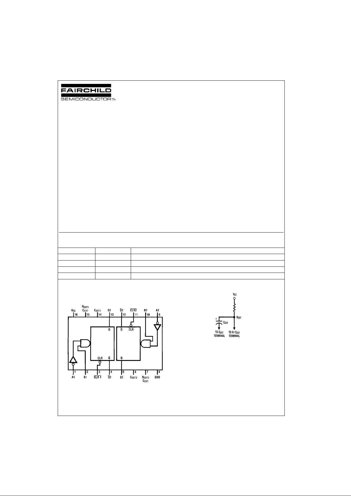
Connection Diagram
Pin Assignment for DIP, SOIC, SOP and TSSOP
Top View
Timing Component
Note: Pin 6 and Pin 14 must be ha rd-wired to GND.
Order Number Package Number Package Description
MM74HC123AM M16A 16-Lead Small Outline Integrated Circuit (SOIC), JEDEC MS-012, 0.150” Narrow
MM74HC123ASJ M16D 16-Lead Small Outline Package (SOP), EIAJ TYPE II, 5.3mm Wide
MM74HC123AMTC MTC16 16-Lead Thin Shrink Small Outline Package (TSSOP), JEDEC MO-153, 4.4mm Wide
MM74HC123AN N16E 16-Lead Plastic Dual-In-Line Package (PDIP), JEDEC MS-001, 0.300” Wide

www.fairchildsemi.com 2
MM74HC123A
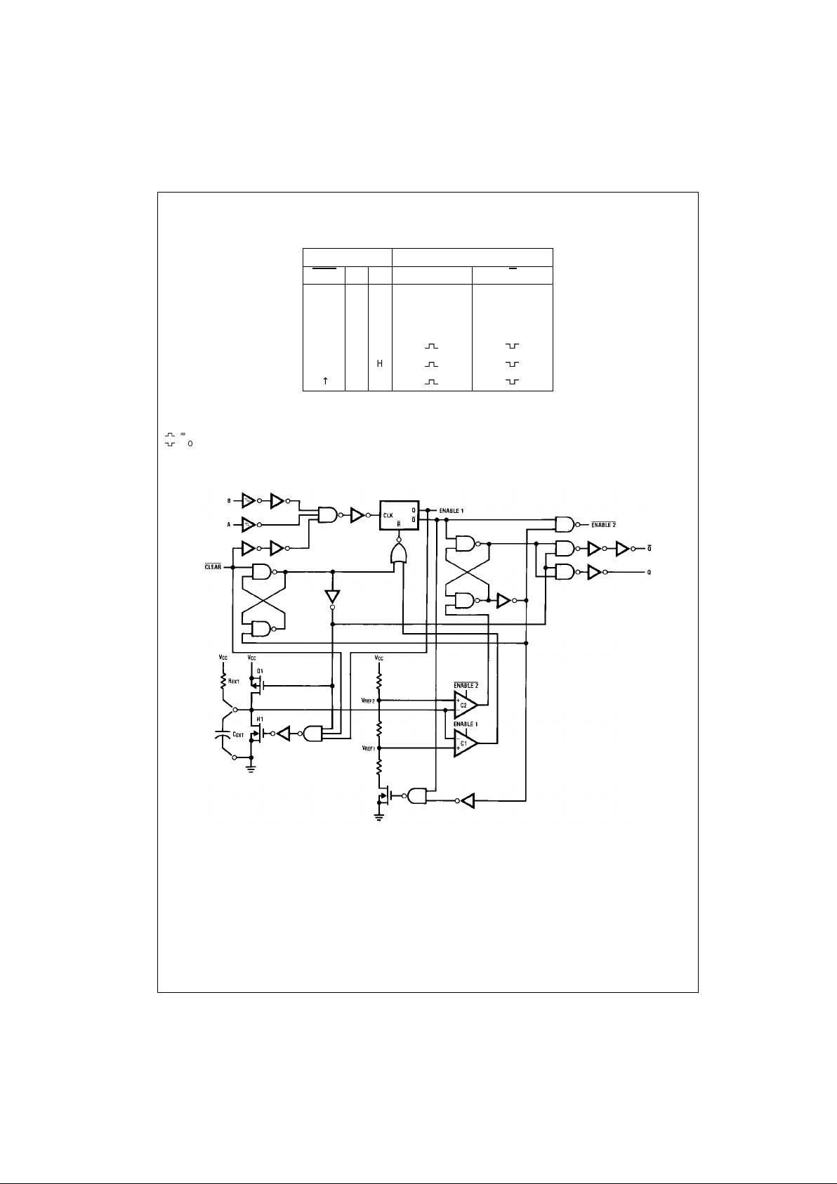
Truth Table
H = HIGH Level
L = LOW Level
↑=Transition from LOW-to-HIGH
↓=Transition from HIGH-to-LOW
= One HIGH Level Pulse
= One LOW Level Pulse
X = Irrelevant
Logic Diagram
Inputs Outputs
Clear
AB Q Q
LXX L H
XHX L H
XXL L H
HL↑
H ↓ H
↑ LH

3 www.fairchildsemi.com
MM74HC123A
Absolute Maximum Ratings(Note 1)
(Note 2)
Recommended Operating
Conditions
Note 1: Maximum Ratings are those values beyond which damage to the
device may occur.
Note 2: Unless otherwise specified all voltages are referenced to ground.
Note 3: Power Dissipation Temperature Derating: Plast ic “N” Package: −
12mW/°C from 65°C to 85°C
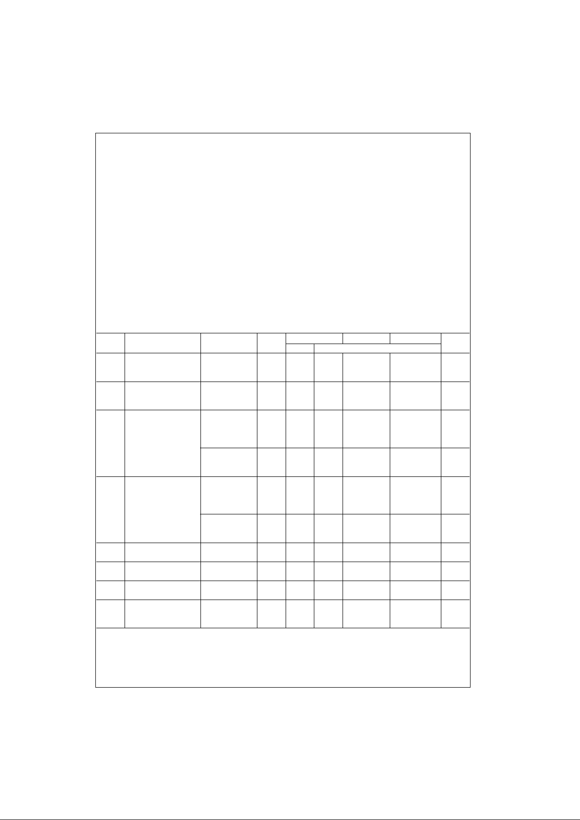
DC Electrical Characteristics (Note 4)
Note 4: For a power supply of 5V ±10% the worst-case output voltages (VOH, VOL) occur for HC at 4.5V. Thus the 4.5V values should be us ed w hen design-
ing with this supply. Worst-case V
IH
and VIL occur at V
CC
= 5.5V and 4.5V resp ec t iv ely. (The VIH value at 5.5V is 3.85V.) The worst-cas e leakage current
(I
IN
, ICC, and IOZ) occur for CMOS at the higher voltage and s o t he 6.0V values should be used.
Supply Voltage (VCC) −0.5V to +7.0V
DC Input Voltage (V
IN
) −1.5V to V
CC
+1.5V
DC Output Voltage (V
OUT
) −0.5V to V
CC
+0.5V
Clamp Diode Current (I
IK
, IOK) ±20 mA
DC Output Current, per pin (I
OUT
) ±25 mA
DC V
CC
or GND Current, per pin (ICC) ±50 mA
Storage Temperature Range (T
STG
) −65°C to +150°C
Power Dissipation (P
D
)
(Note 3) 600 mW
S.O. Package only 500 mW
Lead Temperature (T
L
)
(Solderi ng 10 seconds) 260°C
Min Max Units
Supply Voltage (V
CC
)26V
DC Input or Output Voltage 0 V
CC
V
(V
IN
, V
OUT
)
Operating Temperature Range (T
A
) −40 +85 °C
Input Rise or Fall Times
(Clear Input)
(t
r
, tf)V
CC
= 2.0V 1000 ns
V
CC
= 4.5V 500 ns
V
CC
= 6.0V 400 ns
Symbol Parameter Conditions
V
CC
TA = 25°CTA = −40 to 85°CTA = −55 to 125°C
Units
Typ Guaranteed Limits
V
IH
Minimum HIGH Level Input 2.0V 1.5 1.5 1.5 V
Voltage 4.5V 3.15 3.15 3.15 V
6.0V 4.2 4.2 4.2 V
V
IL
Maximum LOW Level Input 2.0V 0.3 0.3 0.3 V
Voltage 4.5V 0.9 0.9 0.9 V
6.0V 1.2 1.2 1.2 V
V
OH
Minimum HIGH Level V
IN
= VIH or V
IL
Output Voltage |I
OUT
| ≤ 20 µA 2.0V 2.0 1.9 1.9 1.9 V
4.5V 4.5 4.4 4.4 4.4 V
6.0V 6.0 5.9 5.9 5.9 V
V
IN
= VIH or V
IL
V
|I
OUT
| ≤ 4.0 mA 4.5V 4.2 3.98 3.84 3.7 V
|I
OUT
| ≤ 5.2 mA 6.0V 5.7 5.48 5.34 5.2 V
V
OL
Maximum LOW Level V
IN
= VIH or V
IL
Output Voltage |I
OUT
| ≤ 20 µA 2.0V 0 0.1 0.1 0.1 V
4.5V 0 0.1 0.1 0.1 V
6.0V 0 0.1 0.1 0.1 V
V
IN
= VIH or V
IL
V
|I
OUT
| ≤ 4 mA 4.5V 0.2 0.26 0.33 0.4 V
|I
OUT
| ≤ 5.2 mA 6.0V 0.2 0.26 0.33 0.4 V
I
IN
Maximum Input Current V
IN
= VCC or GND 6.0V ±0.5 ±5.0 ±5.0 µA
(Pins 7, 15)
I
IN
Maximum Input Current V
IN
= VCC or GND 6.0V ±0.1 ±1.0 ±1.0 µA
(all other pins)
I
CC
Maximum Quiescent Supply V
IN
= VCC or GND 6.0V 8.0 80 160 µA
Current (standby) I
OUT
= 0 µA
I
CC
Maximum Active Supply VIN= VCC or GND 2.0V 36 80 110 130 µA
Current (per R/C
EXT
= 0.5V
CC
4.5V 0.33 1.0 1.3 1.6 mA
monostable) 6.0V 0.7 2.0 2.6 3.2 mA
 Loading...