www.fairchildsemi.com
ML6553
Bus Termination Regulator
Features
• Can source and sink up to 1A
• Generates termination voltages for DDR SDRAM,
SSTL_2 SDRAM, SGRAM, or equivalent memories
• Generates termination voltages for active termination
schemes for GTL+, DDR, Rambus
™
, VME, LV-TTL,
PECL and other high speed logic
•V
regulated to within 3% at 800mA
L
• Minimum external components. Requires no feedback
compensation
• Fixed frequency operation for easier system integration
• Lower power consumption than passive, resistor divider
termination, reducing heat by as much as 50%
• Separate voltages for V
CCQ
and PV
DD
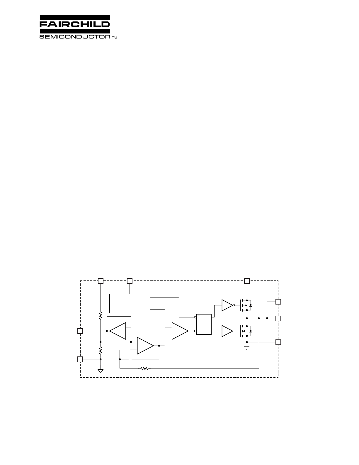
Block Diagram
General Description
The ML6553 switching regulator is designed to convert
voltage supplies ranging from 2.0V to 3.6V into a desired
output voltage or termination voltage for various applications. The ML6553 can be implemented to produce
regulated output voltages in two different modes. In the
default mode, the output is 50% of voltage applied to V
The switching regulator is capable of sourcing or sinking up
to 1A of current.
The ML6553, used in conjunction with series termination
resistors, provides an excellent voltage source for active
termination schemes of high speed transmission lines as
those seen in high speed memory buses and distributed backplane designs. The voltage output of the regulator can be
used as a termination voltage for other bus interface
standards such as SSTL, DDR, Rambus
™
, GTL+, VME,
LV-CMOS, LV-TTL, P-ECL, and CMOS.
CCQ
.
V
2
AGND
3
190kΩ
CCQ/2
1
V
CCQ
OSCILLATOR/
RAMP GENERATOR
BUFFER
190kΩ
4
AV
CC
CLK
RAMP
SRQ
–
+
V
INTEG
+
–
–
+
PWM
COMPARATOR
Q
5
PV
DD
V
L
Q1
Q2
6
V
L
7
DGND
8
REV. 1.0.2 3/21/01

ML6553 PRODUCT SPECIFICATION
Pin Configuration
ML6553
8-Pin SOIC (S08)
DGND
V
V
CCQ/2
AGND
AV
CCQ
CC
1
2
3
4
TOP VIEW
8
V
7
L
V
6
L
PV
5
DD
Pin Description
Pin Name Function
1V
2V
CCQ
CCQ/2
3 AGND Analog signal ground
4AV
5PV
6V
7V
CC
DD
L
L
8 DGND Return for the internal power transistors.
Voltage supply for internal reference voltage divider
V
output is V
REF
CCQ/2
Voltage supply for the noise sensitive analog control section.
Voltage supply for the internal power transistors.
Output inductor connection
Output inductor connection
Absolute Maximum Ratings
Absolute maximum ratings are those values beyond which the device could be permanently damaged. Absolute maximum
ratings are stress ratings only and functional device operation is not implied.
Parameter Min. Max. Unit
V
IN
Voltage on Any Other Pin GND – 0.3 V
Peak Switch Current (I
Average Switch Current (I
)1A
PEAK
) 300 mA
AVG
5V
+ 0.3 V
IN
Junction Temperature 150 °C
Storage Temperature Range –65 150 °C
Lead Temperature (Soldering, 10 sec) 150 °C
Thermal Resistance ( θ
) 160 °C/W
JA
Output Current, Source or Sink 1 A
Operating Conditions
Temperature Range 0°C to 70°C
AV
, PV
CC
Operating Range 2.0V to 3.6V
DD
2
REV. 1.0.2 3/21/01

PRODUCT SPECIFICATION ML6553
Electrical Characteristics
AV
= PV
CC
Symbol Parameter Conditions Min Typ Max Units
Switching Regulator
V
TT
V
CCQ/2
I
REF
Supply
I
Q
= 3.3V ±10%. Unless otherwise specified, T
DD
Output Voltage, V
TT
(See Figure 2) V
Output Voltage, V
Source Resistance from V
CCQ/2
L
I
OUT
REF
I
OUT
V
REF
Note 2 V
= Operating Temperature Range (Note 1)
A
= 0, V
= open V
= ±1A, V
= open V
= 2.3V 1.12 1.15 1.18 V
CCQ
= 2.5V 1.22 1.25 1.28 V
CCQ
V
= 2.7V 1.32 1.35 1.38 V
CCQ
= 2.3V 1.09 1.15 1.21 V
CCQ
= 2.5V 1.19 1.25 1.31 V
CCQ
= 2.7V 1.28 1.35 1.42 V
CCQ
V
= 2.3V 1.139 1.15 1.162 V
CCQ
V
= 2.5V 1.238 1.25 1.263 V
CCQ
V
= 2.7V 1.337 1.35 1.364 V
CCQ
20 m Ω
Switching Frequency 650 kHz
Output Load Current for V
CCQ/2
3mA
Pin
Quiescent Current I
= 0, no load I
OUT
VCCQ
I
AVCC
IPV
DD
10 µA
500 µA
4.5 mA
Notes:
1. Limits are guaranteed by 100% testing, sampling, or correlation with worst-case test conditions.
2. Specifications are taken from the application circuit in Figure 2 using the recommended component values.
REV. 1.0.2 3/21/01
3
 Loading...