

Fairchild Semiconductor ML4827-2 Datasheet
www.fairchildsemi.com
REV. 1.0.1 6/27/01
Features
• Pin-compatible with industry-standard ML4824-1
• TriFault Detect™ to conform to UL1950™ requirements
• Available in 50% or 74% max duty cycle versions
• Low total harmonic distortion
• Reduces ripple current in the storage capacitor between
the PFC and PWM sections
• Average current, continuous boost leading edge PFC
• High efficiency trailing-edge PWM can be configured for
current mode or voltage mode operation
• Average line voltage compensation with brown-out
control
• PFC overvoltage comparator eliminates output
“runaway” due to load removal
• Current fed gain modulator for improved noise immunity
• Overvoltage protection, UVLO, and soft start
General Description
The ML4827 is a controller for power factor corrected,
switched mode power supplies, that includes circuitry
necessary for conformance to the safety requirements of
UL1950. A direct descendent of the industry-standard
ML4824-1, the ML4827 adds a TriFault Detect™ function to
guarantee that no unsafe conditions may result from single
component failure in the PFC. Power Factor Correction
(PFC) allows the use of smaller, lower cost bulk capacitors,
reduces power line loading and stress on the switching FETs,
and results in a power supply that fully complies with
IEC1000-3-2 specification. The ML4827 includes circuits
for the implementation of a leading edge, average current,
“boost” type power factor correction and a trailing edge,
pulse width modulator (PWM). The device is available in
two versions; the ML4827-1 (Duty Cycle
MAX
= 50%) and
the ML4827-2 (Duty Cycle
MAX
= 74%). The higher
maximum duty cycle of the -2 allows enhanced utilization of
a given transformer core’s power handling capacity. An overvoltage comparator shuts down the PFC section in the event
of a sudden decrease in load. The PFC section also includes
peak current limiting and input voltage brown-out
protection. The PWM section can be operated in current or
voltage mode, and includes a duty cycle limit to prevent
transformer saturation.
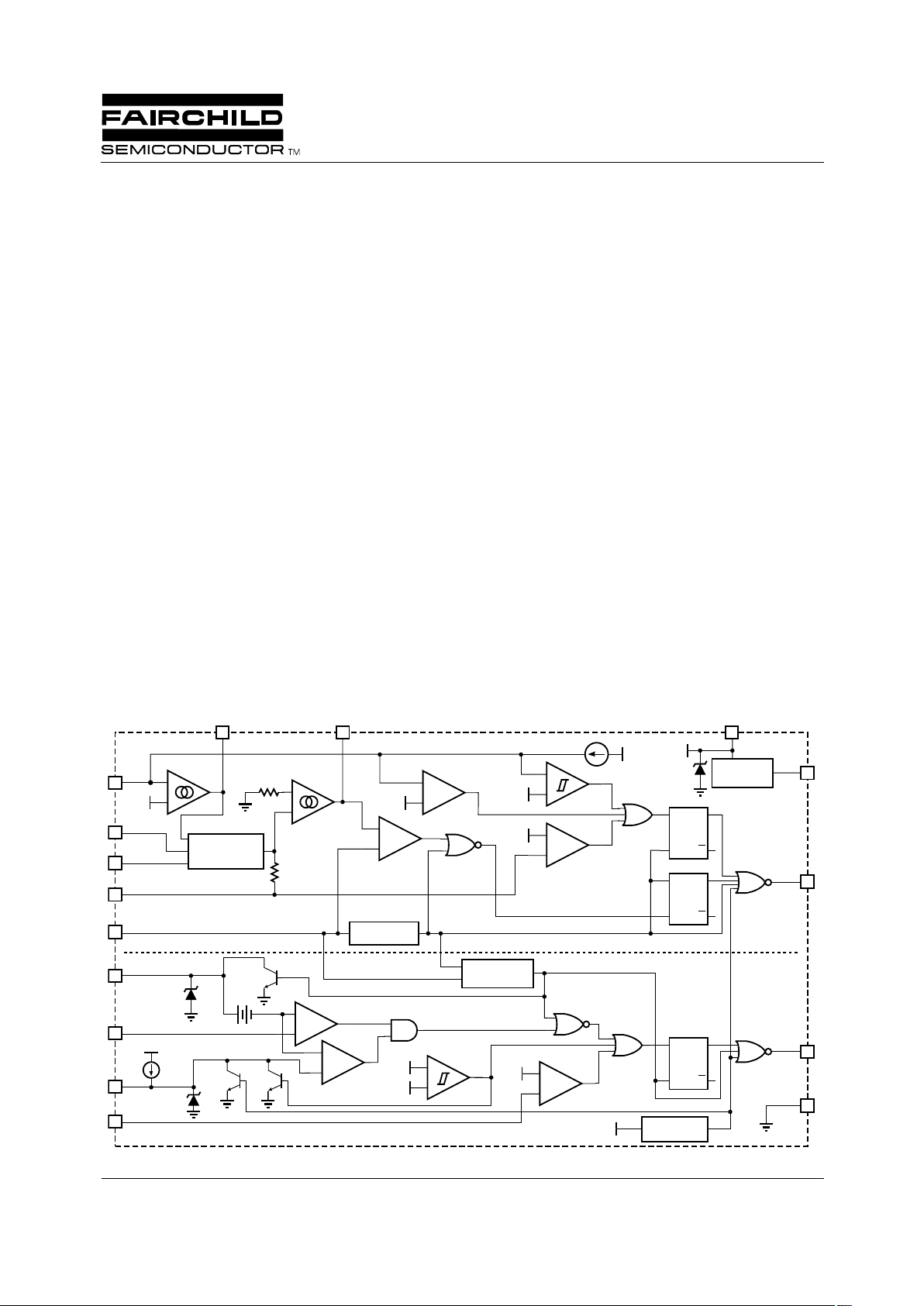
Block Diagram
VEAO IEAO
V
FB
I
AC
V
RMS
I
SENSE
RAMP 1
OSCILLATOR
OVP
PFC I
LIMIT
UVLO
V
REF
PULSE WIDTH MODULATOR
POWER FACTOR CORRECTOR
BROKEN WIRE
COMPARATOR
2.5V
+
–
–
+
7.5V
REFERENCE
V
CC
V
CCZV
REF
VEA
+
–
IEA
+
–
+
–
+
–
PFC OUT
SRQ
Q
SRQ
Q
2.7V
–1V
0.5V
2µA
RAMP 2
PWM OUT
SRQ
Q
V
DC
SS
DC I
LIMIT
V
CC
DUTY CYCLE
LIMIT
–
+
1V
–
+
2.5V
V
FB
–
+
8V
8V
VIN OK
GAIN
MODULATOR
V
CCZ
3.5kΩ
3.5kΩ
1.25V
50µA
–
+
13.5V
DC I
LIMIT
14
12
11
GND
10
15
2
4
3
7
8
6
5
9
16 1 13
ML4827
Fault-Protected PFC and PWM Controller Combo
ML4827 PRODUCT SPECIFICATION
2 REV. 1.0.1 6/27/01
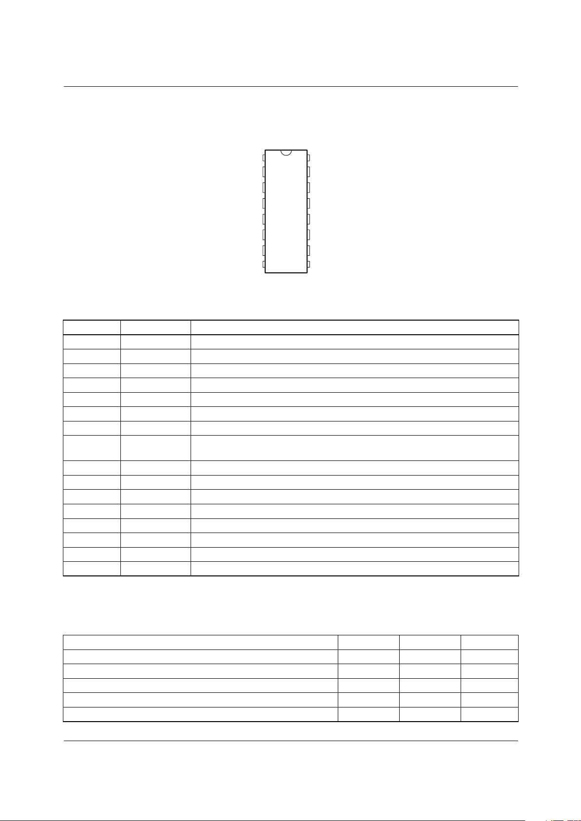
Pin Configuration
Pin Description
Absolute Maximum Ratings
Absolute Maximum Ratings are those values, beyond which the device could be permanently damaged. Absolute maximum
ratings are stress ratings only and functional device operation is not implied.
PIN NAME FUNCTION
1 IEAO PFC transconductance current error amplifier output
2IACPFC gain control reference input
3I
SENSE
Current sense input to the PFC current limit comparator
4V
RMS
Input for PFC RMS line voltage compensation
5 SS Connection point for the PWM soft start capacitor
6VDCPWM voltage feedback input
7 RAMP 1 PFC (master) oscillator input; f
OSC
set by RTC
T
8 RAMP 2 When in current mode, this pin functions as as the current sense input; when in
voltage mode, it is the PWM (slave) oscillator input.
9 DC I
LIMIT
PWM current limit comparator input
10 GND Ground
11 PWM OUT PWM driver output
12 PFC OUT PFC driver output
13 V
CC
Positive supply (connected to an internal shunt regulator)
14 V
REF
Buffered output for the internal 7.5V reference
15 V
FB
PFC transconductance voltage error amplifier input, and TriFault Detect input
16 VEAO PFC transconductance voltage error amplifier output
Parameter Min. Max. Units
V
CC
Shunt Regulator Current 55 mA
I
SENSE
Voltage –35 V
Voltage on any other Pin GND-0.3 V
CCZ +0.3
V
I
REF
20 mA
IAC Input Current 10 mA
1
2
3
4
5
6
7
8
16
15
14
13
12
11
10
9
IEAO
I
AC
I
SENSE
V
RMS
SS
V
DC
RAMP 1
RAMP 2
VEAO
V
FB
V
REF
V
CC
PFC OUT
PWM OUT
GND
DC I
LIMIT
TOP VIEW
ML4827
16-Pin PDIP (P16)
16-Pin Wide SOIC (S16W)
PRODUCT SPECIFICATION ML4827
REV. 1.0.1 6/27/01 3
Operating Conditions
Electrical Characteristics
Unless otherwise specified, ICC = 25mA, RT = 21.8kΩ, CT = 1000pF, TA = Operating Temperature Range (Note 1)
Peak PFC OUT Current, Source or Sink 500 mA
Peak PWM OUT Current, Source or Sink 500 mA
PFC OUT, PWM OUT Energy Per Cycle 1.5 µJ
Junction Temperature 150 °C
Storage Temperature Range –65 150 °C
Lead Temperature (soldering, 10s) 260 °C
Thermal Resistance (θ
JA
)
Plastic DIP
Plastic SOIC
80
105
°C/W
°C/W
Parameter Min. Max. Units
Temperature Range
ML4827CP, CS
ML4827IP, IS
0
–40
70
85
°C
°C
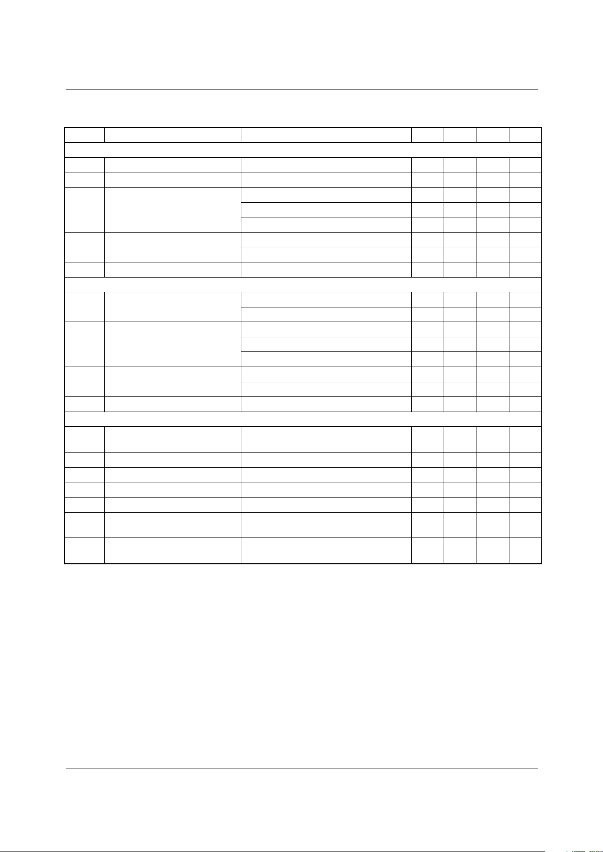
Symbol Parameter Conditions Min. Typ. Max. Units
Voltage Error Amplifier
Input Voltage Range 0 7 V
Transconductance V
NON INV
= V
INV
, VEAO = 3.75V 50 85 120 µΩ
Feedback Reference Voltage 2.48 2.55 2.62 V
Input Bias Current Note 2 –1 –2µA
Output High Voltage 6.0 6.7 V
Output Low Voltage 0.6 1.0 V
Source Current ∆VIN = ±0.5V, V
OUT
= 6V –40 –80 µA
Sink Current ∆VIN = ±0.5V, V
OUT
= 1.5V 40 80 µA
Open Loop Gain 60 75 dB
Power Supply Rejection Ratio V
CCZ
- 3V < VCC < V
CCZ
- 0.5V 60 75 dB
Current Error Amplifier
Input Voltage Range –1.5 2 V
Transconductance V
NON INV
= V
INV
, VEAO = 3.75V 130 195 310 µΩ
Input Offset Voltage 2 10 17 mV
Input Bias Current –0.5 –1.0 µA
Output High Voltage 6.0 6.7 V
Output Low Voltage 0.6 1.0 V
Source Current ∆VIN = ±0.5V, V
OUT
= 6V –40 –90 µA
Sink Current ∆VIN = ±0.5V, V
OUT
= 1.5V 40 90 µA
Open Loop Gain 60 75 dB
Power Supply Rejection Ratio V
CCZ
- 3V < VCC < V
CCZ
- 0.5V 60 75 dB
OVP Comparator
Threshold Voltage 2.6 2.7 2.8 V
Hysteresis 80 115 150 mV
Ω
Ω
ML4827 PRODUCT SPECIFICATION
4 REV. 1.0.1 6/27/01
Tri-Fault Detect
Fault Detect HIGH 2.6 2.7 2.8 V
Time to Fault Detect HIGH V
FB
= V
FAULT DETECT LOW
to VFB =
OPEN 1nF from V
FB
to GND
12ms
Fault Detect LOW 0.4 0.5 0.6 V
PFC I
LIMIT
Comparator
Threshold Voltage –0.8 –1.0 –1.15 V
∆(PFC I
LIMIT VTH
- Gain
Modulator Output)
100 190 mV
Delay to Output 150 300 ns
DC I
LIMIT
Comparator
Threshold Voltage 0.9 1.0 1.1 V
Input Bias Current ±0.3 ±1 µA
Delay to Output 150 300 ns
VIN OK Comparator
Threshold Voltage 2.45 2.55 2.65 V
Hysteresis 0.8 1.0 1.2 V
Gain Modulator
Gain (Note 3) IAC = 100µA, V
RMS
= VFB = 0V 0.36 0.55 0.66
IAC = 50µA, V
RMS
= 1.2V, VFB = 0V 1.20 1.80 2.24
IAC = 50µA, V
RMS
= 1.8V, VFB = 0V 0.55 0.80 1.01
IAC = 100µA, V
RMS
= 3.3V, VFB = 0V 0.14 0.20 0.26
Bandwidth IAC = 100µA 10 MHz
Output Voltage IAC = 250µA, V
RMS
= 1.15V, VFB = 0V 0.74 0.82 0.90 V
Oscillator
Initial Accuracy TA = 25°C 75 80 85 kHz
Voltage Stability V
CCZ
- 3V < VCC < V
CCZ
- 0.5V 1 %
Temperature Stability 2 %
Total Variation Line, Temp 72 88 kHz
Ramp Valley to Peak Voltage 2.5 V
Dead Time PFC Only 450 600 750 ns
CT Discharge Current V
RAMP 2
= 0V, V
RAMP 1
= 2.5V 4.5 7.5 9.5 mA
Reference
Output Voltage TA = 25°C, I(V
REF
) = 1mA 7.4 7.5 7.6 V
Line Regulation V
CCZ
- 3V < VCC < V
CCZ
- 0.5V 2 10 mV
Load Regulation 1mA < I(V
REF
) < 20mA 2 15 mV
Temperature Stability 0.4 %
Total Variation Line, Load, Temp 7.35 7.65 V
Long Term Stability TJ = 125°C, 1000 Hours 5 25 mV
Symbol Parameter Conditions Min. Typ. Max. Units
Electrical Characteristics (Continued)
ML4827 PRODUCT SPECIFICATION
5 REV. 1.0.1 6/27/01
Notes:
1. Limits are guaranteed by 100% testing, sampling, or correlation with worst-case test conditions.
2. Includes all bias currents to other circuits connected to the V
FB
pin.
3. Gain = K x 5.3V; K = (I
GAINMOD
- I
OFFSET
) x IAC x (VEAO - 1.5V)-1.
PFC
Minimum Duty Cycle V
IEAO
> 4.0V 0 %
Maximum Duty Cycle V
IEAO
< 1.2V 90 95 %
Output Low Voltage I
OUT
= –20mA 0.4 0.8 V
I
OUT
= –100mA 0.8 2.0 V
I
OUT
= 10mA, VCC = 8V 0.7 1.5 V
Output High Voltage I
OUT
= 20mA 10 10.5 V
I
OUT
= 100mA 9.5 10 V
Rise/Fall Time CL = 1000pF 50 ns
PWM
Duty Cycle Range ML4827-1 0-44 0-47 0-50 %
ML4827-2 0-64 0-70 0-74 %
Output Low Voltage I
OUT
= -20mA 0.4 0.8 V
I
OUT
= -100mA 0.8 2.0 V
I
OUT
= 10mA, VCC = 8V 0.7 1.5 V
Output High Voltage I
OUT
= 20mA 10 10.5 V
I
OUT
= 100mA 9.5 10 V
Rise/Fall Time CL = 1000pF 50 ns
Supply
Shunt Regulator Voltage
(V
CCZ
)
12.8 13.5 14.2 V
V
CCZ
Load Regulation 25mA < ICC < 55mA ±100 ±300 mV
V
CCZ
Total Variation Load, Temp 12.4 14.6 V
Start-up Current VCC = 11.8V, CL = 0 0.7 1.0 mA
Operating Current VCC < V
CCZ
- 0.5V, CL = 0 16 19 mA
Undervoltage Lockout
Threshold
12 13 14 V
Undervoltage Lockout
Hysteresis
2.7 3.0 3.3 V
Symbol Parameter Conditions Min. Typ. Max. Units
Electrical Characteristics (Continued)
 Loading...