

Fairchild Semiconductor ML4823 Datasheet
May 1997
ML4823
High Frequency Power Supply Controller
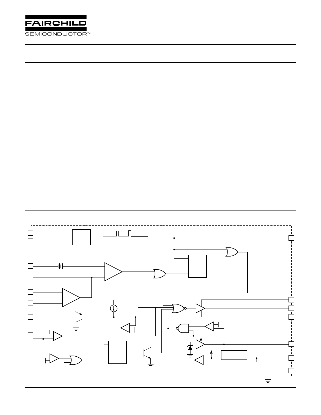
GENERAL DESCRIPTION
The ML4823 High Frequency PWM Controller is an IC
controller optimized for use in Switch Mode Power
Supply designs running at frequencies to 1MHz.
Propagation delays are minimal through the comparators
and logic for reliable high frequency operation while slew
rate and bandwidth are maximized on the error amplifier.
This controller is designed for single-ended applications
using voltage or current mode and provides for input
voltage feed forward.
A 1V threshold current limit comparator provides cycleby-cycle current limit and exceeding a 1.4V threshold
initiates a soft-start cycle. The soft start pin doubles as a
maximum duty cycle clamp. All logic is fully latched to
provide jitter-free operation and prevent multiple pulsing.
An under-voltage lockout circuit with 800mV of hysteresis
assures low startup current and drives the outputs low
during fault conditions.
FEATURES
■ Practical operation at switching frequencies to 1.0MHz
■ High current (2A peak) totem pole output
■ Wide bandwidth error amplifier
■ Fully latched logic with double pulse suppression
■ Pulse-by-pulse current limiting
■ Soft start and max. duty cycle control
■ Under voltage lockout with hysteresis
■ 5.1V trimmed bandgap reference
■ Low start-up current (1.1mA)
■ Pin compatible improved replacement for UC3823
■ Fast shut down path from current limit to output
■ Soft start latch ensures full soft start cycle
■ Outputs pull low for undervoltage lockout
This controller is an improved second source for the
UC3823 controller; however, the ML4823 includes
features not found on the 3823. These features are set in
italics.
BLOCK DIAGRAM (Pin Configuration Shown for 16-Pin Version)
R
5
C
6
RAMP
7
E/A OUT
3
NI
2
INV
1
SOFT START
8
I
LIM
11
I
LIM
9
1.4V
T
+
+
ERROR
AMP
–
OSC
+
COMP
–
R
S
V+
R
Q
S
–
–
+
1V
5.1V
Q
UNDER
VOLTAGE
LOCKOUT
–
+
+
ENABLE
V
REF
V
REF
9V
4V
GEN
INTERNAL
BIAS
T
1.25V
REF
–
/S.D.
+
+
–
CLOCK OUT
POWER V
OUTPUT
POWER GND
5.1V V
REF
V
CC
SIGNAL GND
4
C
13
14
12
16
15
10
REV. 1.0 10/12/2000
ML4823
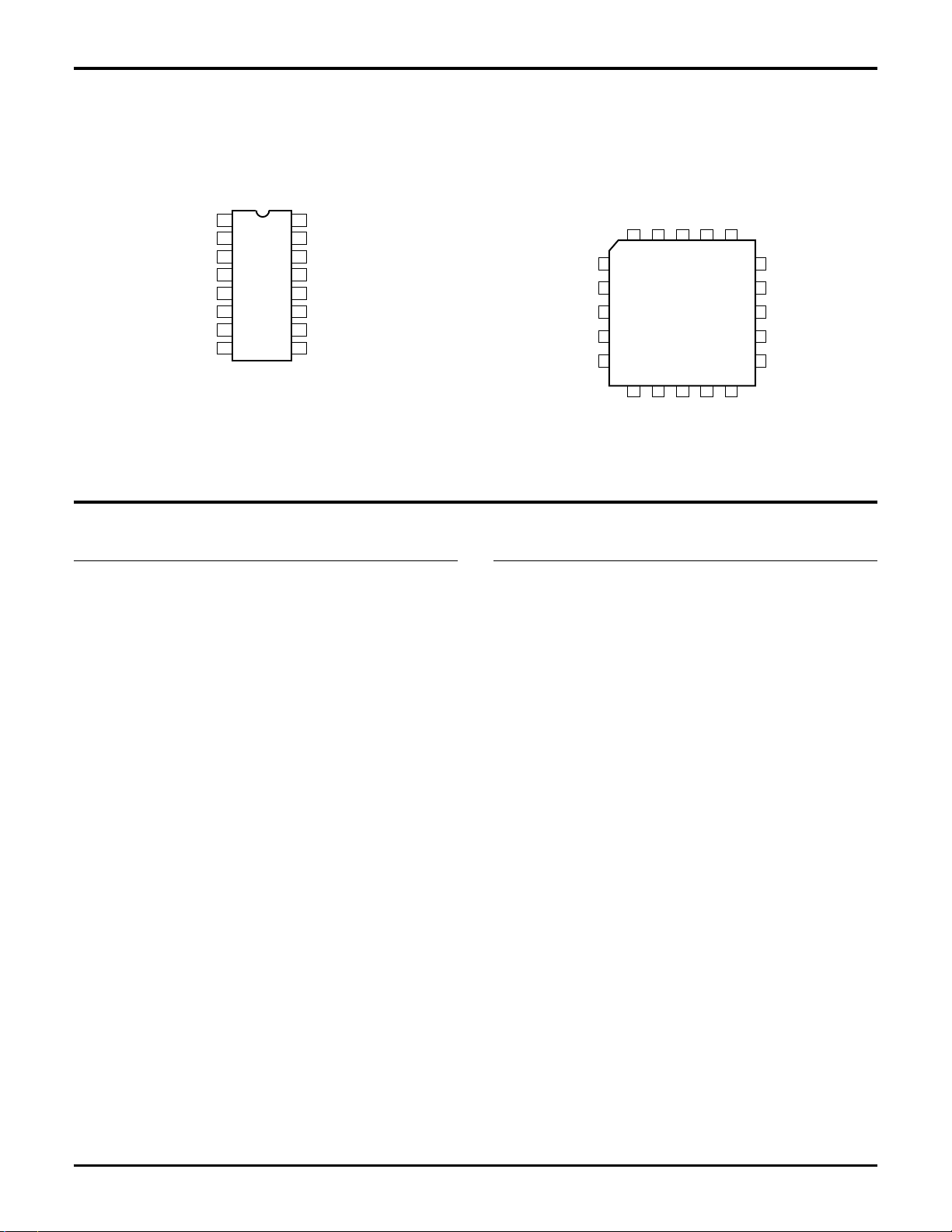
PIN CONFIGURATION
ML4823
16-PIN DIP (P16)
ML4823
20-PIN PLCC (Q20)
16-PIN SOIC (S16W)
INV
E/A OUT
CLOCK
RAMP
1
NI
2
3
4
R
5
T
C
6
T
7
SS
8
TOP VIEW
5.1V REF
16
V
15
CC
OUTPUT
14
V
13
C
PWR GND
12
I
LIM
GND
I
LIM
REF
/S.D.
11
10
9
E/A OUT
CLOCK
NC
C
R
T
T
NI
INV
3212019
4
5
6
7
8
910111213
SS
RAMP
TOP VIEW
PIN DESCRIPTION (Pin Numbers in Parentheses are for PLCC Version)
PIN NAME FUNCTION PIN NAME FUNCTION
1 (2) INV Inverting input to error amp.
2 (3) NI Non-inverting input to error amp.
3 (4) E/A OUT Output of error amplifier and input to
main comparator.
4 (5) CLOCK Oscillator output.
5 (7) R
T
Timing resistor for oscillator — sets
charging current for oscillator timing
capacitor (pin 6).
6 (8) C
T
Timing capacitor for oscillator.
7 (9) RAMP Non-inverting input to main
comparator. Connected to C
T
for
Voltage mode operation or to current
sense resistor for current mode.
8 (10) SS Normally connected to soft start
capacitor.
9 (12) I
10 (13) GND Analog signal ground.
11 (14) I
12 (15) PWR GND Return for the high current totem
13 (17) V
14 (18) OUT B High current totem pole output.
15 (19) V
16 (20) 5.1V REF Buffered output for the 5.1V voltage
/S.D. Current limit sense pin. Normally
LIM
connected to current sense resistor.
REF Reference input for cycle-by-cycle
LIM
current limit comparator.
pole output.
C
Positive supply for the high current
totem pole output.
CC
Positive supply for the IC.
reference.
NC
NC
CC
5.1V REF
V
/S.D.
GND
LIM
I
18
17
16
15
14
OUTPUT
V
C
NC
PWR GND
REF
I
LIM
2 REV. 1.0 10/12/2000

ABSOLUTE MAXIMUM RATINGS
ML4823
Absolute maximum ratings are those values beyond which
the device could be permanently damaged. Absolute
maximum ratings are stress ratings only and functional
device operation is not implied.
Supply Voltage (V
, VCC) ...........................................30V
C
OUTPUT Current, Source or Sink
DC .......................................................................0.5A
Junction Temperature ............................................ 125°C
Storage Temperature Range ..................... –65°C to 150°C
Lead Temperature (Soldering 10 sec.) .................... 260°C
Thermal Resistance (θ
)
JA
Plastic DIP .......................................................80°C/W
Plastic SOIC................................................... 105°C/W
Plastic Chip Carrier (PLCC) .............................. 78°C/W
Pulse (0.5µs) ......................................................... 2.0A
Analog Inputs
(INV, NI, RAMP, SS, I
).................. GND –0.3V to 6V
LIM
CLOCK OUTPUT Current ...................................... –5mA
F/A OUT Current ......................................................5mA
SOFT START Sink Current....................................... 20mA
RT Charging Current ............................................... –5mA
OPERATING CONDITIONS
Temperature Range
ML4823C ..................................................0°C to 70°C
ML4823I................................................ –40°C to 85°C
ELECTRICAL CHARACTERISTICS
Unless otherwise specified, R
PARAMETER CONDITIONS MIN TYP MAX UNITS
OSCILLATOR
Initial Accuracy TJ = 25°C, 360 400 440 kHz
Voltage Stability 10V ≤ VCC ≤ 30V, 0.2 2 %
Temperature Stability 5%
Total Variation Line, temp. 340 460 kHz
Clock Out High 3.9 4.5 V
Clock Out Low 2.3 2.9 V
Ramp Peak 2.6 2.8 3.0 V
Ramp Valley 0.7 1.0 1.25 V
Ramp Valley to Peak 1.6 1.8 2.0 V
REFERENCE
Output Voltage TJ = 25°C, IO = 1mA 5.025 5.10 5.175 V
Line Regulation 10V ≤ VCC ≤ 30V 2 20 mV
Load Regulation 1mA ≤ IO ≤ 10mA 5 20 mV
Temperature Stability –40°C ≤ TJ ≤ 150°C, 0.2 0.4 %
Total Variation Line, load, temp. 4.975 5.225 V
Output Noise Voltage 10Hz to 10kHz 50 µV
Long Term Stability TJ = 125°C, 1000 hrs, 5 25 mV
Short Circuit Current V
ERROR AMPLIFIER
Input Offset Voltage ±30 mV
Input Bias Current 0.6 3 µA
Input Offset Current 0.1 1 µA
Open Loop Gain 1 ≤ VO ≤ 4V 50 95 dB
= 3.65kΩ, C
T
= 1000pF, TA = Operating Temperature Range, VCC = 15V. (Note 1)
T
= 0V –15 –50 –100 mA
REF
REV. 1.0 10/12/2000 3
 Loading...