Fairchild Semiconductor MCT9001 Datasheet

8
1
8
1
8
1
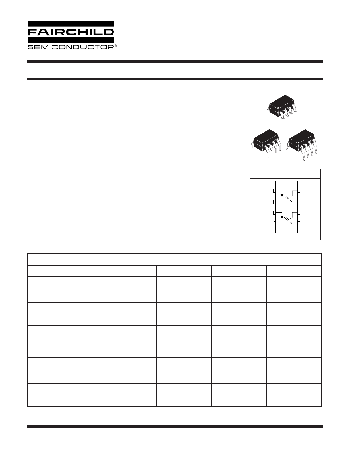
SCHEMATIC
COLLECTOR
EMITTER
ANODE
CATHODE
1
2
3
4 5
6
7
8
EMITTER
COLLECTOR
CATHODE
ANODE
Equivalent Circuit
DUAL PHOTOTRANSISTOR
OPTOCOUPLERS
MCT9001
DESCRIPTION
The MCT9001 Optocoupler has two channels for density applications. For four
channel applications, two-packages fit into a standard 16-pin DIP socket. Each
channel is an NPN silicon planar phototransistor optically coupled to a gallium
arsenide infrared emitting diode.
FEATURES
•Two isolated channels per package
•Two packages fit into a 16 lead DIP socket
• Underwriters Laboratory (U.L.) recognized File E90700
APPLICATIONS
•AC Line/Digital Logic - isolate high voltage transients
• Digital Logic/Digital Logic - Eliminate spurious grounds
• Digital Logic/AC Triac Control - isolate high voltage transients
•Twisted pair line receiver - Eliminate ground loop feedthrough
•Telephone/Telegraph line receiver - isolate high voltage transients
• High Frequency Power Supply Feedback Control - Maintain floating grounds and
transients
• Relay contact monitor - isolate floating grounds and transients
•Power supply monitor - Isolate transients
ABSOLUTE MAXIMUM RATINGS
Rating Symbol Value Unit
EMITTER (Each channel)
Forward Current - Continuous I
Forward Current - Peak (PW = 1µs, 300pps) I
Reverse Voltage V
LED Power Dissipation @ T
= 25°C
A
Derate above 25°C (Total Input)
DETECTOR (Each channel)
Collector Current - Continuous I
Detector Power Dissipation @ T
= 25°C
A
Derate above 25°C
TOTAL DEVICE
Storage Temperature T
Operating Temperature T
Lead Solder Temperature T
Total Device Power Dissipation @ T
Derate above 25°C
= 25°C
A
F
(pk) 3 A
F
R
P
D
C
P
D
STG
OPR
SOL
P
D
60 mA
5.0 V
100
1.1
mW
mW/°C
30 mA
150
1.67
mW
mW/°C
-55 to +150 °C
-55 to +100 °C
250 for 10 sec °C
400
4.83
mW
mW/°C
© 2003 Fairchild Semiconductor Corporation
Page 1 of 7
7/31/03

≤
Ω
DUAL PHOTOTRANSISTOR
OPTOCOUPLERS
MCT9001
(T
ELECTRICAL CHARACTERISTICS
INDIVIDUAL COMPONENT CHARACTERISTICS
Parameter Test Conditions Symbol Min Typ** Max Unit
EMITTER
Input Forward Voltage (I
Reverse Current (V
Junction Capacitance (V
DETECTOR
Collector-Emitter Breakdown Voltage (I
Emitter-Collector Breakdown Voltage (I
Collector-Emitter Dark Current
Capacitance (V
= 25°C Unless otherwise specified.)
A
= 10 mA) V
F
R
= 0 V, f = 1 MHz) C
F
= 0.5 mA, I
C
= 100 µA, I
E
= 24 V, I
(V
CE
(V
= 24 V, T
CE
= 0 V, f = 1 MHz) C
CE
= 85°C) 50 µA
A
= 5 V) I
= 0) BV
F
= 0) BV
F
= 0)
F
I
CEO
F
R
J
CEO
ECO
CE
1.0 1.3 V
10 µA
50 pF
55 V
7V
5 100 nA
8pF
TRANSFER CHARACTERISTICS
AC Characteristic Test Conditions Symbol Min Typ** Max Units
SWITCHING TIMES
Non-Saturated
Turn-on Time
Turn-off Time t
Rise Time t
= 100 Ω , I
(R
L
= 2 mA, V
C
= 10 V)
CC
Fall Time t
t
on
off
r
f
3
3
2.4
2.4
µs
Saturated
Turn-on Time
Turn-off Time t
(I
= 16 mA, R
F
= 1.9 k Ω , V
L
CE
= 5 V)
t
on
off
2.4
25.0
TRANSFER CHARACTERISTICS
DC Characteristic Test Conditions Symbol Min Typ** Max Units
(I
Current Transfer Ratio, Collector-Emitter
Saturation Voltage (I
= 5 mA, V
F
(I
= 8 mA, V
F
= 8 mA, I
F
= 5 V) CTR 50 600
CE
= 0.4 V) CTR
CE
= 2.4 mA) V
C
(sat)
CE(sat)
30
%
0.40 V
ISOLATION CHARACTERISTICS
Characteristic Test Conditions Symbol Min Typ** Max Units
Input-Output Isolation Voltage (I
Isolation Resistance (V
Isolation Capacitance (f = 1 MHz) C
** All typicals at TA = 25°C
1 µA, t = 1 min.) V
I-O
= 500 VDC) R
I-O
ISO
ISO
ISO
5300 Vac(rms)
11
10
0.5 pf
© 2003 Fairchild Semiconductor Corporation
Page 2 of 7
7/31/03

DUAL PHOTOTRANSISTOR
OPTOCOUPLERS
MCT9001
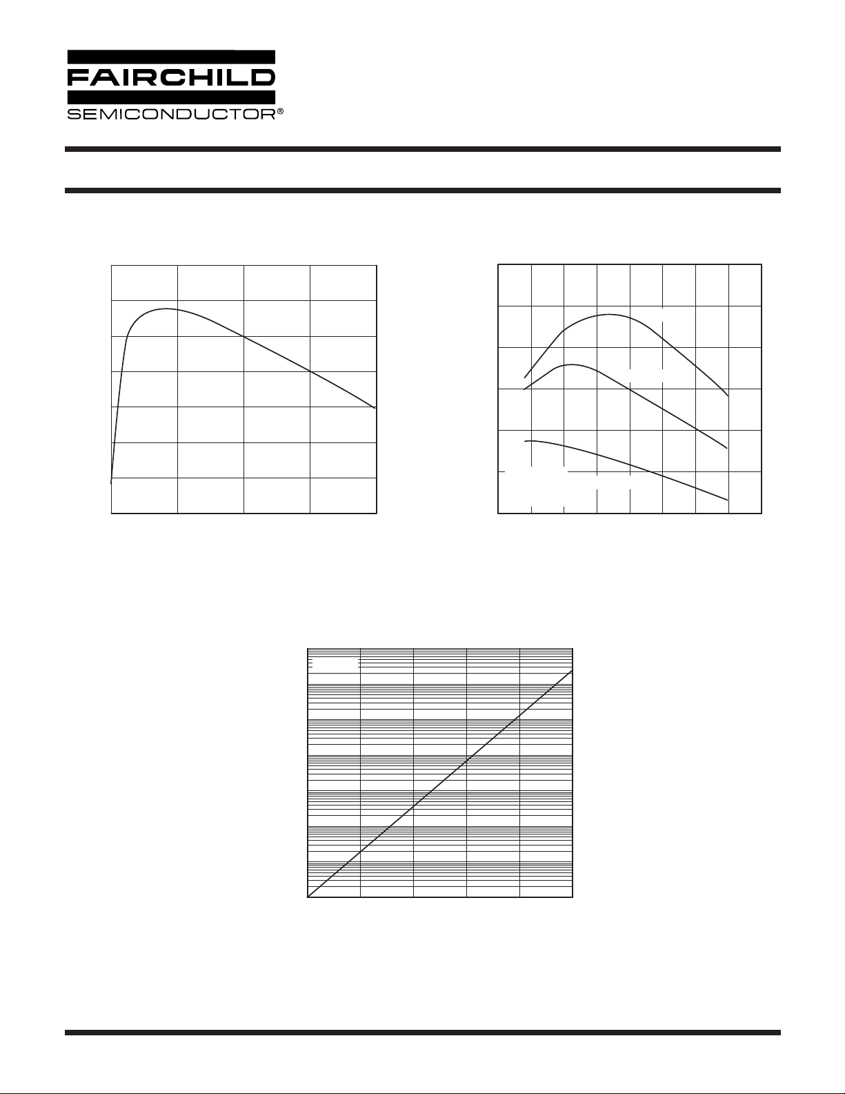
Normalized CTR vs. Forward Current
1.4
VCE = 5.0V
= 25˚C
T
A
1.2
1.0
0.8
0.6
NORMALIZED CTR
0.4
0.2
0.0
051015 20
IF - FORWARD CURRENT (mA)
10
10
1
0
Normalized to
I
F
VCE = 10 V
Normalized CTR vs. Ambient Temperature
1.6
= 10 mA
1.4
1.2
1.0
0.8
NORMALIZED CTR
0.6
Normalized to
= 10 mA
I
F
T
A
0.4
-75 -50 -25 0 25 50 75 100 125
Dark Current vs. Ambient Temperature
IF = 5 mA
IF = 10 mA
IF = 20 mA
= 25˚C
TA - AMBIENT TEMPERATURE (˚C)
- COLLECTOR-EMITTER DARK CURRENT (µA)
CEO
I
© 2003 Fairchild Semiconductor Corporation
-1
10
-2
10
-3
10
-4
10
-5
10
-6
10
0255075100 125
TA - AMBIENT TEMPERATURE (˚C)
Page 3 of 7
7/31/03
 Loading...