Fairchild Semiconductor MC79L08A Datasheet

©2002 Fairchild Semiconductor Corporation
www.fairchildsemi.com
Rev. 1.0.2
Features
• Output Current up to 100mA
• No External Components
• Internal Thermal Over Load Protection
• Internal Short Circuit Current Limiting
• Output Voltage Offered in ±5% Tolerance
• Output Voltage of -5V, -8V, -12V, -15V, -18V, -24V
Description
These regulators employ internal current limiting and
thermal shutdown, making them essentially indestructible.
TO-92
1
8-SOP
SOT-89
1
1.GND 2.Input 3.Output
1. Output 2.3.6.7. Input 5. GND 4.8. NC
1
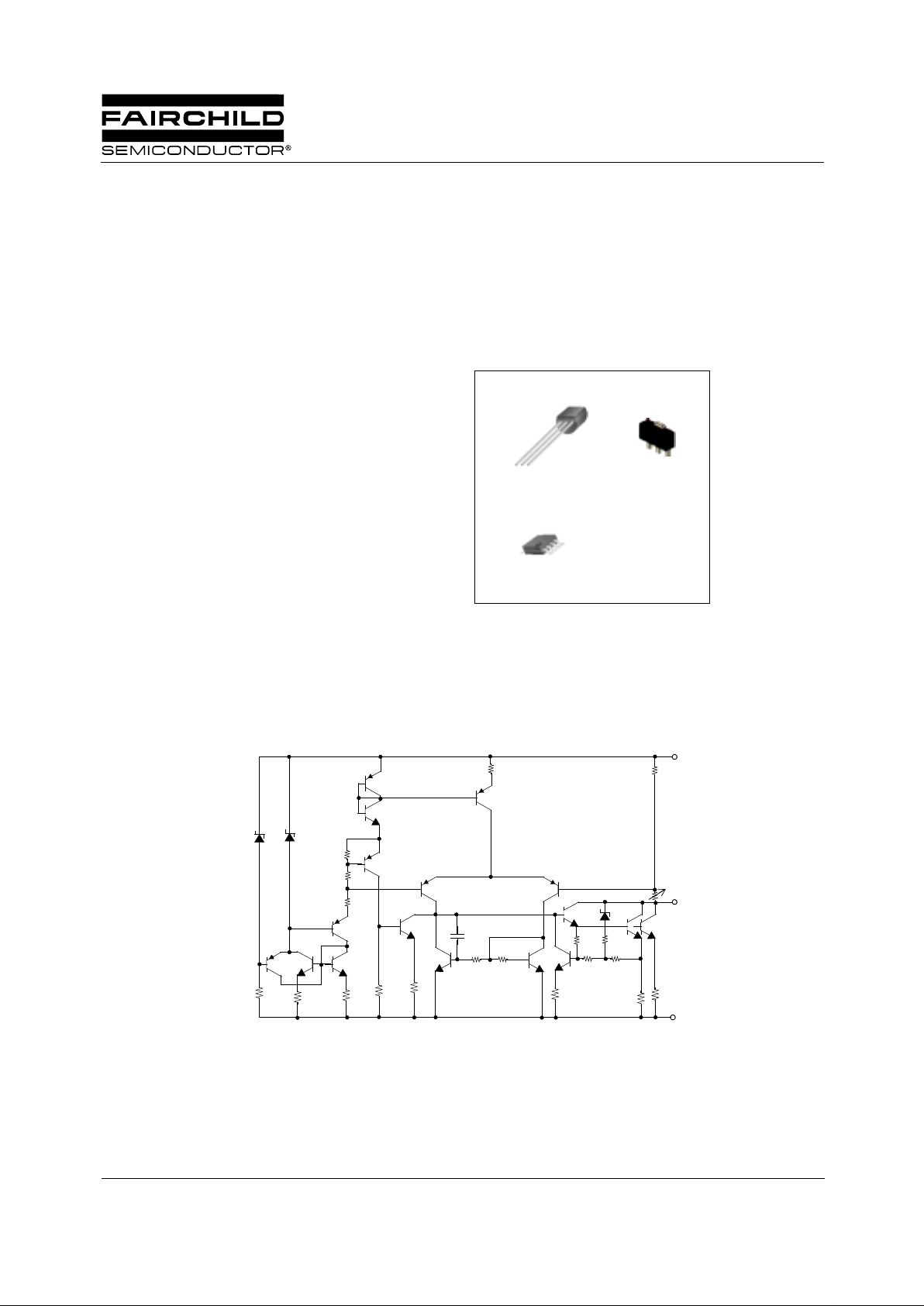
Internal Block Diagram
Q1
Q2
Q3
Q4
Q5
Q6
Q7
Q8
Q9
Q10
Q11
Q12
Q13Q14
Q15
Q16
Q17
R1
R2
R3
R4
R5
R6
R7
R15
R16
R17
R18
R26
R22
R24 R25
R29
R
R28
R23+R21
R27
D3
D2
D1
C1
GND
Output
Input
MC79LXXA/LM79LXXA
3-Terminal 0.1A Negative Voltage Regulator

MC79LXXA/LM79LXXA
2
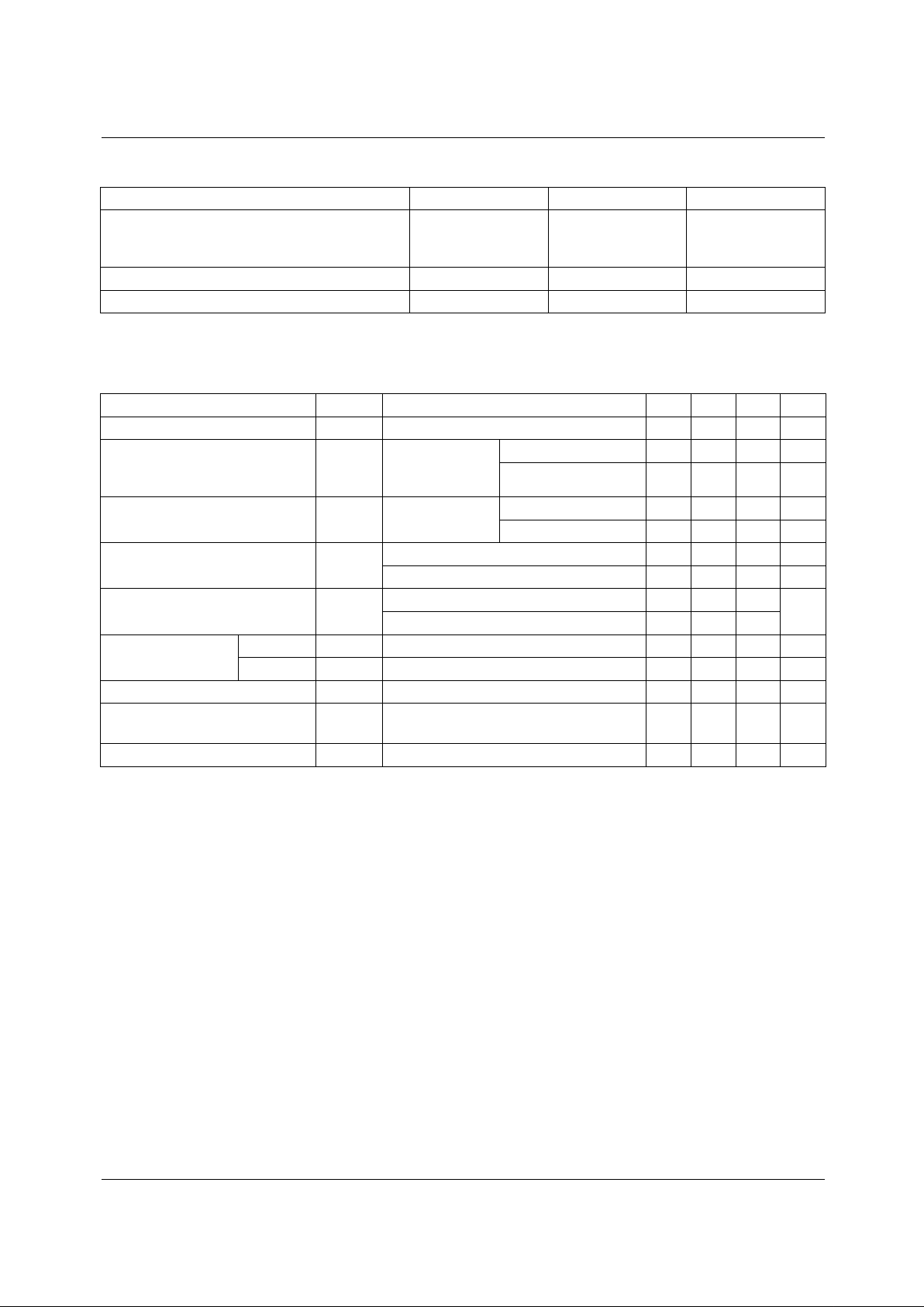
Absolute Maximum Ratings
Electrical Characteristics(MC79L05A/LM79L05A)
(VI = -10V, IO = 40mA, CI = 0.33µF, CO = 0.1µF, 0°C ≤T
J
≤ +125°C, unless otherwise specified)
Note:
1. Load and line regulation are specified at constant junction temperature. Change in V
O
due to heating effects must be taken
into account separately. Pulse testing with low duty is used.
Parameter Symbol Value Unit
Input Voltage (for V
o
= -5V to -8V)
(for V
O
= -12V to -18V)
(for V
O
= -24V)
V
I
-30
-35
-40
V
Operating Temperature Range T
OPR
0 ~ +125 °C
Storage Temperature Range T
STG
-65 ~ +150 °C
Parameter Symbol Conditions Min. Typ. Max. Unit
Output Voltage V
O
TJ = +25°C -4.8 -5.0 -5.2 V
Line Regulation (Note1) ∆V
O
TJ =+25°C
-7.0V ≥ V
I
≥ -20V - 15 150 mV
-8V ≥ VI ≥ -20V - - 100 mV
Load Regulation (Note1) ∆V
O
TJ =+25°C
1.0mA ≤ I
O
≤ 100mA - 20 60 mV
1.0mA ≤ I
O
≤ 40mA - 10 30 mV
Output Voltage V
O
-7.0V≥ V
I
≥ -20V, 1.0mA ≤ IO ≤ 40mA -4.75 - -5.25 V
V
I
= -10V, 1.0mA ≤ I
O
≤ 70mA -4.75 - -5.25 V
Quiescent Current I
Q
TJ =+25°C-2.05.5
mA
T
J
= +125°C--6.0
Quiescent Current
Change
With Line ∆I
Q
-8V ≥ V
I
≥ -20V - - 1.5 mA
With Load ∆I
Q
1.0mA ≤ I
O
≤ 40mA - - 0.1 mA
Output Noise Voltage V
N
TA = +25°C,10Hz ≤ f ≤ 100kHz - 30 - µV
Ripple Rejection RR
f = 120Hz, -8V ≥ V
I
≥ -18V
T
J
= +25°C
41 60 - dB
Dropout Voltage V
D
TJ = +25°C-1.7-V

MC79LXXA/LM79LXXA
3
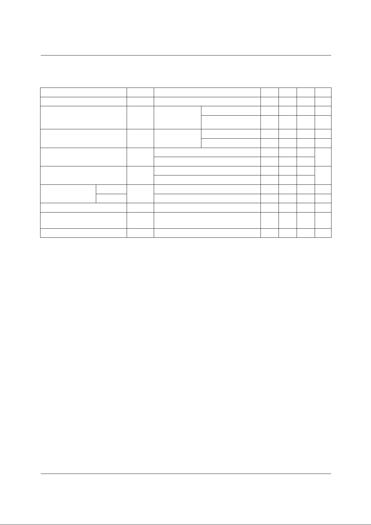
Electrical Characteristics (MC79L08A)
(Continued)
(VI = -14V, IO = 40mA, CI = 0.33µF, CO = 0.1µF, 0°C ≤T
J
≤ +125°C, unless otherwise specified)
Note:
1. Load an d lin e re gul ation ar e spec ifie d at con sta nt ju nct ion t empe rat ure. Chan ge i n V
O
due to heating effects must be taken
into account separately. Pulse testing with low duty is used.
Parameter Symbol Conditions Min. Typ. Max. Unit
Output Voltage V
O
TJ = +25°C -7.7 -8.0 -8.3 V
Line Regulation(Note1) ∆V
O
TJ = +25°C
-10.3V ≥ V
I
≥ -23V - - 175 mV
-12V ≥ VI ≥ -23V - - 125 mV
Load Regulation (Note1) ∆V
O
TJ = +25°C
1.0mA ≤ I
o
≤ 100mA - - 80 mV
1.0mA ≤ I
o
≤ 40mA - - 40 mV
Output Voltage V
O
-10.3V ≥ V
I
≥ -23V, 1.0mA ≤ Io ≤ 40mA -7.6 - -8.4
V
V
I
= -14V, 1.0mA ≤ I
o
≤ 70mA -7.6 - -8.4
Quiescent Current I
q
Tj = +25°C--6.0
mA
T
j
= +125°C--5.5
Quiescent Current
Change
With Line
∆I
Q
-11.7V ≥ V
I
≥ -23V - - 1.5 mA
With Load 1.0mA ≤ I
o
≤ 40mA - - 0.1 mA
Output Noise Voltage V
N
Tj = +25°C,10Hz ≤ f ≤ 100kHz - 50 - µV
Ripple Rejection RR
f = 120Hz, -11V ≥ V
I
≥ -21V
T
j
= +25°C
39 55 - dB
Dropout Voltage V
D
Tj = +25°C-1.7-V

MC79LXXA/LM79LXXA
4
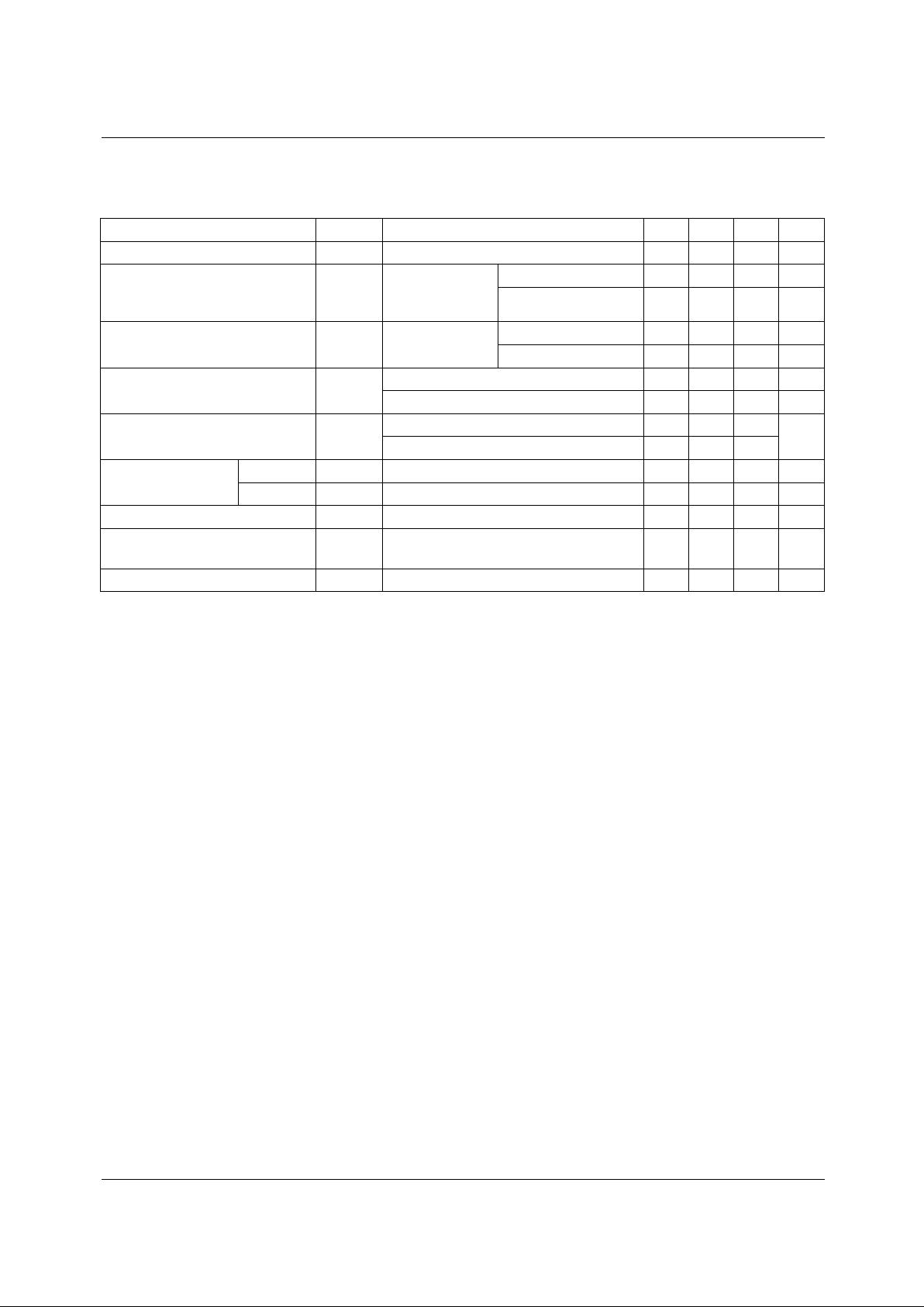
Electrical Characteristics(MC79L12A)
(Continued)
(VI = -19V, IO = 40mA, CI = 0.33µF, CO = 0.1µF, 0°C ≤T
J
≤ +125°C, unless otherwise specified)
Note:
1. Load and line regulation are specified at constant junction temperature. Change in V
O
due to heating effects must be taken
into account separately. Pulse testing with low duty is used.
Parameter Symbol Conditions Min. Typ. Max. Unit
Output Voltage V
O
TJ = +25°C -11.5 -12.0 -12.5 V
Line Regulation (Note1) ∆V
O
TJ = +25°C
-14.5V ≥ V
I
≥ -27V - - 250 mV
-16V ≥ VI ≥ -27V - - 200 mV
Load Regulation (Note1) ∆V
O
TJ = +25°C
1.0mA ≤ I
O
≤ 100mA - - 100 mV
1.0mA ≤ I
O
≤ 40mA - - 50 mV
Output Voltage V
O
-14.5V > V
I
> -27V, 1.0mA ≤ IO ≤ 40mA -11.4 - -12.6 V
V
I
= -19V, 1.0mA ≤ I
O
≤ 70mA -11.4 - -12.6 V
Quiescent Current I
Q
TJ = +25°C--6.0
mA
T
J
= +125°C--6.5
Quiescent Current
Change
With Line ∆I
Q
-16V ≥ V
I
≥ -27V - - 1.5 mA
With Load ∆I
Q
1.0mA ≤ I
O
≤ 40mA - - 0.1 mA
Output Noise Voltage V
N
TA = +25°C,10Hz ≤ f ≤ 100kHz - 80 - µV
Ripple Rejection RR
f = 120Hz, -15V≥ V
I
≥ -25V
T
J
= +25°C
37 42 - dB
Dropout Voltage V
D
TJ = +25°C-1.7-V
 Loading...