

Fairchild Semiconductor KSD1692 Datasheet
Feature
• High Dc Durrent Gain
• Low Collector Saturation Voltage
• Built-in a Damper Diode at E-C
• High Power Dissipation : P
= 1.3W (Ta=25°C)
C
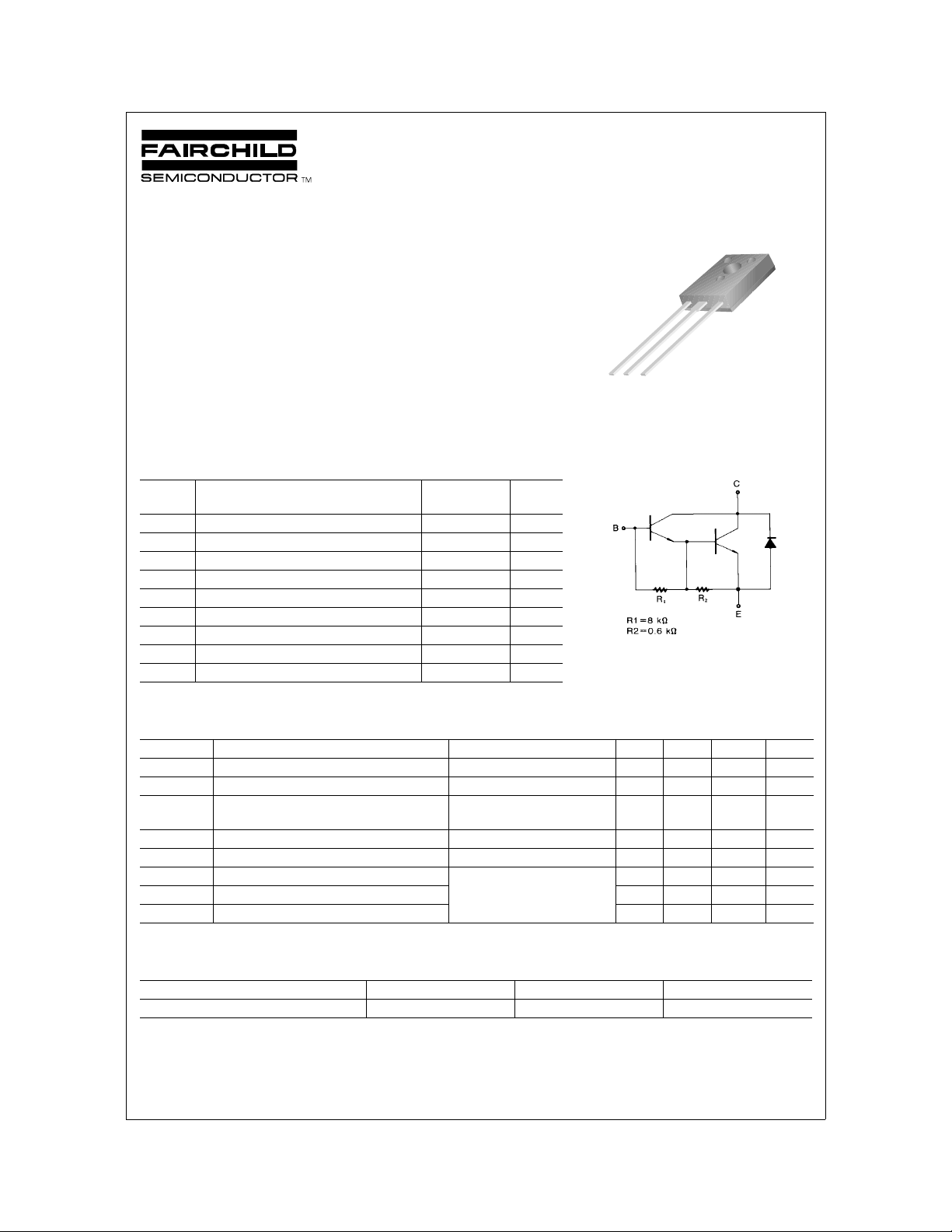
KSD1692
KSD1692
1
TO-126
1. Emitter 2.Collector 3.Base
NPN Silicon Darlington Transistor
Absolute Maximum Ratings
Sym-
bol
V
V
VEBO
IC
ICP
PC
P
T
T
* PW≤10ms, duty Cycle≤50%
Collector-Base Voltage 150 V
CBO
Collector-Emitter Voltage 100 V
CEO
Emitter-Base Voltage 8 V
Collector Current (DC) 3 A
*Collector Current (Pulse) 5 A
Collector Dissipation (Ta=25°C) 1.3 A
Collector Dissipation (TC=25°C) 15 W
C
Junction Temperature 150 W
J
Storage Temperature - 55 ~ 150 °C
STG
Parameter Value Units
Electrical Characteristics
Symbol Parameter Test Condition Min. Typ. Max. Units
I
CBO
IEBO
hFE1
h
FE2
(sat) *Collector-Emitter Saturation Voltage IC = 1.5A, IB = 1.5mA 0.9 1.2 V
V
CE
(sat) *Base-Emitter Saturation Voltage IC = 1.5A, IB = 1.5mA 1.5 2 V
V
BE
t
ON
t
STG
t
F
* Pulse test: PW≤350µs, duty Cycle≤2% Pulsed
Collector Cut-off Current V
Emitter Cut-off Current V
*DC Current Gain V
Turn ON Time V
Storage Time 2 µs
Fall Time 1 µs
TC=25°C unless otherwise noted
TC=25°C unless otherwise noted
= 100V, IE = 0 10 µA
CB
= 5V, IC = 0 2 mA
EB
= 2V, IC = 1.5A
CE
V
= 2V, IC = 3A
CE
= 40V, IC = 1.5A
CC
= - IB2 = 1.5mA
I
B1
= 27Ω
R
L
2K
1K
0.5 µs
20K
hFE Classificntion
Classification O Y G
h
FE1
©2000 Fairchild Semiconductor International Rev. A, February 2000
2000 ~ 5000 4000 ~ 12000 6000 ~ 20000
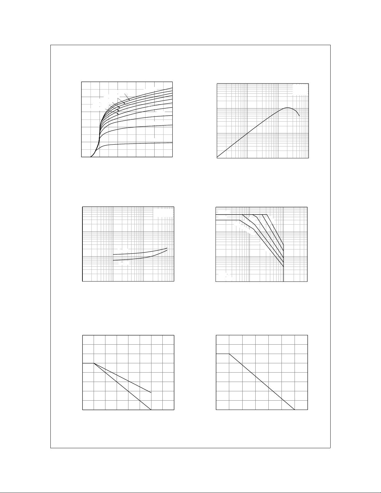
Typical Characteristics
KSD1692
IB = 450uA
= 500uA
I
B
= 200uA
I
B
= 150uA
I
B
IB = 100uA
IB = 50uA
5
IB = 350uA
IB = 300uA
IB = 250uA
IB = 400uA
4
3
2
1
Ic[A], COLLECTOR CURRENT
0
012345
VCE[V], COLLECTOR-EMITTER VOLTAGE
Figure 1. Static Characteristic Figure 2. DC current Gain
100
10
1
(sat)[V], SATURATION VOLTAGE
CE
(sat), V
BE
V
0.1
IC[A], COLLECTOR CURRENT
Ic = 1000 I
Pulsed
VBE(sat)
VCE(sat)
0.1 1 10
100000
10000
1000
, DC CURRENT GAIN
FE
h
100
0.01 0.1 1 10
VCE = 2V
Pulsed
IC[A], COLLECTOR CURRENT
200ms
10ms
1ms
s/b Limited
300us
100us
B
10
Ic(Pulse)
Ic(DC)
Dissipation Limited
1
0.1
[A], COLLECTOR CURRENT
C
I
Tc=25oC
Single Pulse
0.01
1 10 100 500
VCE[V], COLLECTOR-EMITTER VOLTAGE
Figure 3. Collector-Emitter Saturation Voltage
Figure 4. Forward Bias Safe Operating Areas
Base-Emitter Saturation Voltage
[%], Ic DERATING
T
d
160
140
120
100
80
60
40
20
0
25 50 75 100 125 150 175 200
s/b LIMITED
DISSIPATION LIMITED
TC[oC], CASE TEMPERATURE
20
15
10
5
[W], POWER DISSIPATION
C
P
0
0 25 50 75 100 125 150 175
TC[oC], CASE TEMPERATURE
Figure 5. Derating Curve of Safe Operating Areas Figure 6. Power Derating
©2000 Fairchild Semiconductor International
Rev. A, February 2000
 Loading...