

High Voltage Switching
Low Power Switching Regulator
DC-DC Converter
• High Breakdown Voltage
• Low Collector Saturation Voltage
• High Speed Switching
PNP Silicon Transistor
KSA1156
1
TO-126
1. Emitter 2.Collector 3.Base
KSA1156
Absolute Maximum Ratings
TC=25°C unless otherwise noted
Symbol Parameter Ratings Units
V
CBO
V
CEO
V
EBO
I
B
I
C
I
CP
P
C
P
C
T
J
T
STG
Electrical Characteristics
Collector-Base Voltage - 400 V
Collector-Emitter Voltage - 400 V
Emitter-Base Voltage - 7 V
Base Current - 0.25 A
Collector Current (DC) - 0.5 A
Collector Current (Pulse) - 1 A
Collector Dissipation (Ta=25°C) 1 W
Collector Dissipation (TC=25°C) 10 W
Junction Temperature 150 °C
Storage Temperature - 55 ~ 150 °C
TC=25°C unless otherwise noted
Symbol Parameter Test Condition Min. Max. Units
V
(sus) Collector-Emitter Sustaining Voltage IC = - 100mA, IB = - 10mA
CEO
- 400 V
L = - 20mH
(sus) Collector-Emitter Sustaining Voltage
V
CEX
I
CBO
I
EBO
I
CEX1
I
CEX2
h
FE
(sat) Collector-Emitter Saturation Voltage IC = - 100mA, IB = - 10mA - 1 V
V
CE
(sat) Base-Emitter Saturation Voltage IC = - 100mA, IB = - 10mA - 1.2 V
V
BE
t
ON
t
STG
t
F
Collector Cut-off Current VCB = - 400V, IE = 0 - 100 µA
Emitter Cut-off Current VEB = - 5V, IC = 0 - 10 µA
Collector Cut-off Current VCE = - 400V, VBE(off) = 1.5V - 100 µA
Collector Cut-off Current VCE = - 400V, VBE(off) = 1.5V
DC Current Gain VCE = - 5V, IC = - 100mA 30 200
Turn On Time VCC = - 150V, IC = - 100mA
Storage Time 4 µs
Fall Time 1 µs
IC = - 200mA, IB1 = - IB2 = - 20mA
(off)= 5V, L = 10mH
V
BE
= 125°C
T
C
I
= - 10mA , IB2 = 20mA
B1
= 1.5KΩ
R
L
- 400 V
- 1 mA
1 µs
hFE Classification
Classification N R O Y
h
FE
©2000 Fairchild Semiconductor International Rev. A, February 2000
30 ~ 60 40 ~ 80 60 ~ 120 100 ~ 200
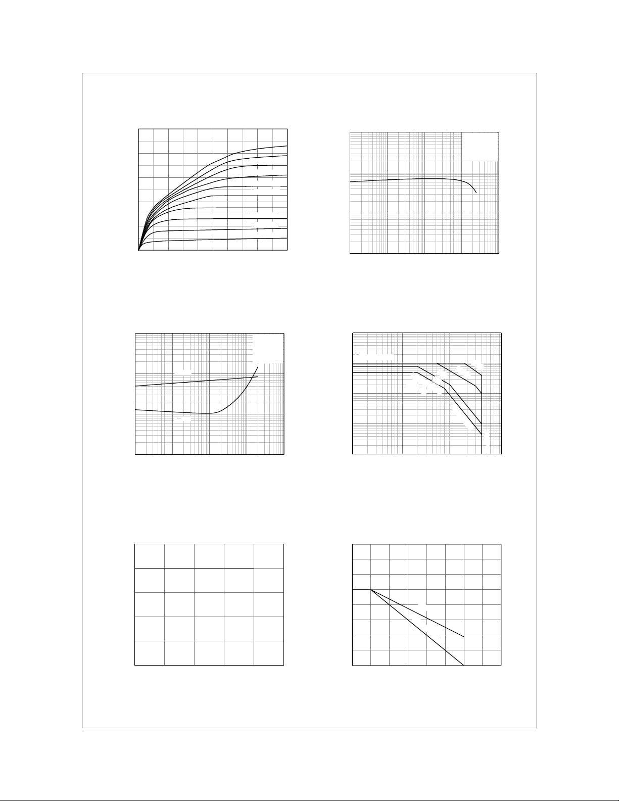
Typical Characteristics
KSA1156
-0.5
-0.4
-0.3
-0.2
[A], COLLECTOR CURRENT
-0.1
C
I
-0.0
-0 -2 -4 -6 -8 -10
VCE[V], CO LLEC TOR-E MITTER VOLTAGE
Figure 1. Static Characteristic Figure 2. DC current Gain
-10
-1
-0.1
(sat)[V], SATURATION VOLTAGE
CE
(sat), V
BE
V
-0.01
-0.1 -1 -10 -100 -1000
VBE(sat)
VCE(sat)
IC[mA], COLLECTOR CURRENT
IB = -200mA
IB = -180mA
IB = -160mA
IB = -140mA
IB = -120mA
IB = -100mA
= -80mA
I
B
IB = -60mA
IB = -40mA
IB = -20mA
IC = 10 I
1000
VCE = -5V
Pulse Test
100
10
, DC CURRENT GAIN
FE
h
1
-0.1 -1 -10 -100 -1000
IC[A], COLLECTOR CURRENT
DISSIPATION
LIMITED
10
㎲
100
1ms
DC
㎲
S/b LIMITED
MAX.
CEO
V
-10
B
IC MAX. (Pulse)
-1
-0.1
-0.01
[A], COLLECTOR CURRENT
C
I
-1E-3
-1 -10 -100 -1000
VCE[V], COLLECTOR-EMITT E R VOL TA G E
Figure 3. Collector-Emitter Saturation Voltage
Base-Emitter Saturation Voltage
-250
-200
-150
-100
-50
(mA), COLLECTOR CURRENT
C
I
-0
-0 -100 -200 -300 -400 -500
VCE(v), COLLECTOR EMITTER VOLTAGE
Figure 5. Reverse Bias Safe Operating Area Figure 6. Derating Curve of Safe Operating Areas
©2000 Fairchild Semiconductor International
Figure 4. Safe Operating Area
160
140
120
100
80
DERATING
c
60
dT(%),I
40
20
0
0 50 100 150 200
TC[oC], CASE TEMPERATURE
S/b Limited
Dissipation Limited
Rev. A, February 2000
 Loading...