

Fairchild Semiconductor KF353 Datasheet
KF353
Dual Operational Amplifier (JFET)
www.fairchildsemi.com
Features
• Internally trimmed offset voltage: 10mV
• Low input bias current: 50pA
• Wide gain bandwidth: 4MHz
• High slew rate: 13V/µs
• High Input impedance: 10
12
Ω
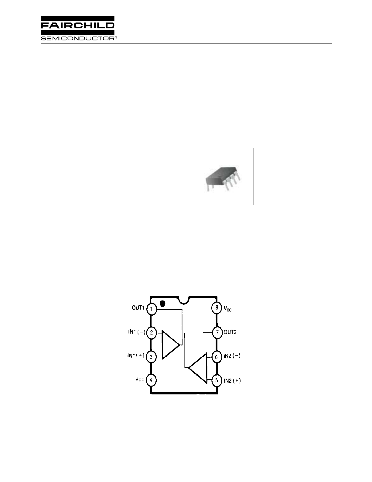
Internal Block Diagram
Description
The KF353 is a JFET input operational amplifier with an
internally compensated input offset voltage. The JFET input
device provides wi de bandwid th, low input bias curre nts and
offset currents.
8-DIP
1
©2001 Fairchild Semiconductor Corporation
Rev. 1.0.1
KF353
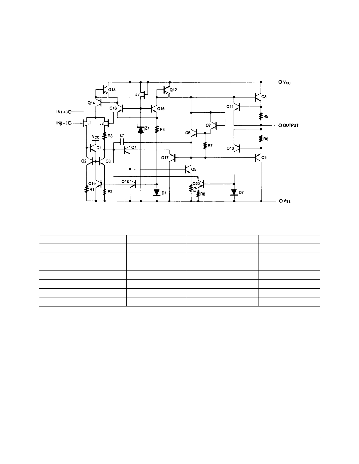
Schematic Diagram
(One Section Only)
Absolute Maximum Ratings
Parameter Symbol Value Unit
Power Supply Voltage V
Differential Input Voltage V
Input Voltage Range V
CC
I(DIFF)
I
Output Short Circuit Duration - Continuous Power Dissipation P
Operating Temperature Range T
Storage Temperature Range T
D
OPR
STG
±18 V
30 V
±15 V
500 mW
0 ~ +70 °C
-65 ~ +150 °C
2
 Loading...