Fairchild Semiconductor KF351 Datasheet

KF351
Single Operational Amplifier (JFET)
www.fairchildsemi.com
Features
• Internally trimmed offset voltage: 10mV
• Low input bias current : 50pA
• Wide gain bandwidth : 4MHz
• High slew rate : 13V/µs
• High input impedance : 10
12
Ω
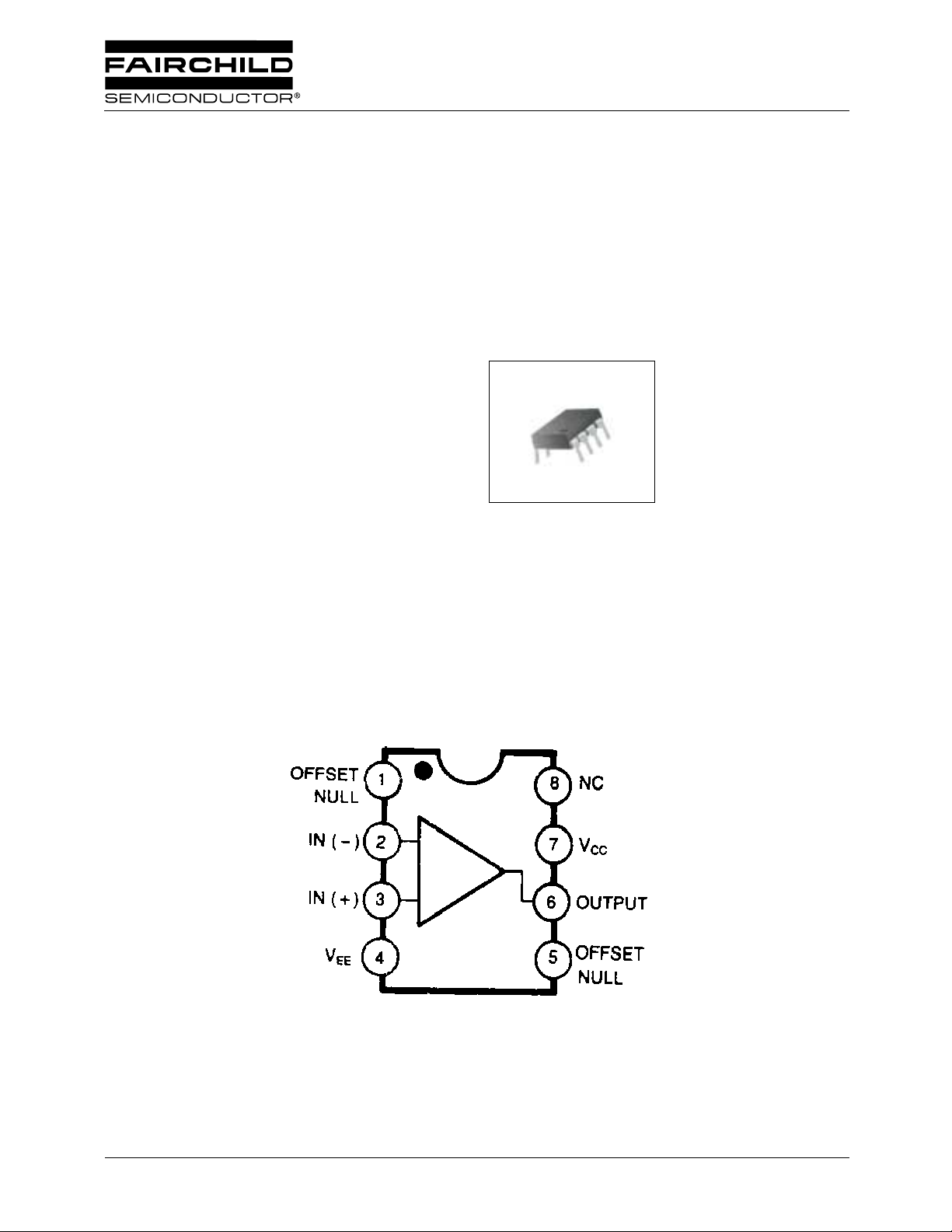
Internal Block Diagram
Description
The KF351 is JFET input operational amplifier with an
internally compensated input offset voltage. The JFET input
device provides wide bandwidth, low input bias currents and
offset currents.
8-DIP
1
©2001 Fairchild Semiconductor Corporation
Rev. 1.0.0

KF351
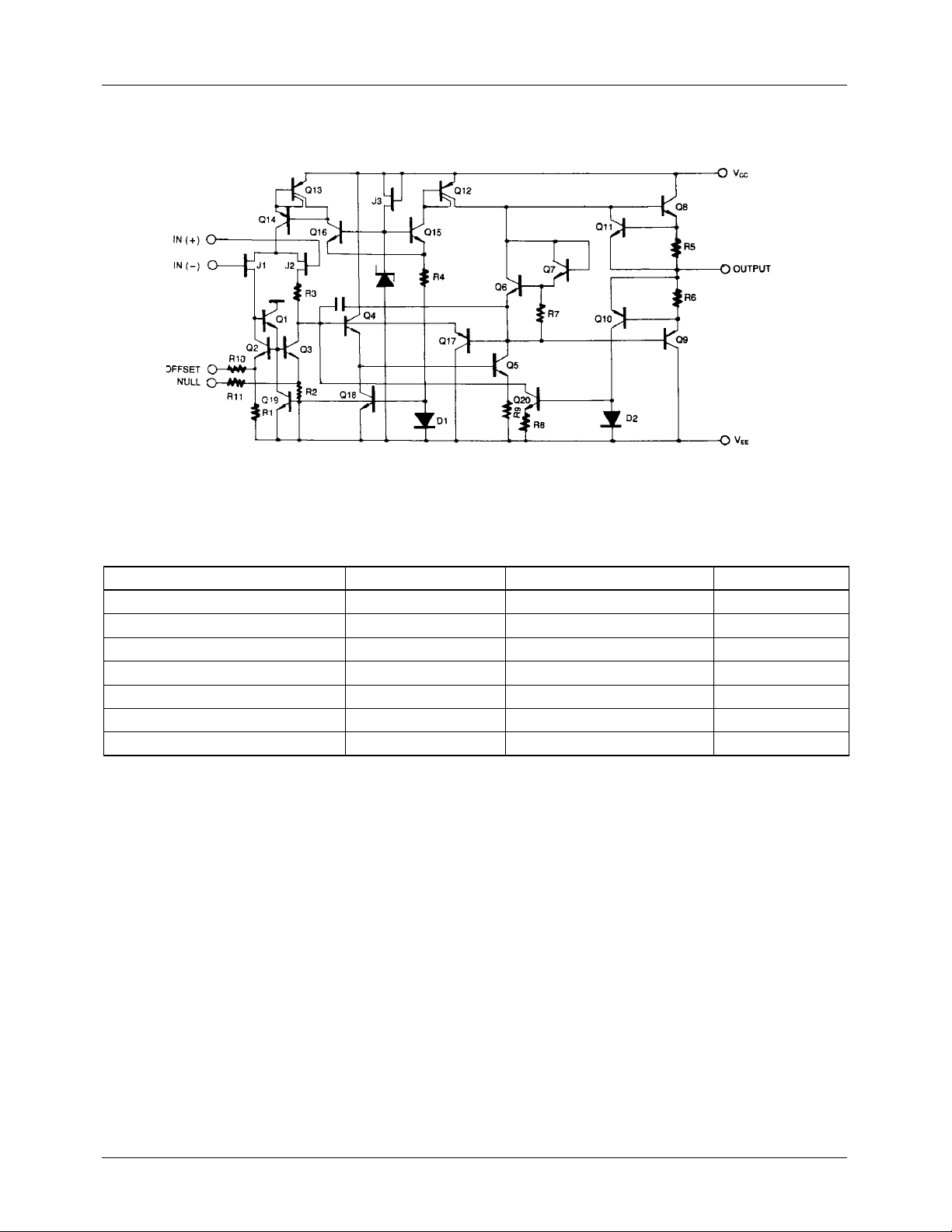
Schematic Diagram
Absolute Maximum Ratings
Parameter Symbol Value Unit
Supply Voltage V
Differential Input Voltage V
Input Voltage Range V
CC
I(DIFF)
I
Output Short Circuit Duration - Continuous Power Dissipation P
Operating Temperature T
Storage Temperature Range T
D
OPR
STG
±18 V
30 V
±15 V
500 mW
0 ~ +70 °C
-65 ~ +150 °C
2
 Loading...