Fairchild Semiconductor KA7577 Datasheet

KA7577
SMPS Controller
www.fairchildsemi.com
Features
• Low Stand-By Current
• Pulse by Pulse Current Limiting
• Over Voltage Protection
• Over Current Protection
• Integrated Th e rm al Shutdown Circuit
• Output Driver Current of ± 2A
• Totem pole Output
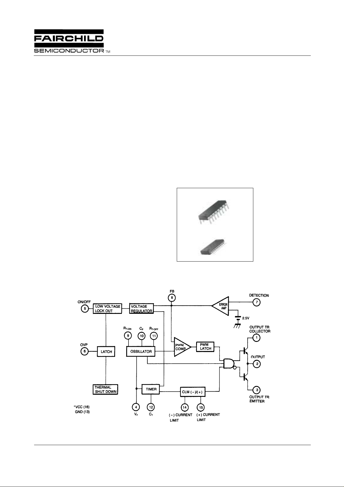
Internal Block Diagram
Description
KA7577 is fixed frequency PWM controller and specially
designed for SMPS to get regulated DC voltage from AC
power supply. This integrated circuit has so fast rise and fall
output pulse that it can directly drive power transistor as well
as power MOSFET. This device features high speed and
high sensitive current limiting. Protection circuitry include
current limiting function against short and over current at
secondary side, owing to the integrated timertype-protection
circuit.
16-DIP
1
20-SOP
1
©2000 Fairchild Semiconductor International
Rev. 5.0

KA7577
Absolute Maximum Ratings
Parameter Symbol Value Unit
Supply Voltage V
Collector Supply Voltage V
Output DC Current I
Output Peak Voltage I
V
Terminal Voltage V
F
V
ON/OFF
Terminal Voltage V
Current Limiting (-) Terminal Voltage V
Current Limiting (+) Terminal Voltage V
Over Voltage Protection Terminal Voltage V
Detection Terminal Voltage (Note 1) V
Detection Terminal Sink Current (Note 1) I
Feedback Terminal Voltage V
Timer ON Terminal Source Current I
Timer OFF Terminal Source Current I
Power Dissipation P
hermal Derating Factor K
Operating Temperature Range T
Storage Temperature Range T
Junction Temperature T
Note:
1. This terminal has the constant voltage characteristics of 6-8V, when current is supplied from out side.
The maximum allowable voltage is 6V when the constant voltage is applied to this terminal.
And maximum allowable current is 5mA, it is recommended to use current limiting resistor.
CC
C
O(DC)
OPK
(VF)
(ON/OFF)
(CLM - )
(CLM +)
(OVP)
(DET)
SINK(DET)
(FB)
SOURCE(T-ON)
SOURCE(T-OFF)
D
TD
OPR
STG
J
31 V
31 V
± 0.5 A
± 2A
31 V
31 V
- 4 ~+4 V
- 0.3 ~+4 V
31 V
6V
5mA
0 - 10 V
-1 mA
-1 mA
1.5 W
12 mW/°C
- 25 ~ +85 °C
- 40 ~ +125 °C
150 °C
2

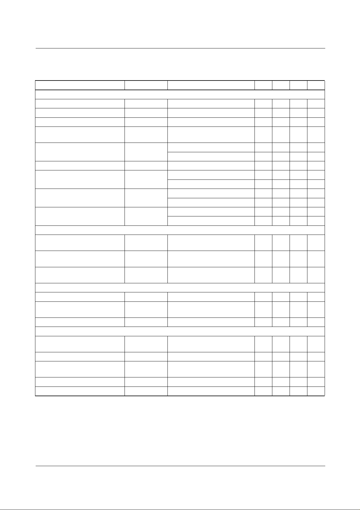
Electrical Characteristics
(VCC = 18V, TA = 25°C, unless otherwise specified)
Parameter Symbol Conditions Min. Typ. Max. Unit
POWER SUPPLY VOLTAGE AND CURRENT SECTION
Power Supply Voltage V
Operation Start-Up Voltage V
Operation Stop Voltage V
Difference Voltage Between
Operation Start and Stop
Stand-By Current I
Operating Supply Current I
Supply Current at Non-Operating I
Supply Current at Timer NonOperating
Supply Current at OVP Operating I
ON/OFF SECTION
ON/OFF Terminal High
Threshold Voltage
ON/OFF Terminal Low Threshold
Voltage
ON/OFF Terminal Hysteresis
Voltage
DETECTION SECTION
Detection Voltage V
Input Current of Detection
Voltage
Voltage Gain of Detection Amp G
FEEDBACK SECTION
Current at Min Duty Cycle I
CC
CC(START)
CC(STOP)
∆V
CC
SB
CC(OPR)
CC(OFF)
I
CC(CT)
CC(OVP)
V
THH(ON/OFF)
V
THL(ON/OFF)
V
HYS(ON/OFF)
(DET)
I
I(DET)
V(DET)
FB(MIND)
TA = 25°C, VCC = 14.5V 50 80 140 µA
T
V
VCC = 25V 0.95 1.31 1.9 mA
V
VCC = 25V 0.95 1.35 2.0 mA
V
V
V
V
---30V
- 15.2 16.2 17.2 V
- 9.0 9.9 10.9 V
- 5.0 6.3 7.6 V
= -30 to +85°C, VCC = 14.5V 40 80 160 µA
A
= 30V 13 15 21 mA
CC
= 14V 50 80 120 µA
CC
= 14V - 140 220 µA
CC
= 25V 1.0 2.0 3.0 mA
CC
= 9.5V 125 190 290 µA
CC
- 2.1 2.6 3.1 V
- 1.9 2.4 2.9 V
- 0.1 0.2 0.3 V
- 2.4 2.5 2.6 V
= 2.5V - 1.0 3.0 µA
(DET)
-4055-dB
- - 2.1 -1.54 -1.0 mA
KA7577
Current at Max Duty Cycle I
Current Difference Between Max
and Zero Duty Cycle
FB(MAXD)
∆I
FB Terminal Voltage V(
FB Terminal Resistance R
(FB)
FB)
(FB)
- - 0.9 - 0.55 - 0.4 mA
- -1.35 - 0.99 - 0.7 mA
I
= - 0.95mA 4.9 5.9 7.1 V
SINK
V
= 2.5V - 500 - W
(DET)
3
 Loading...