


November 2,1999
AN4003
PC POWER SUPPLY DESIGN WITH KA3511
Sang-Tae Im
1. GENERAL DESCRIPTION
The KA3511 is a fixed-frequency improved-performance pulse-width modulation control circuit with
complete housekeep ing circuitry for use in the s econdary side of SMPS (Swit ched mode power
supply). It cont ains variou s functions, which are p recision vol tage referenc e, over vol tage protection, under voltage protection, remote on/off control, power good signal generator and etc.
OVP (Over voltage protection) section
It has OVP functio ns for +3.3V,+5V,+12V and PT outputs. The circu it is made u p of a com parator
with four detecting inpu ts a nd wi thou t hysteresis voltage. Especi al ly, PT (Pin16) is prepared for an
extra OVP input or another protection signal.
UVP (Under voltage protection) section
It also has UVP functions for +3.3V , +5V, +12V outputs. The block is made up of a comparator with
three detecting inputs and without hysteresis voltage.
Remote on/off section
Remote on/off section is used to control SMPS externally. If a high signal is supplied to the remote
on/off input, PWM signal becomes a high state and all secondary outputs are grounded. The
remote on/off signal is transferred with some on- delay and off-delay time of 8ms, 24ms respectively.
Precision reference section
The reference voltage trimmed to ±2% (4.9V<Vref<5.1V)
PG (Power good signal generator) section
Power good signal generator is to monitor the voltage level of power supply for safe operation of a
microprocessor.
KA3511 requires few external components to accomplish a complete housekeeping circuits for
SMPS. The KA3511 is available in a 22-pin dual in-line package.
Rev C, November 1999
1
ORDERING INFORMATION
Device Package Operating Temperature
KA3511 22 DIP -25°C ~ 85°C
FEATURES
• Complete PWM control and hou se ke epi ng circ uitr y
• Few external components
• Precision voltage reference trimmed to 2%
• Dual output for push-pull opera tio n
• Each output TR for 200mA sink current
• Variable duty cycle by dead time control
• Soft start capability by using dead time control
• Double pulse suppression logic
• Over voltage protection for 3.3V / 5V / 12V
• Under voltage protection for 3.3V / 5V / 12V
• One more external input for various protection (PT)
• Remote on/off control function (PS-ON)
• Latch function controlled by remote and protection input
• Power good signal generator with hysteresis
• 22-Pin dual in-line package
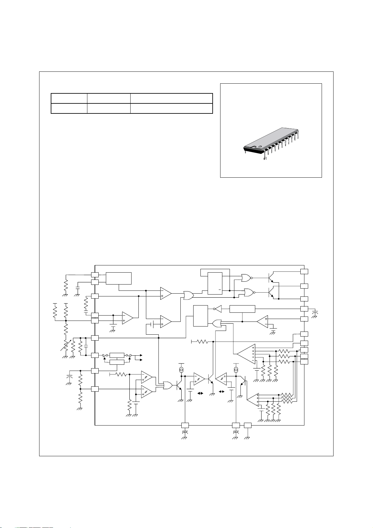
2. BLOCK DIAGRAM
22-DIP-400
V5 V12
E/A(-)
E/A(+)
DEAD TIME
CONTROL
R
T
C
T
COMP
19
12 VREF
VREF
V
CC
DET
C1
7
OSCILLATOR
8
2
3
4
1
9
5V
Start Up
1.25V
INTERNAL
BIAS
1.25V
0.1V
COMP1
COMP2
PWM
CONTROL
DEAD TIME
CONTROLLER
Ichag
T
VREF
PG
5V
2.2uF
R
Q
S
PG
GENERATOR
COMP3
1.8V 0.6V
DQ
CK
Q
1.8V 0.6V
CONTROLLER
T
UVP
2.2uF
DELAY
VREF
17 1810
OVP
COMP
UVP
COMP
REMOTE ON/OFF
1.4V
1.25V
1.25V
GND
22
20
21
5
6
11
16
15
14
13
T
REM
(PS-ON)
C2
E
REM
PG
PT
V12
V5
V3.3
Rev C, November 1999
2
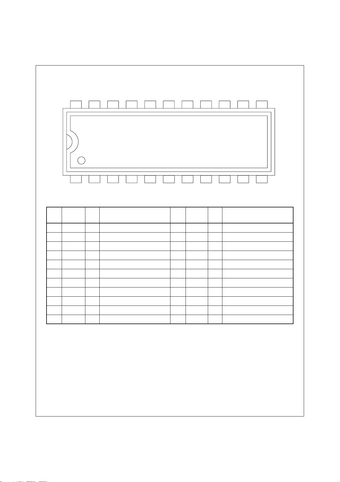
3. PIN DESCRIPTION
Vref
#12
#22
V3.3
V5V12PTTUVPGNDDTCC2EC1
KA3511
#1 #11
V
COMP E/A(-) EA(+) TREM REM RT CT DET TPG PG
CC
Pin
No. Name I/O Function
1 V
I Supply voltage 12 Vref O Precision reference VTG
CC
2 COMP O E/A output 13 V3.3 I OVP, UVP input for 3.3V
3 E/A(-) I E/A (-) input 14 V5 I OVP, UVP input for 5V
4 E/A(+) I E/A (+) input 15 V12 I OVP, UVP input for 12V
5 TREM – Remote on/off delay 16 PT I Extra protection input
6 REM I Remote on/off input 17 T
7 RT – Oscillation freq. setting R 18 GND – Signal ground
8 CT – Oscillation freq. setting C 19 DTC I Deadtime control input
9 DET I Detect input 20 C2 O Output 2
10 T
PG
– PG delay 21 E – Power ground
11 PG O Power good signal output 22 C1 O Output 1
Pin
No. Name I/O Function
– UVP delay
UVP
Rev C, November 1999
3

Pin
No. Name Function
1 V
Supply voltage. Operating range is 14V~30V. VCC =20V, Ta=25°C at test.
CC
2 COMP Error amplifier output. It is connected to non-inverting input of pulse width
modulator comparator.
3 E/A(-) Error amplifier inverting input. Its reference voltage is always 1.25V.
4 E/A(+) Error amplifier non-inverting input feedback voltage.This pin may be used to
sense power supply output volt age .
5 TREM Remote on/off delay. Ton/Toff=8ms/24ms (Typ.) with C=0.1µF. Its high/low
threshold voltage is 1.8V/0.6V.
6 REM Remote on/off input. It is TTL operation and its threshold voltage is 1.4V. Voltage
at this pin can reach normal 4.6V, with absolutely maximum voltage, 5.25V. If
REM = “Low”, PWM = “Low”. That means the main SMPS is operational. When
REM = “High”, then PWM = “High” and the main SMPS is turned-off.
7 RT Oscillation frequency setting R. (Test Condition R
8 CT Oscillation frequency setting C. (Test Condition C
=10kΩ)
T
=0.01µF)
T
9 DET Under-voltage detect pin. Its threshold voltage is 1.25V Typ.
10 T
PG delay. Td=250ms (Typ) with CPG=2.2µF. The high/low threshold voltage are
PG
1.8V/0.6V and the voltage of Pin10 is clamped at 2.9V for noise margin.
11 PG Power good output signal. PG = “High” means that the power is “Good” for
operation and PG = “Low” means “Power fail”.
12 Vref Precision voltage reference trimmed to 2%. (Typical Value = 5.03V)
13 V3.3 Over voltage protection for output 3.3V. (Typical Value = 4.1V)
14 V5 Over voltage protection for output 5V. (Typical Value = 6.2V)
15 V12 Over voltage protection for output 12V. (Typical Value = 14.2V)
16 PT This is prepared for an extra OVP input or another protection signal. (Typical
Value = 1.25V)
17 T
Timing pin for under voltage protection blank-out time. Its threshold voltage is
UVP
1.8V and clamped at 2.9V after full charging. Target of delay time is 250ms and
it is realized through external (C=2.2µF).
18 GND Signal ground.
19 DTC Deadtime control input. The dead-time control comparator has an effective
120mV input offset which limits the minimum output dead time. Dead time may
be imposed on the output by setting the dead time control input to a fixed
voltage, ranging between 0V to 3.3V.
20 C2 Output drive pin for push-pull operation.
21 E Power ground.
22 C1 Output drive pin for push-pull operation.
Rev C, November 1999
4
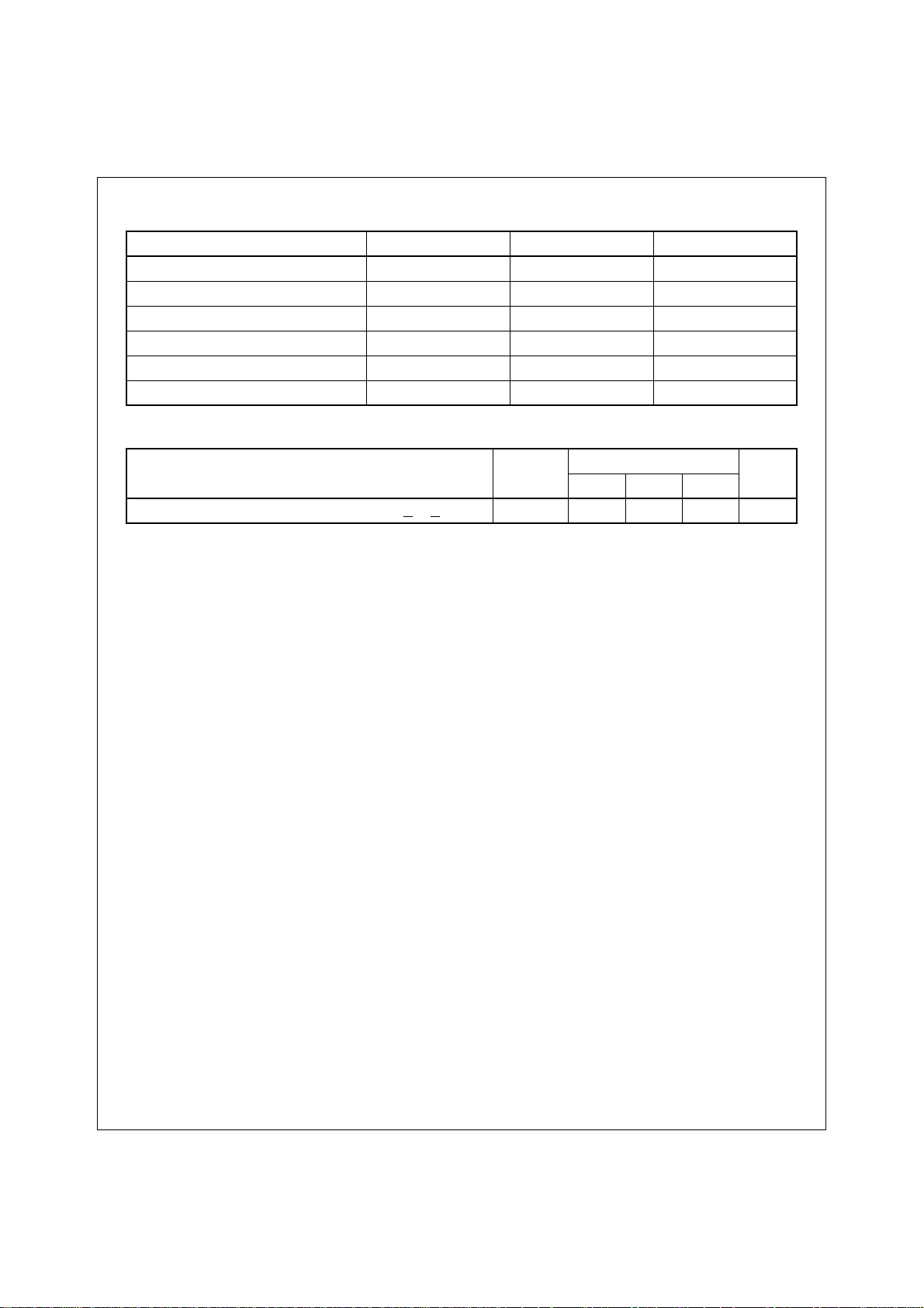
4. ABSOLUTE MAXIMUM RATINGS
Characteristic Symbol Value Unit
Supply voltage V
Collector output voltage V
Collector output current I
C1
C1
CC
, V
, I
Power dissipation P
Operating temperature T
Storage temperature T
OPR
STG
TEMPERATURE CHARACTERISTICS
Characteristic Symbol
Temperature coefficient of Vref (-25 °C<
Ta<85°C)∆Vref/∆T – 0.01 – %/°C
D
C2
C2
40 V
40 V
200 mA
1 W
-25 to 85 °C
-65 to 150 °C
Value
Unit Min. Typ. Max.
Rev C, November 1999
5
5. ELECTRICAL CHARACTERISTICS
(VCC =20V, TA =25°C)
Value
Characteristic Symbol Test Condition
REFERENCE SECTION
Reference output voltage Vref Iref=1mA 4.9 5 5.1 V
Line regulation
Load regulation
Temperature coefficient of Vref
Short-circuit output current I
∆
Vref.
LINE
∆
Vref.
(1)
∆Vref/∆T -25°C<Ta<85°C – 0.01 – %/°C
LOAD
SC
14V<VCC<30V – 2.0 25 mV
1mA<Iref<10mA – 1.0 15 mV
Vref=0 15 35 75 mA
OSCILLATOR SECTION
Oscillation frequency fosc C
Frequency change with
temperature
(1)
fosc/T CT=0.01µF, RT=12k – 2 – %
=0.01µF, RT=12k – 10 – kHz
T
DEAD TIME CONTROL SECTION
Input bias current I
Maximum duty voltage DC
Input threshold voltage V
TH(DT)
B(DT)
Pin19 (DTC)=0V 45 48 50 %
MAX
Zero Duty Cycle – 3.0 3.3 V
– -2.0 -10 µA
Max. Duty Cycle 0 – –
ERROR AMP SECTION
Inverting reference voltage Vref(EA) 1.20 1.25 1.30 %
Input bias current I
Open-loop voltage gain
Unit-gain bandwidth
(1)
(1)
Output sink current I
Output source curren t I
B(EA)
V
GVO 0.5V<V
BW – 650 – kHz
SINK
SOURCE
V
V
=2.5V – -0.1 -1.0 µA
COMP
<3.5V 70 95 – dB
COMP
=0.7V 0.3 0.9 – mA
COMP
=3.5V -2.0 -4.0 – mA
COMP
PWM COMPARATOR SECTION
Input threshold voltage V
TH(PWM)
Zero Duty Cycle – 4 4.5 V
OUTPUT SECTION
Output saturation voltag e V
CE(SAT)
Collector off-state current I
Rising time T
Falling time T
IC=200mA – 1.1 1.3 V
C(off)
R
F
VCC=VC=30V, VE=0V – 2 100 µA
– 100 200 ns
– 50 200 ns
PROTECTION SECTION
Over voltage protection for 3.3V V
OVP1
3.8 4.1 4.3 V
Unit Min. Typ. Max.
Rev C, November 1999
6
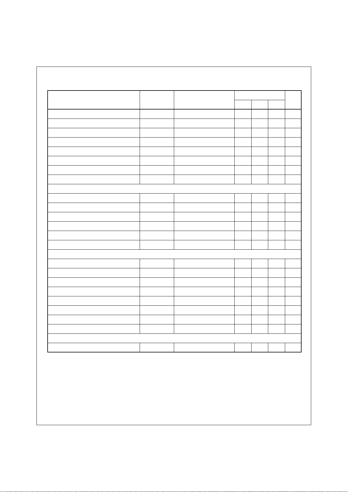
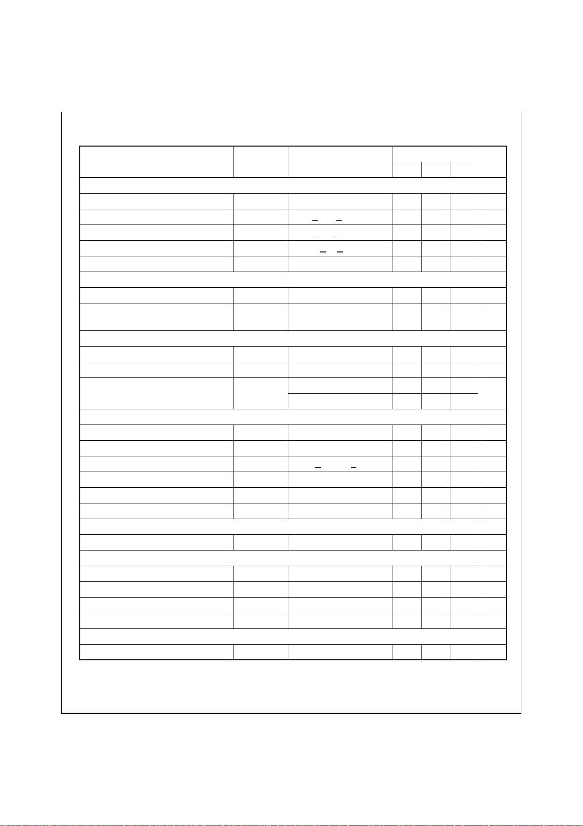
ELECTRICAL CHARACTERISTICS
5.
(continued)
Value
Characteristic Symbol Test Condition
Over voltage protection for 5V V
Over voltage protection for 12V V
Input threshold voltage for PT V
Under voltage protection for 3.3V V
Under voltage protection for 5V V
Under voltage protection for 12V V
Charging current for UVP delay I
CHG.UVP
UVP Delay Time T
OVP2
OVP3
PT
– 2.1 2.3 2.5 V
UVP1
UVP2
UVP3
C=2.2µF, VTH =1.8V -10 -15 -23 uA
D.UVP
C=2.2µF 100 260 500 ms
– 5.8 6.2 6.6 V
– 13.5 14.2 15.0 V
– 1.20 1.25 1.30
– 3.7 4.0 4.3 V
– 9.2 10 10.8 V
REMOTE ON/OFF SECTION
I
REM on input voltage V
REM off input voltage V
REM off input bias voltage I
REM on open voltage V
REM(OPEN)
REMH
REML
REML
= -200µA 2.0 – – V
REM
– – – 0.8 V
V
=0.4V – – -1.6 mA
REM
– 2.0 – 5.25 V
REM on delay time Ton C=0.1µF 4 8 14 ms
REM off delay time Toff C=0.1µF 16 24 34 ms
REMOTE ON/OFF SECTION
Detecting input voltage V
Detecting V5 voltage V
(2)
IN(DET)
5(DET)
– 1.20 1.25 1.30 V
– 4.1 4.3 4.5 V
Hysteresis voltage 1 HY1 COMP1, 2 10 40 80 mV
Hysteresis voltage 2 HY2 COMP3 0.6 1.2 – V
PG output load resistor R
Charging current for PG delay I
CHG.PG
PG delay time T
PG output saturation voltage V
SAT(PG) IPG
PG
D.PG
C=2.2µF, VTH =1.8V -10 -15 -23 uA
C=2.2µF 100 260 500 ms
– 0.5 1 2 k
=10mA – 0.4 0.2 V
TOTAL DEVICE
Standby supply current I
CC
–– 10 20 mA
Unit Min. Typ. Max.
Ω
Notes:
1. These Parameters, although guaranteed over their recommended operating conditions are not 100%
tested in production.
2. REM on delay time (Pin6 REM: “L” → “H”),
REM off delay time (Pin6 REM: “H” → “L”)
Rev C, November 1999
7

6. BLOCK DESCRIPTION & APPLICATION INFORMATIONS
6.1 OSCILLATOR BLOCK
Vref V
12
R
T
C
T
12
Figure 1. Oscillator RT, C
12 1
CC
T
The KA3511 is a fixed-frequency pulse width modulation control circuit. An internal-linear sawtooth
oscillator is fre quency-programmable by two external c omponents, R
and CT. The oscillator fre-
T
quency is determined by
1.1
fosc
300K
100K
10K
-------------------- -=
R
TCT
×
VCC=15V
0.001µF
CT=0.01µF
1K
- OSCILLATOR FREQUENCY
O
I
100
30
2K 5K 10K 20K 50K 100K 200K 500K 1M
1K
R
T
0.1µF
1.0µF
. TIMING RESISTANCE( Ω)
Figure 2. Oscillator Frequency vs. Timing Resistance
6.2 PWM CONTROL BLOCK
Output pulse width modu latio n is accompl ished by co mparis on of the pos itive sa wtooth wavefo rm
across capacitor C
Q1 and Q2, are enabled only when the flip-flop clock-input line is in its low state. This happens only
during that portion of time when the sawtooth voltage is greater than the control signals. Therefore,
an increase in control-signal amplitude c auses a corresponding linear d ecrease of output pulse
width. (Refer to the timing diagram shown in Figure 4)
to either of two control signals . T he NOR gate s, whi ch dr iv e outp ut trans is to rs
T
Rev C, November 1999
8
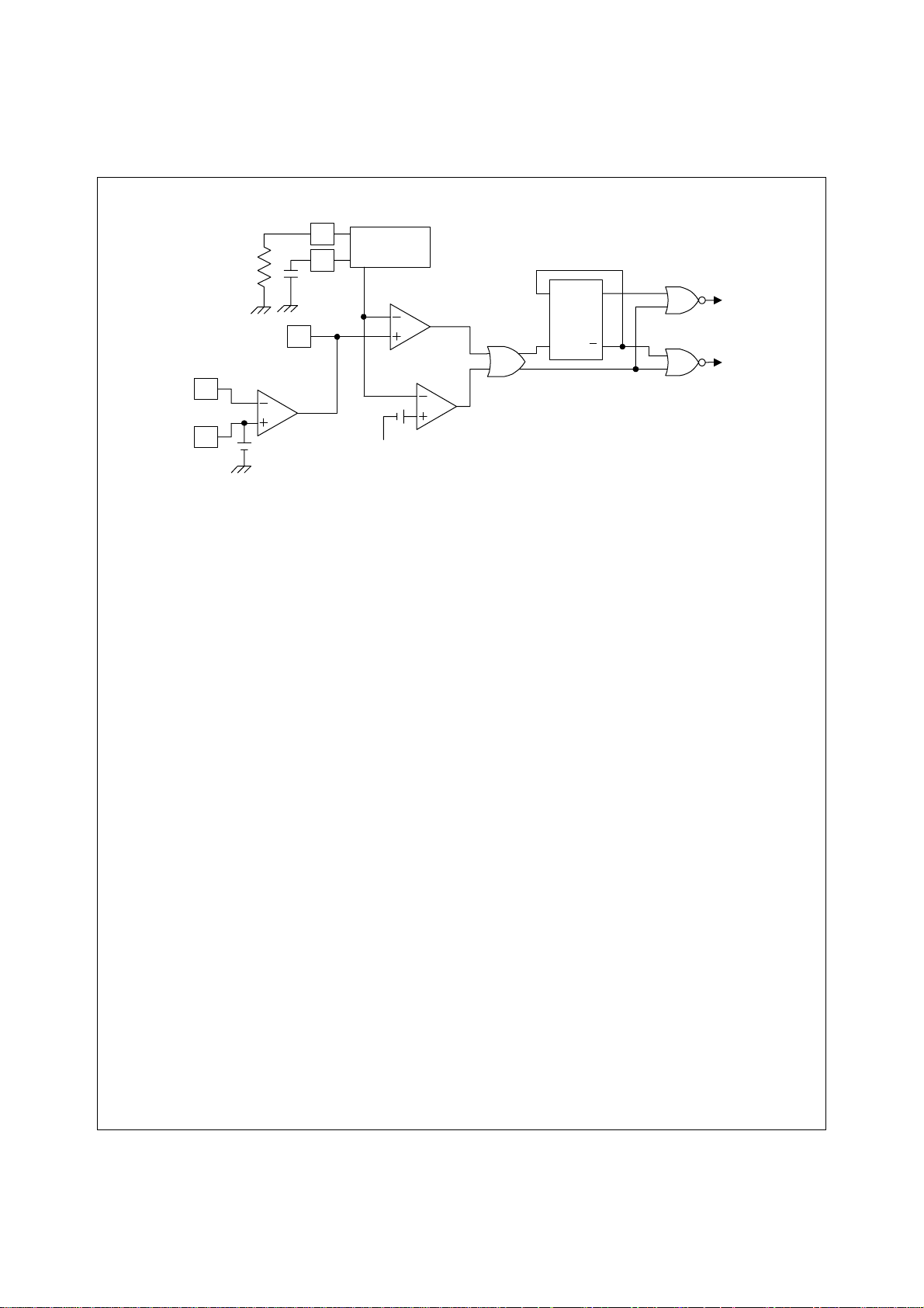
R
T
7
8
OSCILLATOR
DQ
Output
Drive
Q1
C
T
2
COMP
4
3
1.25V
PWM
CONTROL
0.12V
DEAD TIME
CONTROLLER
CK
Q
Q2
Figure 3. PWM Control Block
The control signals are external inputs that can be fed into the dead-time control, the error amplifier
inputs, or the feedbac k inp ut. The de ad-ti me contr ol com parator has an effective 120m V inp ut offset which limits the mi nimum output de ad time. Dead time m ay be impose d on the output by s etting the dead time control input to a fixed voltage, ranging between 0V to 3.3V.
The pulse width modulator comparator provides a means for the error amplifier to adjust the output
pulse width from the max imum percent on-ti me, established by the dead time control input, dow n
to zero, as the voltage at the feedb ack pin varies from 0.5V to 3.5V. The error amplifier may b e
used to sense powe r-supply output voltage, and its output is conn ect to noninve rting input of th e
pulse width modula tor comparator. With this configuration, the amplifier that demands minimum
output on time, dominates control of the loop.
When capacitor C
is discharged, a positive pulse is generated on the output of the dead time
T
comparator, which clocks the pulse-steering flip-flop and inhibits the output transistors, Q1 and Q2.
The pulse-steering flip-flop directs the modulated pulses to each of the two output transistors
always for push-pull operation. The output frequency is equal to half that of the oscillator.
The KA3511 has an internal 5.0V refer ence capable of sourcing u p to 10mA of load current for
external bias circui ts. The reference has an internal accuracy of ±2% with typical thermal dr ift of
less than 50mV over an operating temperature range of -25°C to 85°C
Rev C, November 1999
9
 Loading...