Fairchild Semiconductor KA3501 Datasheet

KA3501
PC SMPS Super visory IC
www.fairchildsemi.com
Features
• Complete House Keeping Circuit
• Few External Components
• Positive Voltage Protection
• Negative Voltage Protection
• High Current Drive Output for SCR
• Precision Voltage Reference for 5V/12V Outputs
• Power Good Signal Generat or with Hyster e sis
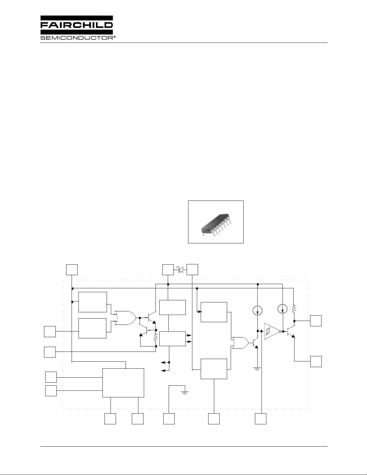
Internal Block Diagram
4
V
CC
1(+5V)
V
CC
Description
The KA3501 is complete housekeeping circuits for use in the
secondary side of SMPS(Switched Mode Power Supply).
This IC(Integrated Circuit) contains a precision voltage
reference, pr ot ection circuits and a power go od signal
generator. It also has a high current drive output for use in
conjunction with an external "crowbar" SCR. The reference
voltage is trimmed to ±2% for correct output voltages(+5V/
+12V) and power good signal generator is to monitor the
voltage level of power good supply for safe operation in a
microprocessor circuit. Using the KA3501 requires few
external components to accomplish a complete
housekeeping circuit for SMPS(Switched Mode Power
Supply). The KA3501 is available in an 14-pin DIP.
14-DIP
1
7
8
Vin1
Positive
Voltage
Protection
Vin2
5
GATE
6
Feedback
14
2
Vref
©2002 Fairchild Semiconductor Corporation
Negative
Voltage
Protection
V
CC
2(+12V)
+2.5V
REFERENCE
VOLTAGE
3
1
Vcont
START UP
INTERNAL
BIAS
13
GND
+5V
Detecting
COMP
V
CC
Detecting
COMP
9
Td
lchg
10
11
PG
12
Ve
Timing
Rev. 1.0.2

KA3501
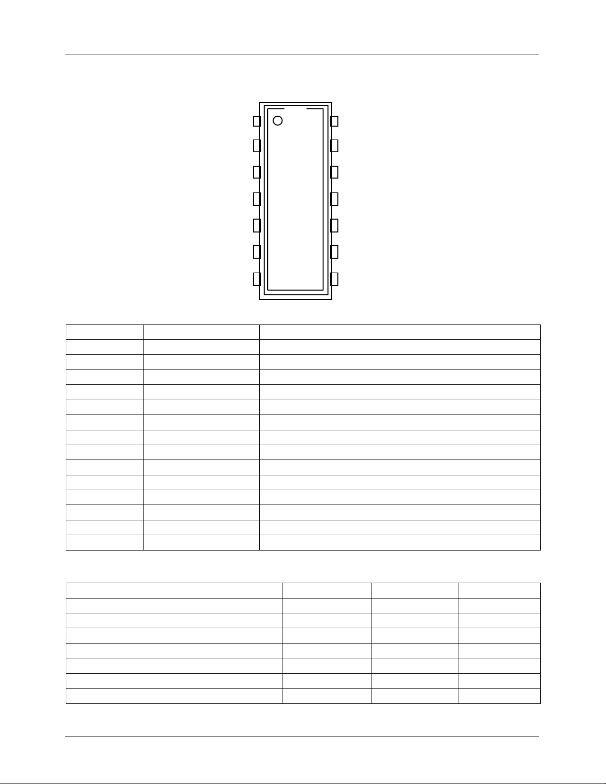
Pin Assignments
#14
Feedback
GND
Ve
Vcont
Vref
Vcc2
#1
K
A
Vcc1
3
PG
5
Vin2
0
Tim ing
1
Gate
Vcc
#7 #8
Pin Number Pin Name Pin Function Description
1 Vcont Reference Voltage Control
2 Vref Precision Reference Voltage
3 Vcc2 +12V Output Voltage
4 Vcc1 +5V Output Voltage
5 Vin2 UVP Input (Negative)
6 Gate Gate Drive Input for SCR
7 Vcc Supply Voltage
8 Vin1 PG Input
9 Td Reference Voltage Delay for PG
10 Timing PG Delay
11 PG PG Output
12 Ve PG Ground (Open Emitter)
13 GND Ground
14 Feedback Feedback for Precision Reference
Td
Vin1
Absolute Maximum Rating ( Ta = 25°°°°C)
Parameter Symbol Value Unit
Supply Minimum Voltage Vcc(min) 5 V
Supply Maximum Voltage Vcc(max) 35 V
UV Input Voltage Vuv 24 V
Minimum Gate Drive Current I
Operating Cathode Current I
Power Dissipation Pd 1 W
Operating Temperature Range Topr 0 to 70 °C
2
DR
K
-25 V
1 to 30 A
