

Fairchild Semiconductor KA350 Datasheet
www.fairchildsemi.com
KA350
3-Terminal 3A Positive Adjustable Voltage
Regulator
Features
• Output adjustable betwe en 1.2V an d 33V
• Guaranteed 3A output current
• Internal thermal over load protection
• Load regulation (Typ: 0.1%)
• Line regulation (Typ: 0.015%/V)
• Internal short circuit current limit
• Output transistor safe area compensation
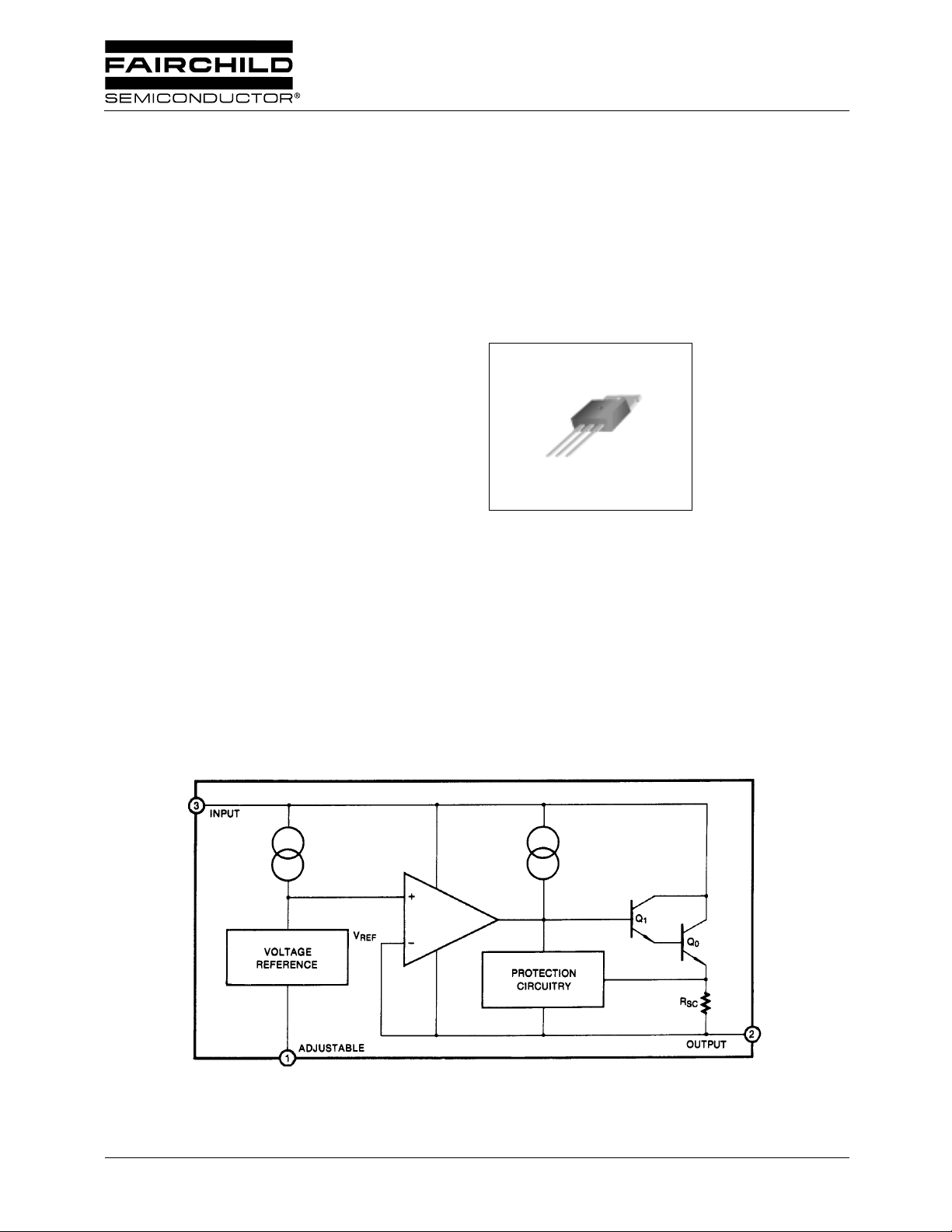
Internal Block Diagram
Description
The KA350 is an adjustable 3-terminal positive voltage
regulator capable of supplying in excess of 3.0 A over an
output voltage range of 1.2V to 33 V
TO-220
1
1. Adj 2. Output 3. Input
©2001 Fairchild Semiconductor Corporation
Rev. 1.0.0
KA350
Absolute Maximum Ratings
Parameter Symbol Value Unit
Input Output Voltage Differential V
Lead Temperature (Soldering, 10sec) T
I
LEAD
Power Dissipation P
Operating Temperature Range T
Storage Temperature Range T
- V
D
OPR
STG
O
35 V
300 °C
Internally limited -
0 ~ +125 °C
-65 ~ +150 °C
Electrical Characteristics
(VI-VO=5V, IO=1.5A, TJ=0°C to + 125°C; P
D
≤
P
, unless otherwise specified)
DMAX
DC
Parameter Symbol
Line Regulation (Note1) Rline T
Load Regulation (Note1)
Adjustment Pin Current I
Adjustment Pin Current
Change
Thermal Regulation REG
Reference Voltage V
Rload
ADJ
∆I
ADJ
REF
T
= +25°C, 3V ≤ VI -V
A
T
= +25
A
V
≤ 5V
O
V
≥ 5V
O
3V ≤ VI -V
10mA ≤ I
Pulse = 20ms, TA =+ 25°C - 0.002 - %/W
3V ≤ VI -V
Line Regulation Rline 3.0V ≤ V
Load Regulation
Rload
Temperature Stability ST
Maximum Output
Current
Minimum Load Current I
RMS Noise, %of V
OUT
Ripple Rejection
Long-Term Stability
I
o(MAX)
L(MIN)VI
V
RR
ST
10mA ≤ I
V
≤ 5.0V
O
V
≥ 5.0V
O
TJ = 0°C to + 125°C-1.0-%
T
VI -V
O
-VO = 30V, P
V
I
-VO = 35V - 3.5 10 mA
10Hz ≤ f ≤ 10KHz, TA= +25
N
V
= 10V, f = 120Hz,
O
C
= 0
ADJ
C
= 10µF66
ADJ
T
=+125
J
Conditions
°C, 3V ≤ V
≤ 35V,
O
≤ 3A, PD ≤ P
o
≤ 35V, 10mA ≤ I
O
≤ 35V - 0.02 0.07 %/W
I -VO
≤ 3.0A
O
≤ 10V, PD ≤ P
≤ P
D
°C
Min. Typ. Max. Unit
≤ 35V - 0.015 0.03 %/V
O
≤ 35V
I -VO
-5
0.1250.5
- - 50 100 µA
0.2 5.0 µA
MAX
O
≤ 3A,P
≤ 30W 1.2 1.25 1.30 V
D
-
-20
0.3701.5
MAX
MAX,TA
= +25°C 0.25 1.0 - A
°C - 0.003 - %/V
3.0 4.5 - A
65
-dB
80
0.3 1 %/
1000HR
mV
%
mV
%
o
dB
Note:
1. Regulation is measured at constant junction temperature. Changes in output voltage due to heating effects must be taken
into account separately. Pulse testing with low duty cycle is used.
2
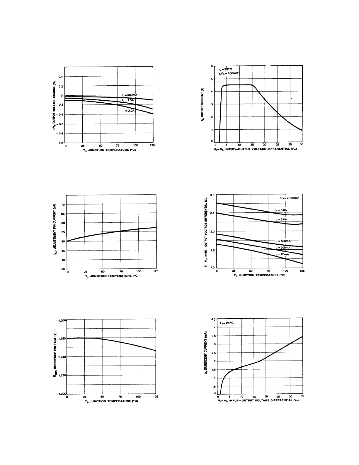
Typical Perfomance Characteristics
KA350
Figure 1. Load Regulation
Figure 3. Adjustment Pin Current
Figure 2. Current Limit
Figure 4. Dropout Voltage
Figure 5. Temperature Stability
Figure 6. Minimum Load Current
3
 Loading...