

Fairchild Semiconductor KA34063AD, KA34063A Datasheet
KA34063A
SMPS Controller
www.fairchildsemi.com
Features
• Operation From 3.0 to 40V In put
• Short Circuit Current L i miting
• Low Stand-by Current
• Output Switch Current of 1.5A Without External
Transistors
• Output Voltage Adjustable
• Frequency of Operation From 100Hz to 100kHz
• Step-up, Step-Down or Inverting Switching Regulators
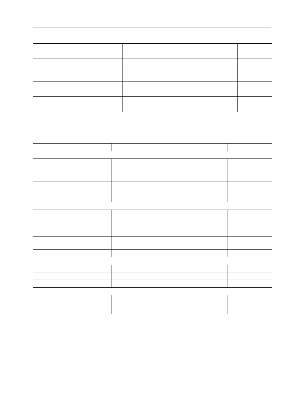
Internal Block Diagram
Description
The KA34063A is a monolithic regulator sub system
intended for use as DC to DC converter. This device
contains a temperature compensated bandgap reference, a
duty cycle control oscillator, a driver, and a high current
output switch. It can be used for step down, step up or
inverting switching regulators as well as for series pass
regulators.
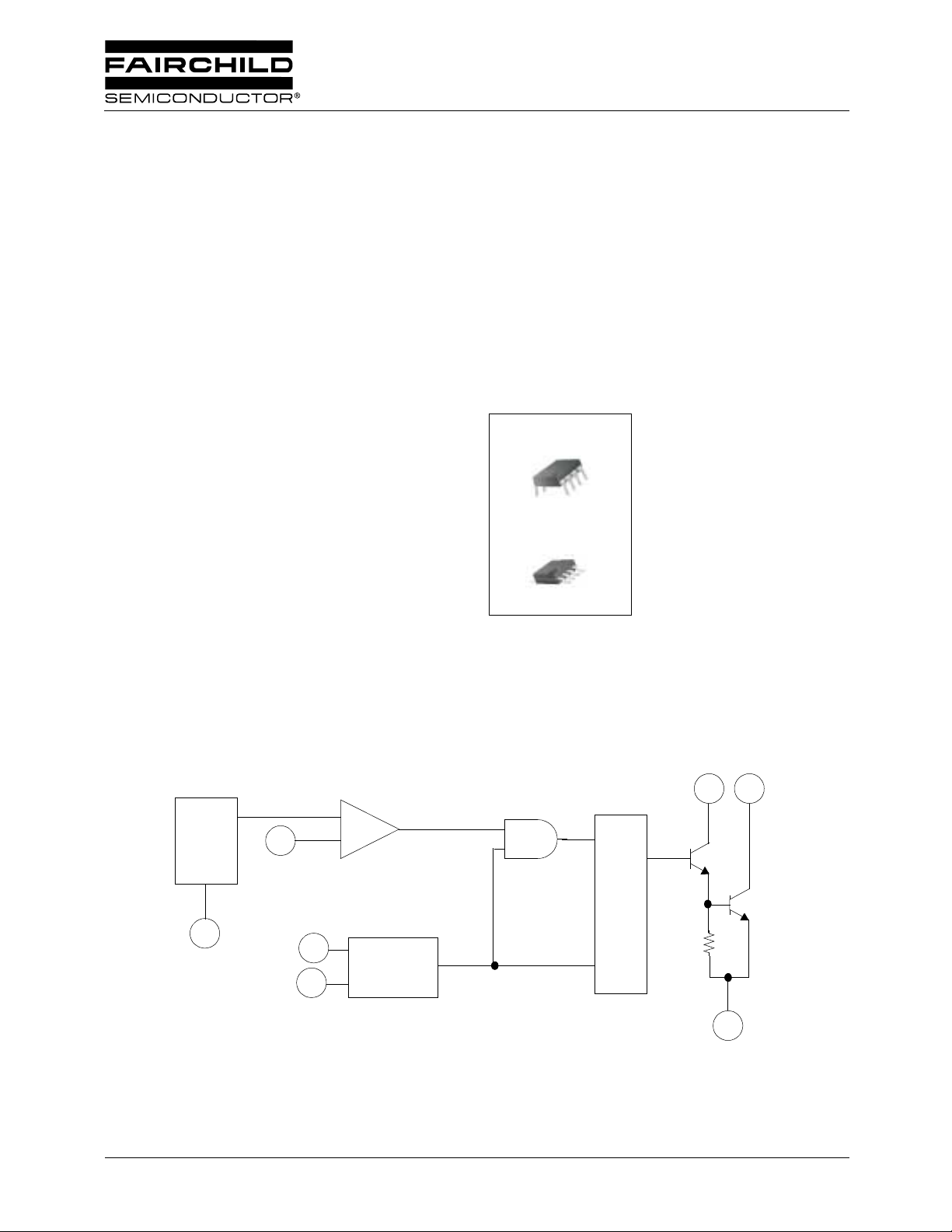
8-DIP
1
8-SOP
1
1.25V
REF
VTG
4
GND
* VCC(6)
©2002 Fairchild Semiconductor Corporation
5
COMPARATOR
INVERTING
INPUT
SENSE
I
PK
TIMING
CAPACITOR
7
3
COMP
OSCILLATOR
8
Q2
SWITCH
COLLECTOR
1
Q1
RD
DRIVE
COLLECTOR
S
Q
R
2
Rev. 1.0.1
KA34063A
Absolute Maximum Ratings
Parameter Symbol Value Unit
Supply Voltage V
Comparator Input Voltage Range V
I(COMP)
Switch Collector Voltage V
Switch Emitter Voltage V
Switch Collector To Emitter Voltage V
CE(SW)
Driver Collector Voltage V
Switch Current I
Storage Temperature Range T
CC
C(SW)
E(SW)
C(DR)
SW
STG
40 V
-0.3 ~ +40 V
40 V
40 V
40 V
40 V
1.5 A
-65 ~ +150 °C
Electrical Characteristics
(VCC = 5.0V, TA = 0°C to +70°C , unless otherwise specified)
Parameter Symbol Conditions Min. Typ. Max. Unit
OSCILLATOR
Charging Current I
Discharging Current I
Oscillator Amplitude V
CHG
DISCHG
(OSC)
Discharge to Charge Current Ratio K V
Current Limit Sense Voltage V
SENSE(C.L)
OUTPUT SWITCH
Saturation Voltage 1 (Note1) V
Saturation Voltage 2 (Note1,2) V
DC Current Gain (Note1,2) G
Collector off State Current (Note1) I
CE(SAT)
CE(SAT)
I(DC)
C(OFF)
COMPARATOR
Threshold Voltage V
Threshold Voltage Line Regulation ∆V
Input Bias Current I
TH
TH
BIAS
TOTAL DEVICE
Supply Current I
CC
VCC = 5 to 40V, TA = 25°C223142µA
VCC = 5 to 40V, TA = 25°C 140 190 260 µA
TA = 25°C0.5-V
I
CHG
TA = 25°C
I
SW
1
V
I
SW
2
V
ISW = 1.0A,
V
= V
7
= I
= 1.0A
(driver) = VC(SW)
C
= 1.0A,
(driver) = 50mA
C
= 5.0V, TA = 25°C
CE
= 25°C 5.2 6.1 7.5 -
CC, TA
DISCHG
250 300 350 mV
- 0.95 1.3 V
- 0.45 0.7 V
50 180 - -
VCE = 40V, TA = 25°C - 0.01 100 µA
- 1.21 1.24 1.29 V
VCC = 3 to 40V - 2.0 5.0 mV
VI = 0V - 50 400 nA
VCC = 5 to 40V, CT = 0.001uF
V
= V
7
CC, V5>VTH
-2.74.0mA
pin2 = GND
Note :
1. Output switch tests are performed under pulsed conditions to minimize power dissipation.
2. These parameters, although guaranteed, are not 100% tested in production.
2
 Loading...