

Fairchild Semiconductor KA1L0880B Datasheet
KA1L0880B/KA1M0880B
Fairchild Power Switch(FPS)
www.fairchildsemi.com
Features
• Precision fixed operating frequency
• KA1L0880B(50KHz),KA1M0880B(67KHz)
• Pulse by pulse over current limiting
• Over load protection
• Over voltage protection (Min. 23V)
• Internal thermal shutdown function
• Under voltage lock out
• Internal high voltage sense FET
• Latch up mode
•Soft start
Description
The Fairchild Power Switch(FPS) product family is specially
designed for an off-line SMPS with minimal external
components. The Fairchild Power Switch(FPS) consist of high
voltage power SenseFET and current mode PWM controller IC.
PWM controller features integrated fixed oscillator, under
voltage lock out, leading edge blanking, optimized gate turn-on/
turn-off driver , thermal shut down protection, over voltage
protection, temperature compensated precision current sources
for loop compensation and fault protection circuit. compared to
discrete MOSFET and controller or R
solution, a Fairchild Power Switch(FPS) can reduce total
component count, design size, weight and at the same time
increase & efficiency, productivity, and system reliability. It has
a basic platform well suited for cost effective design in either a
flyback converter or a forward converter.
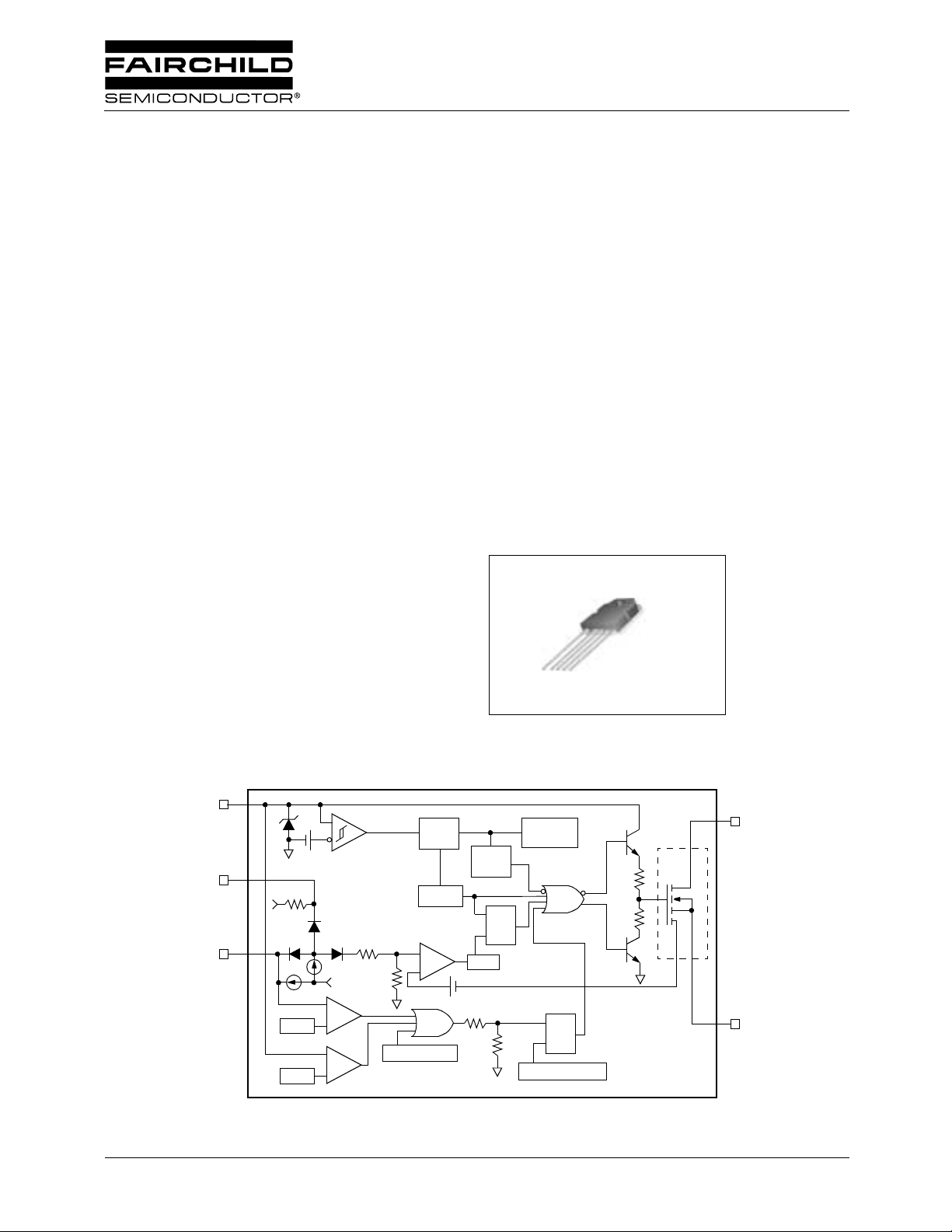
TO-3P-5L
1
1. DRAIN 2. GND 3. V
4. FB 5. S/S
CC
switching converter
CC
Internal Block Diagram
#3 V
CC
32V
#5 Soft Start
5V
#4 FB
©2001 Fairchild Semiconductor Corporation
µ
5
7.5V
25V
A
2.5R
1mA
1R
9V
+
−
+
−
Thermal S/D
OVER VOLTAGE S/D
OSC
−
+
5V
Vref
L.E.B
0.1V
Good
logic
S
R
Internal
bias
Q
S
R
Power on reset
#1 DRAIN
SFET
Q
#2 GND
Rev.1.0.2

KA1L0880B/KA1M0880B
Absolute Maximum Ratings
Parameter Symbol Value Unit
Maximum Drain voltage
Drain-Gate voltage (R
(1)
=1MΩ)V
GS
Gate-source (GND) voltage V
(4)
(2)
(3)
=25°C) I
C
Drain current pulsed
Single pulsed avalanche energy
Avalanche current
Continuous drain current (T
Continuous drain current (TC=100°C) I
Maximum Supply voltage V
Input voltage range V
Total power dissipation
Operating ambient temperature T
Storage temperature T
Notes:
1. Tj=25°C to 150°C
2. Repetitive rating: Pulse width limited by maximum junction temperature
3. L=24mH, V
4. L=13µH, starting Tj=25°C
=50V, RG=25Ω, starting Tj=25°C
DD
V
D,Max
DGR
GS
I
DM
E
AS
I
AS
D
D
CC,MAX
FB
P
D
800 V
800 V
±30 V
32.0 A
810 mJ
15 A
8.0 A
5.6 A
30 V
−0.3 to V
SD
190 W
Derating 1.54 W/°C
A
STG
−25 to +85 °C
−55 to +150 °C
DC
DC
DC
V
2

KA1L0880B/KA1M0880B
Electrical Characteristics (SFET part)
(Ta=25°C unless otherwise specified)
Parameter Symbol Condition Min. Typ. Max. Unit
Drain source breakdown voltage BV
Zero gate voltage drain current I
Static drain source on resistance
Forward transconductance
(note)
(note)
DSS
DSS
R
DS(ON)
gfs VDS=15V, ID=5.0A 1.5 2.5 - S
Input capacitance Ciss
Reverse transfer capacitance Crss - 64 Turn on delay time t
d(on)
Rise time tr - 95 200
Turn off delay time t
d(off)
Fall time tf - 60 150
Total gate charge
(gate-source+gate-drain)
Qg
Gate source charge Qgs - 20 Gate drain (Miller) charge Qgd - 70 -
VGS=0V, ID=50µA 800 - - V
VDS=Max., Rating,
V
=0V
GS
=0.8Max., Rating,
V
DS
V
=0V, TC=125°C
GS
--50µA
- - 200 µA
VGS=10V, ID=5.0A - 1.2 1.5 Ω
- 2460 -
=0V, VDS=25V,
V
GS
f=1MHz
VDD=0.5BV
DSS
, ID=8.0A
--90
(MOSFET switching
time are essentially
independent of
- 150 450
operating temperature)
V
=10V, ID=8.0A,
V
GS
DS
=0.5BV
(MOSFET
DSS
- - 150
switching time are
essentially independent of
operating temperature)
pFOutput capacitance Coss - 210 -
nS
nC
Note:
Pulse test: Pulse width ≤ 300µS, duty cycle ≤ 2%
1
S
--- -=
R
3
 Loading...