

Fairchild Semiconductor HGTG11N120CN Datasheet
HGTG11N120CN, HGTP11N120CN,
HGT1S11N120CNS
Data Sheet December 2001
43A, 1200V, NPT Series N-Channel IGBT
The HGTG11N120CN, HGTP11N120CN, and
HGT1S11N120CNS are Non-Punch Through ( NPT) IGBT
designs. They are new members of the M OS gate d high
voltage switching IGBT family. IGBTs combine the best
features of MO SFETs and bipolar transistors. This device
has the high input impedance of a MOSFET and the low onstate conduction loss of a bipolar transistor.
The IGBT is ideal for many high vol tag e switching
applications operating at moderate frequenci es w here low
conduction losses are essential, such as: AC and DC motor
controls, power supplies and drivers for solenoids, relays
and contactors.
Formerly Developmental Type TA49291.
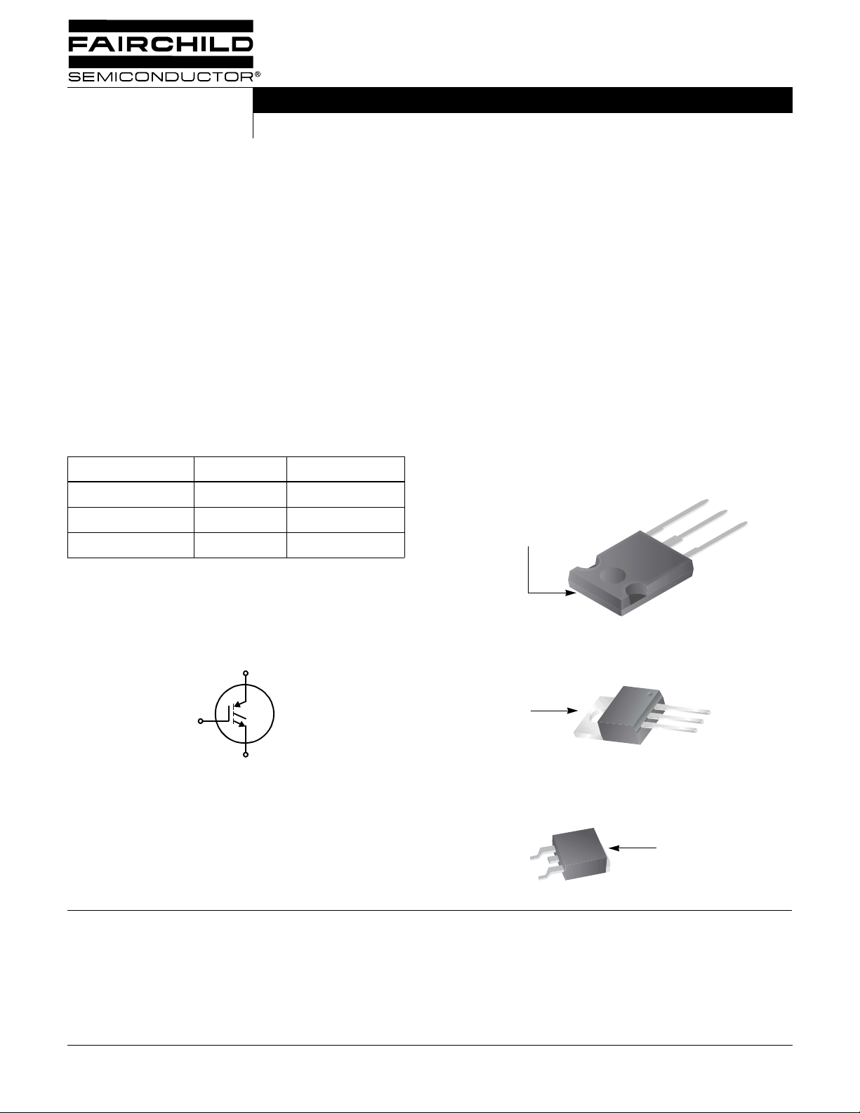
Ordering Information
PART NUMBER PACKAGE BRAND
HGTG11N120CN TO-247 G11N120CN
HGTP11N120CN TO-220AB 11N120CN
HGT1S11N120CNS TO-263AB 11N120CN
NOTE: When ordering, use the entire part number. Add the suffix 9A
to obtain the TO-263AB variant in Tape and Reel, i.e.,
HGT1S11N120CNS9A.
Features
• 43A, 1200V, TC = 25oC
• 1200V Switching SOA Capability
• Typical Fall Time. . . . . . . . . . . . . . . . 340ns at T
• Short Circuit Rating
• Low Conduction Loss
• Avalanche Rated
• Thermal Impedance SPICE Model
Temperature Compensating SABER™ Model
www.fairchildsemi.com
• Related Literature
- TB334 “Guidelines for Soldering Surface Mount
Components to PC Boards”
Packaging
JEDEC STYLE TO-247
E
COLLECTOR
(BOTTOM SIDE
METAL)
= 150oC
J
C
G
Symbol
C
COLLECTOR
G
E
FAIRCHILD SEMICONDUCTOR IGBT PRODUCT IS COVERED BY ONE OR MORE OF THE FOLLOWING U.S. PATENTS
4,364,073 4,417,385 4,430,792 4,443,931 4,466,176 4,516,143 4,532,534 4,587,713
4,598,461 4,605,948 4,620,211 4,631,564 4,639,754 4,639,762 4,641,162 4,644,637
4,682,195 4,684,413 4,694,313 4,717,679 4,743,952 4,783,690 4,794,432 4,801,986
4,803,533 4,809,045 4,809,047 4,810,665 4,823,176 4,837,606 4,860,080 4,883,767
4,888,627 4,890,143 4,901,127 4,904,609 4,933,740 4,963,951 4,969,027
JEDEC TO-220AB (ALTERNATE VERSION)
(FLANGE)
JEDEC TO-263AB
COLLECTOR
G
E
(FLANGE)
E
C
G
©2001 Fairchild Semiconductor Corpo ration HGTG11N120CN, HGTP11N120CN, HGT1S11N120CNS Rev. B
HGTG11N120CN, HGTP11N120CN, HGT1S11N120CNS
Absolute Maximum Ratings
TC = 25oC, Unless Otherwise Specified
HGTG11N120CN
HGTP11N120CN
HGT1S11N120CNS UNITS
Collector to Emitter Voltage . . . . . . . . . . . . . . . . . . . . . . . . . . . . . . . . . . . . . . . . . . . . . . BV
CES
1200 V
Collector Current Continuous
= 25oC . . . . . . . . . . . . . . . . . . . . . . . . . . . . . . . . . . . . . . . . . . . . . . . . . . . . . . . . . I
At T
C
= 110oC . . . . . . . . . . . . . . . . . . . . . . . . . . . . . . . . . . . . . . . . . . . . . . . . . . . . . . . I
At T
C
Collector Current Pulsed (Note 1) . . . . . . . . . . . . . . . . . . . . . . . . . . . . . . . . . . . . . . . . . . . I
Gate to Emitter Voltage Continuous. . . . . . . . . . . . . . . . . . . . . . . . . . . . . . . . . . . . . . . . . V
Gate to Emitter Voltage Pulsed . . . . . . . . . . . . . . . . . . . . . . . . . . . . . . . . . . . . . . . . . . . . V
Switching Safe Operating Area at T
Pow er Dissi pation Total at T
C
Power Dissipation Derating T
= 150oC (Figure 2) . . . . . . . . . . . . . . . . . . . . . . . SSOA 55A at 1200V
J
= 25oC . . . . . . . . . . . . . . . . . . . . . . . . . . . . . . . . . . . . . . . . . P
> 25oC . . . . . . . . . . . . . . . . . . . . . . . . . . . . . . . . . . . . . . . . . . 2.38 W/oC
C
Forward Voltage Avalanche Energy (Note 2). . . . . . . . . . . . . . . . . . . . . . . . . . . . . . . . . . . E
Operating and Storage Junction Tem perature Range . . . . . . . . . . . . . . . . . . . . . . . . T
, T
J
C25
C110
CM
GES
GEM
D
AV
STG
43 A
22 A
80 A
±20 V
±30 V
298 W
80 mJ
-55 to 150
o
C
Maximum Lead T emperature f or Soldering
Leads at 0.063in (1.6mm) from case for 10s . . . . . . . . . . . . . . . . . . . . . . . . . . . . . . . . . . T
Package Body for 10s, see Tech brief 334. . . . . . . . . . . . . . . . . . . . . . . . . . . . . . . . . . . T
Short Circuit Withstand Time (Not e 3) at V
Short Circuit Withstand Time (Not e 3) at V
CAUTION: Stresses above those listed in “A bsolute Maximu m Rating s” may cause per manent d amage to t he device. This is a str ess on ly rating and operation o f the
device at these or any other conditions above those indicated in the operational sections of this specification is not implied.
= 15V. . . . . . . . . . . . . . . . . . . . . . . . . . . . . .t
GE
= 12V. . . . . . . . . . . . . . . . . . . . . . . . . . . . . .t
GE
L
pkg
SC
SC
300
260
8 µs
15 µs
o
C
o
C
NOTES:
1. Pulse width limited by maximum junction temperature.
= 20A, L = 400µH, TJ = 25oC.
2. I
CE
3. V
= 840V, TJ = 125oC, RG = 10Ω.
CE(PK)
Electrical Specifications
TC = 25oC, Unless Otherwise Specified
PARAMETER SYMBOL TEST CONDITIONS MIN TYP MAX UNITS
Collector to Emitter Breakdown Voltage BV
Emitter to Collector Breakdown Voltage BV
Collector to Emitter Leakage Current I
Collector to Emitter Saturation Voltage V
Gate to Emitter Threshold Voltage V
Gate to Emitter Leakage Current I
CES
ECS
CES
CE(SAT)IC
GE(TH)
GES
Switching SOA SSOA T
Gate to Emitter Plateau Voltage V
On-State Gate Charge Q
GEP
G(ON)
IC = 250µA, VGE = 0V 1200 - - V
IC = 10mA, V
= 0V 15 - - V
GE
VCE = 1200V TC = 25oC - - 250 µA
T
= 125oC - 250 - µA
C
T
= 150oC--3mA
C
= 11A,
V
= 15V
GE
IC = 90µA, VCE = V
= 25oC-2.12.4V
T
C
T
= 150oC-2.83.5V
C
GE
6.0 6.8 - V
VGE = ±20V - - ±250 nA
= 150oC, RG = 10Ω, VGE = 15V,
J
L = 400µH, V
CE(PK)
= 1200V
55 - - A
IC = 11A, VCE = 600V - 10.4 - V
IC = 11A,
= 600V
V
CE
V
= 15V - 100 120 nC
GE
= 20V - 130 150 nC
V
GE
©2001 Fairchild Semiconductor Corpo ration HGTG11N120CN, HGTP11N120CN, HGT1S11N120CNS Rev. B

I
, DC COLLECTOR CURRENT (A)
0
0
I
, COLLECTOR TO EMITTER CURRENT (A)
HGTG11N120CN, HGTP11N120CN, HGT1S11N120CNS
Electrical Specifications
TC = 25oC, Unless Otherwise Specified (Continued)
PARAMETER SYMBOL TEST CONDITIONS MIN TYP MAX UNITS
Current Turn-On Delay Time t
d(ON)I
Current Rise Time t
Current Turn-Off Delay Time t
d(OFF)I
Current Fall Time t
Turn-On Energy (Note 4) E
Turn-On Energy (Note 4) E
Turn-Off Energy (Note 5) E
Current Turn-On Delay Time t
d(ON)I
Current Rise Time t
Current Turn-Off Delay Time t
d(OFF)I
Current Fall Time t
Turn-On Energy (Note 4) E
Turn-On Energy (Note 4) E
Turn-Off Energy (Note 5) E
Thermal Resistance Junction To Case R
rI
fI
ON1
ON2
OFF
rI
fI
ON1
ON2
OFF
θJC
IGBT and Diode at TJ = 25oC
= 11A
I
CE
= 960V
V
CE
V
= 15V
GE
= 10Ω
R
G
L = 2mH
Test Circuit (Figure 18)
IGBT and Diode at TJ = 150oC
= 11A
I
CE
V
= 960V
CE
= 15V
V
GE
= 10Ω
R
G
L = 2mH
Test Circuit (Figure 18)
NOTES:
4. Values for two Turn-On loss co nditions ar e shown for the convenience o f the circu it designer. E
is the turn-on loss when a typical diode is used in the test circuit and the diode is at the same T
Figure 18.
5. Turn-Off Energy Loss (E
at the point where the collector current equals zero (I
) is defined as the integral of the instantaneous power loss starting at the trailing edge of the input pulse and ending
OFF
= 0A). All devices were tested per JEDEC Standard No. 24-1 Method for Measurement
CE
of Power Device Turn-Off Switching Loss. This test met hod produces the true total Turn-Off Energy Loss.
-2326ns
-1216ns
- 180 240 ns
- 190 230 ns
-0.40.5mJ
-0.951.3 mJ
-1.31.6mJ
-2124ns
-1216ns
- 210 280 ns
- 340 400 ns
-0.450.6 mJ
-1.92.5mJ
-2.12.5mJ
- - 0.42
is the turn-on loss of the IGBT only. E
ON1
as the IGBT. The diode type is specifi ed in
J
o
C/W
ON2
Typical Performance Curves
45
40
35
30
25
20
15
10
5
CE
0
25 75 100 125 15
50
TC, CASE TEMPERATURE (oC)
Unless Otherwise Specified
FIGURE 1. DC COLLECTOR CURRENT vs CASE
TEMPERATURE
CE
60
50
TJ = 150oC, RG = 10Ω, V
40
30
20
10
0
0
V
= 15V, L = 400µH
GE
600 800400200 1000 1200
, COLLECTOR TO EMITTER VOLTAGE (V)
CE
140
V
= 15V
GE
FIGURE 2. MINIMUM SWITCHING SAFE OPERATING AREA
©2001 Fairchild Semiconductor Corpo ration HGTG11N120CN, HGTP11N120CN, HGT1S11N120CNS Rev. B
 Loading...