

Fairchild Semiconductor HGTD3N60C3S Datasheet
SEMICONDUCTOR
HGTD3N60C3,
HGTD3N60C3S
June 1997
Features
• 6A, 600V at TC = 25oC
• 600V Switching SOA Capability
• Typical Fall Time . . . . . . . . . . . . . . 130ns at T
• Short Circuit Rating
• Low Conduction Loss
= 150oC
J
Ordering Information
PART NUMBER PACKAGE BRAND
HGTD3N60C3 TO-251AA G3N60C
HGTD3N60C3S TO-252AA G3N60C
NOTE: When ordering, use the entire part number. Add the suffix 9A
to obtain the TO-252AA variant in Tape and Reel, i.e.
HGTD3N60C3S9A.
6A, 600V, UFS Series N-Channel IGBTs
Description
The HGTD3N60C3 and HGTD3N60C3S are MOS gated high
voltage switching devices combining the best features of
MOSFETs and bipolar transistors. These devices have the
high input impedance of a MOSFET and the low on-state conduction loss of a bipolar transistor. The much lower on-state
voltage drop varies only moderately between 25
o
150
C.
The IGBT is ideal for many high voltage switching
applications operating at moderate frequencies where low
conduction losses are essential, such as: AC and DC motor
controls, power supplies and drivers for solenoids, relays
and contactors.
Formerly developmental type TA49113.
Symbol
N-CHANNEL ENHANCEMENT MODE
C
o
C and
G
E
Packaging
JEDEC TO-251AA JEDEC TO-252AA
EMITTER
COLLECTOR
(FLANGE)
HARRIS SEMICONDUCTOR IGBT PRODUCT IS COVERED BY ONE OR MORE OF THE FOLLOWING U.S. PATENTS:
4,364,073 4,417,385 4,430,792 4,443,931 4,466,176 4,516,143 4,532,534 4,567,641
4,587,713 4,598,461 4,605,948 4,618,872 4,620,211 4,631,564 4,639,754 4,639,762
4,641,162 4,644,637 4,682,195 4,684,413 4,694,313 4,717,679 4,743,952 4,783,690
4,794,432 4,801,986 4,803,533 4,809,045 4,809,047 4,810,665 4,823,176 4,837,606
4,860,080 4,883,767 4,888,627 4,890,143 4,901,127 4,904,609 4,933,740 4,963,951
COLLECTOR
GATE
GATE
EMITTER
COLLECTOR
(FLANGE)
CAUTION: These devices are sensitive to electrostatic discharge. Users should follow proper ESD handling procedures.
Copyright
© Harris Corporation 1997
1
File Number 4139.3
HGTD3N60C3, HGTD3N60C3S
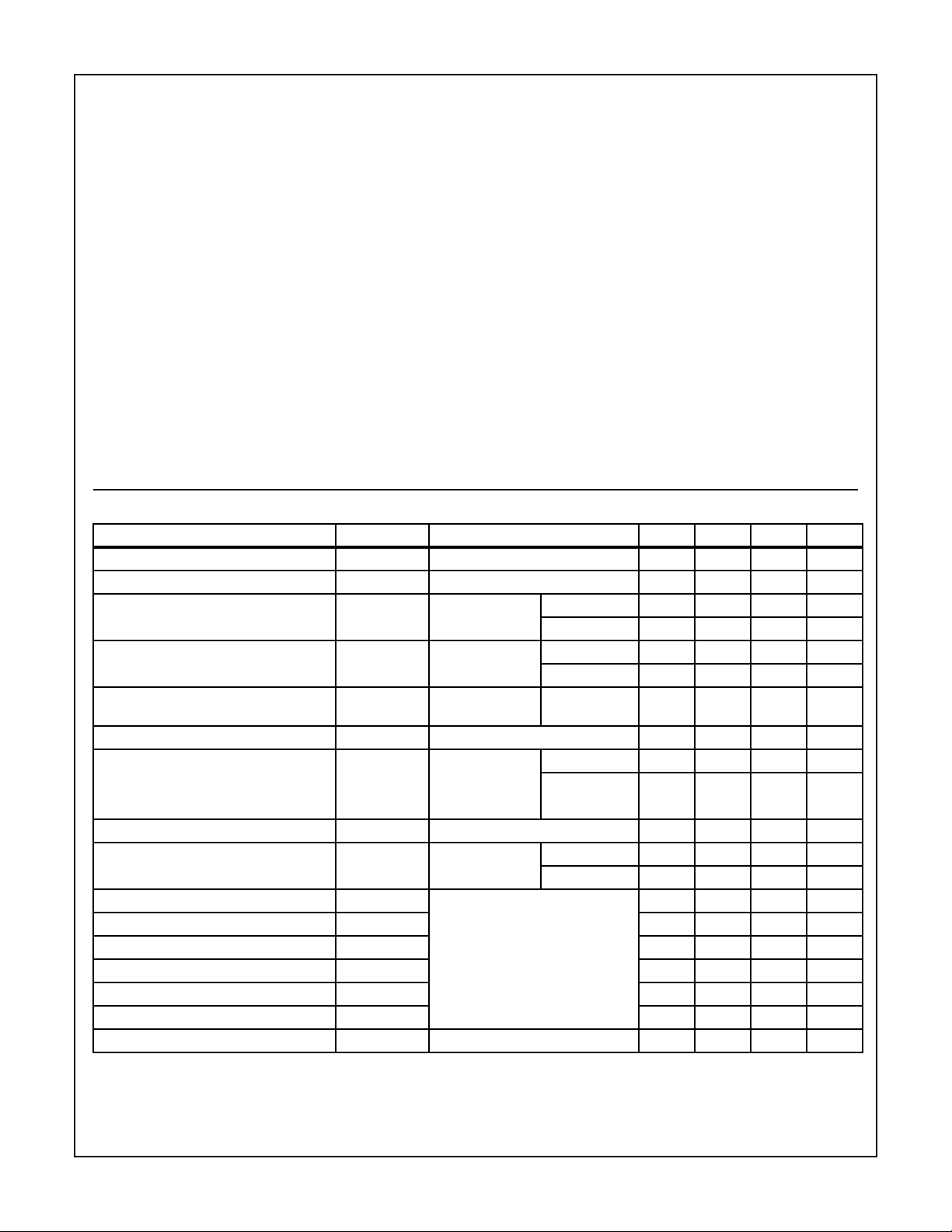
Absolute Maximum Ratings T
= 25oC
C
HGTD3N60C3
HGTD3N60C3S UNITS
Collector to Emitter Voltage . . . . . . . . . . . . . . . . . . . . . . . . . . . . . . . . . . . . . . . . . . . . . . BV
CES
600 V
Collector Current Continuous
At TC = 25oC . . . . . . . . . . . . . . . . . . . . . . . . . . . . . . . . . . . . . . . . . . . . . . . . . . . . . . . . . I
= 110oC . . . . . . . . . . . . . . . . . . . . . . . . . . . . . . . . . . . . . . . . . . . . . . . . . . . . . . . I
At T
C
C25
C110
Collector Current Pulsed (Note 1) . . . . . . . . . . . . . . . . . . . . . . . . . . . . . . . . . . . . . . . . . . . .I
Gate to Emitter Voltage Continuous. . . . . . . . . . . . . . . . . . . . . . . . . . . . . . . . . . . . . . . . . V
Gate to Emitter Voltage Pulsed . . . . . . . . . . . . . . . . . . . . . . . . . . . . . . . . . . . . . . . . . . . . V
Switching Safe Operating Area at T
Power Dissipation Total at T
Power Dissipation Derating T
= 150oC, Figure 14 . . . . . . . . . . . . . . . . . . . . . . . .SSOA 18A at 480V
J
= 25oC . . . . . . . . . . . . . . . . . . . . . . . . . . . . . . . . . . . . . . . . . P
C
> 25oC . . . . . . . . . . . . . . . . . . . . . . . . . . . . . . . . . . . . . . . . . . . 0.27 W/oC
C
Reverse Voltage Avalanche Energy. . . . . . . . . . . . . . . . . . . . . . . . . . . . . . . . . . . . . . . . . E
Operating and Storage Junction Temperature Range . . . . . . . . . . . . . . . . . . . . . . . . T
GES
GEM
ARV
, T
J
STG
Maximum Lead Temperature for Soldering . . . . . . . . . . . . . . . . . . . . . . . . . . . . . . . . . . . . . .T
Short Circuit Withstand Time (Note 2) at V
= 10V, Figure 6 . . . . . . . . . . . . . . . . . . . . . . t
GE
CM
D
L
SC
6A
3A
24 A
±20 V
±30 V
33 W
100 mJ
-40 to 150
260
8 µs
NOTES:
1. Repetitive Rating: Pulse width limited by maximum junction temperature.
2. V
Electrical Specifications T
= 360V, TJ = 125oC, RGE = 82Ω.
CE(PK)
= 25oC, Unless Otherwise Specified
C
PARAMETER SYMBOL TEST CONDITIONS MIN TYP MAX UNITS
Collector to Emitter Breakdown Voltage BV
Emitter to Collector Breakdown Voltage BV
Collector to Emitter Leakage Current I
CES
ECS
CES
IC = 250µA, VGE = 0V 600 - - V
IC = 3mA, VGE= 0V 16 30 - V
VCE = BV
CES
TC = 25oC - - 250 µA
TC = 150oC - - 2.0 mA
Collector to Emitter Saturation Voltage V
Gate to Emitter Threshold Voltage V
Gate to Emitter Leakage Current I
CE(SAT)IC
GE(TH)
GES
Switching SOA SSOA TJ = 150oC
= I
C110
VGE = 15V
IC = 250µA,
VCE = V
GE
,
TC = 25oC - 1.65 2.0 V
TC = 150oC - 1.85 2.2 V
TC = 25oC 3.0 5.5 6.0 V
VGE = ±25V - - ±250 nA
RG = 82Ω
VGE = 15V
V
V
= 480V 18 - - A
CE(PK)
= 600V 2 - - A
CE(PK)
L = 1mH
Gate to Emitter Plateau Voltage V
On-State Gate Charge Q
Current Turn-On Delay Time t
d(ON)I
Current Rise Time t
Current Turn-Off Delay Time t
d(OFF)I
Current Fall Time t
Turn-On Energy E
Turn-Off Energy (Note 3) E
Thermal Resistance R
GEP
g(ON)
rI
fI
ON
OFF
θJC
IC = I
IC = I
, VCE = 0.5 BV
C110
,
C110
VCE = 0.5 BV
TJ = 150oC
ICE = I
C110
V
= 0.8 BV
CE(PK)
VGE = 15V
RG= 82Ω
L = 1mH
CES
- 8.3 - V
VGE = 15V - 10.8 13.5 nC
CES
VGE = 20V - 13.8 17.3 nC
-5-ns
CES
-10-ns
- 325 400 ns
- 130 275 ns
-85-µJ
- 245 - µJ
- - 3.75
NOTE:
3. Turn-Off Energy Loss (E
) is defined as the integral of the instantaneous power loss starting at the trailing edge of the input pulse and
OFF
ending at the point where the collector current equals zero (ICE = 0A). The HGTD3N60C3 and HGTD3N60C3S were tested per JEDEC
standard No. 24-1 Method for Measurement of Power Device Turn-Off Switching Loss. This test method produces the true total Turn-Off
Energy Loss. Turn-On losses include diode losses.
o
C
o
C
o
C/W
2
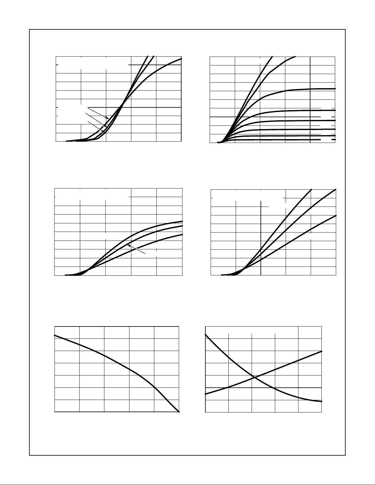
Typical Performance Curves
HGTD3N60C3, HGTD3N60C3S
20
DUTY CYCLE <0.5%, V
18
PULSE DURATION = 250µs
16
14
12
10
TC = 150oC
8
T
= 25oC
C
6
TC = -40oC
4
2
, COLLECTOR TO EMITTER CURRENT (A)
0
CE
I
4
6 8 10 12
VGE, GATE TO EMITTER VOLTAGE (V)
CE
= 10V
FIGURE 1. TRANSFER CHARACTERISTICS FIGURE 2. SATURATION CHARACTERISTICS
20
PULSE DURATION = 250µs
DUTY CYCLE <0.5%, V
18
16
14
12
10
8
6
4
2
, COLLECTOR TO EMITTER CURRENT (A)
CE
0
I
0123 45
, COLLECTOR TO EMITTER VOLTAGE (V)
V
CE
= 10V
GE
TC = -40oC
TC = 150oC
TC = 25oC
20
18
16
14
12
10
8
6
4
, COLLECTOR TO EMITTER CURRENT (A)
2
CE
I
14
0
20
18
16
14
12
10
8
6
4
2
, COLLECTOR TO EMITTER CURRENT (A)
0
CE
I
PULSE DURATION = 250µs, DUTY CYCLE <0.5%, T
VGE = 15V
0246810
VCE, COLLECTOR TO EMITTER VOLTAGE (V)
PULSE DURATION = 250µs
DUTY CYCLE <0.5%, VGE = 15V
TC = -40oC
012345
, COLLECTOR TO EMITTER VOLTAGE (V)
V
CE
12V
= 25oC
C
10V
9.0V
8.5V
8.0V
7.5V
7.0V
TC = 25oC
TC = 150oC
FIGURE 3. COLLECTOR TO EMITTER ON-STATE VOLTAGE FIGURE 4. COLLECTOR TO EMITTER ON-STATE VOLTAGE
7
V
= 15V
GE
6
5
4
3
2
, DC COLLECTOR CURRENT (A)
1
CE
I
0
25 50 75 100 125 150
TC, CASE TEMPERATURE (oC)
FIGURE 5. MAXIMUM DC COLLECTOR CURRENT AS A
14
VCE = 360V, RGE = 82Ω, TJ = 125oC
12
10
8
6
4
2
, SHORT CIRCUIT WITHSTAND TIME (µS)
SC
0
t
10 11 12
t
SC
V
, GATE TO EMITTER VOLTAGE (V)
GE
FIGURE 6. SHORT CIRCUIT WITHSTAND TIME
I
SC
14 1513
70
60
50
40
30
20
10
0
FUNCTION OF CASE TEMPERA TURE
3
, PEAK SHORT CIRCUIT CURRENT (A)
SC
I
 Loading...