

Fairchild Semiconductor HGT1N40N60A4D Datasheet
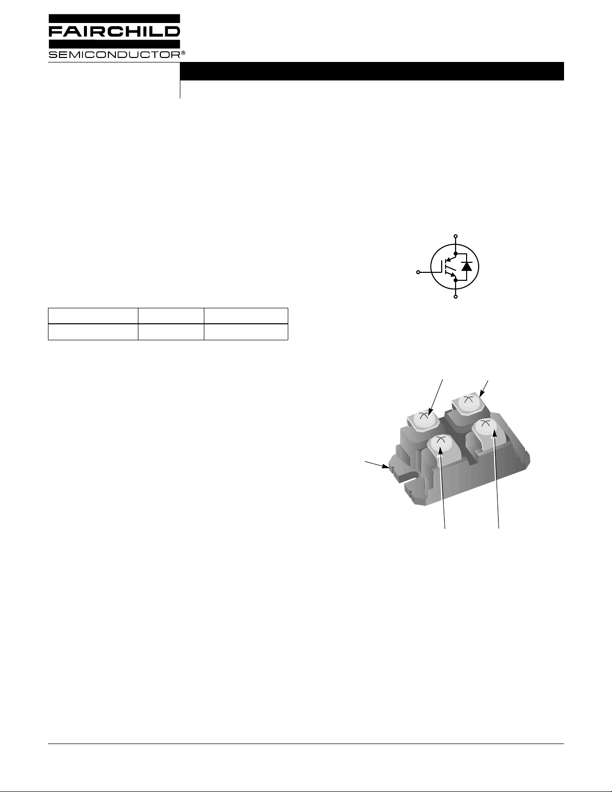
GATE
COLLECTOR
EMITTER
EMITTER
TAB
(ISOLATED)
HGT1N40N60A4D
Data Sheet December 2001
600V, SMPS Series N-Channel IGBT with
Anti-Parallel Hyperfast Diode
The HGT1N40N60A4D is a MOS gated high voltage
switching device combining the best features of a MOSFET
and a bipolar transistor. These devices have the high input
impedance of a MOSFET and the low on-state conduction
loss of a bipolar transistor. The much lower on-state voltage
drop varies only moderately between 25
o
C and 150
o
C. This
IGBT is ideal for many high voltage switching applications
operating at high frequencies where low conduction losses
are essential. This device has been optimized for high
frequency switch mode power supplies.
Formerly Developmental Type TA49349.
Ordering Information
PART NUMBER PACKAGE BRAND
HGT1N40N60A4D SOT-227 40N60A4D
NOTE: When ordering, use the entire part number.
Features
• 100kHz Operation At 390V, 22A
• 600V Switching SOA Capability
• Typical Fall Time. . . . . . . . . . . . . . . . . 55ns at T
• Low Conduction Loss
Symbol
C
G
E
Packaging
JEDEC STYLE SOT-227B
= 125
J
o
C
Fairchild CORPORATION IGBT PRODUCT IS COVERED BY ONE OR MORE OF THE FOLLOWING U.S. PATENTS
4,364,073 4,417,385 4,430,792 4,443,931 4,466,176 4,516,143 4,532,534 4,587,713
4,598,461 4,605,948 4,620,211 4,631,564 4,639,754 4,639,762 4,641,162 4,644,637
4,682,195 4,684,413 4,694,313 4,717,679 4,743,952 4,783,690 4,794,432 4,801,986
4,803,533 4,809,045 4,809,047 4,810,665 4,823,176 4,837,606 4,860,080 4,883,767
4,888,627 4,890,143 4,901,127 4,904,609 4,933,740 4,963,951 4,969,027
©2001 Fairchild Semiconductor Corporation HGT1N40N60A4D Rev. B
±
±
µ
±
µ
µ
µ
µ
µ
µ
HGT1N40N60A4D
Absolute Maximum Ratings
o
T
= 25
C, Unless Otherwise Noted
C
HGT1N40N60A4D UNITS
Collector to Emitter Voltage . . . . . . . . . . . . . . . . . . . . . . . . . . . . . . . . . . . . . . . . . . . . . .BV
CES
600 V
Collector Current Continuous
At T
At T
Collector Current Pulsed (Note 1) . . . . . . . . . . . . . . . . . . . . . . . . . . . . . . . . . . . . . . . . . . . I
Gate to Emitter Voltage Continuous . . . . . . . . . . . . . . . . . . . . . . . . . . . . . . . . . . . . . . . . . V
Gate to Emitter Voltage Pulsed . . . . . . . . . . . . . . . . . . . . . . . . . . . . . . . . . . . . . . . . . . . .V
Switching Safe Operating Area at T
Power Dissipation Total at T
Power Dissipation Derating T
RMS Isolation Voltage, Any Terminal To Case, t = 2s . . . . . . . . . . . . . . . . . . . . . . . . . . .V
Operating and Storage Junction Temperature Range . . . . . . . . . . . . . . . . . . . . . . . . T
o
= 25
C . . . . . . . . . . . . . . . . . . . . . . . . . . . . . . . . . . . . . . . . . . . . . . . . . . . . . . . . . I
C
o
= 110
C
C . . . . . . . . . . . . . . . . . . . . . . . . . . . . . . . . . . . . . . . . . . . . . . . . . . . . . . . I
o
= 150
J
o
= 25
C . . . . . . . . . . . . . . . . . . . . . . . . . . . . . . . . . . . . . . . . . P
C
> 25
C
C, Figure 2 . . . . . . . . . . . . . . . . . . . . . . . . SSOA 200A at 600V
o
C . . . . . . . . . . . . . . . . . . . . . . . . . . . . . . . . . . . . . . . . . . 2.3 W/
C25
C110
CM
GES
GEM
D
ISOL
, T
J
STG
110 A
45 A
300 A
20 V
30 V
298 W
2500 V
-55 to 150
o
C
o
C
Baseplate Screw Torque 4mm Metric Screw Size . . . . . . . . . . . . . . . . . . . . . . . . . . . . . . . . . . 1.5 N-m
Terminal Screw Torque 4mm Metric Screw Size
CAUTION: Stresses above those listed in “Absolute Maximum Ratings” may cause permanent damage to the device. This is a stress only rating and operation of the
device at these or any other conditions above those indicated in the operational sections of this specification is not implied.
. . . . . . . . . . . . . . . . . . . . . . . . . . . . . . . . . . . . . . .
1.7 N-m
NOTE:
1. Pulse width limited by maximum junction temperature.
Electrical Specifications
T
o
= 25
C, Unless Otherwise Specified
J
PARAMETER SYMBOL TEST CONDITIONS MIN TYP MAX UNITS
Collector to Emitter Breakdown Voltage BV
Collector to Emitter Leakage Current I
Collector to Emitter Saturation Voltage V
Gate to Emitter Threshold Voltage V
Gate to Emitter Leakage Current I
CES
CES
CE(SAT)
GE(TH)
GES
Switching SOA SSOA T
Gate to Emitter Plateau Voltage V
On-State Gate Charge Q
Current Turn-On Delay Time t
Current Rise Time t
Current Turn-Off Delay Time t
Current Fall Time t
Turn-On Energy (Note 3) E
Turn-On Energy (Note 3) E
Turn-Off Energy (Note 2) E
Current Turn-On Delay Time t
Current Rise Time t
Current Turn-Off Delay Time t
Current Fall Time t
Turn-On Energy (Note3) E
Turn-On Energy (Note 3) E
Turn-Off Energy (Note 2) E
Diode Forward Voltage V
GEP
g(ON)
d(ON)I
rI
d(OFF)I
fI
ON1
ON2
OFF
d(ON)I
rI
d(OFF)I
fI
ON1
ON2
OFF
EC
I
= 250 µ A, V
C
V
= BV
CE
I
= 40A,
C
V
= 15V
GE
I
= 250 µ A, V
C
V
= ± 20V - -
GE
= 150
J
L = 100 µ H, V
I
= 40A, V
C
I
= 40A,
C
V
= 0.5 BV
CE
IGBT and Diode at T
I
= 40A
CE
V
= 0.65 BV
CE
V
=15V
GE
R
= 2.2 Ω
G
L = 200 µ H
Test Circuit (Figure 24)
= 0V 600 - - V
CES
o
C, R
GE
CE
G
CE
= 0.5 BV
CE
CES
= V
= 2.2 Ω, V
= 600V
J
o
T
= 25
C - - 250
J
T
T
T
GE
V
V
= 25
o
= 125
J
J
J
C - - 3.0 mA
o
= 25
C - 1.7 2.7 V
o
= 125
C - 1.5 2.0 V
4.5 5.6 7 V
= 15V
GE
CES
= 15V - 350 405 nC
GE
= 20V - 450 520 nC
GE
o
C
200 - - A
- 8.5 - V
-25 - ns
-18 - ns
CES
- 145 - ns
-35 - ns
- 400 -
250 nA
- 850 -
- 370 -
IGBT and Diode at T
I
= 40A
CE
V
= 0.65 BV
V
R
CE
= 15V
GE
= 2.2 Ω
G
CES
L = 200 µ H
Test Circuit (Figure 24)
= 125
J
o
C
-27 - ns
-20 - ns
- 185 225 ns
-5595ns
- 400 -
- 1220 1400
- 660 775
I
= 40A - 2.25 2.7 V
EC
A
J
J
J
J
J
J
©2001 Fairchild Semiconductor Corporation HGT1N40N60A4D Rev. B
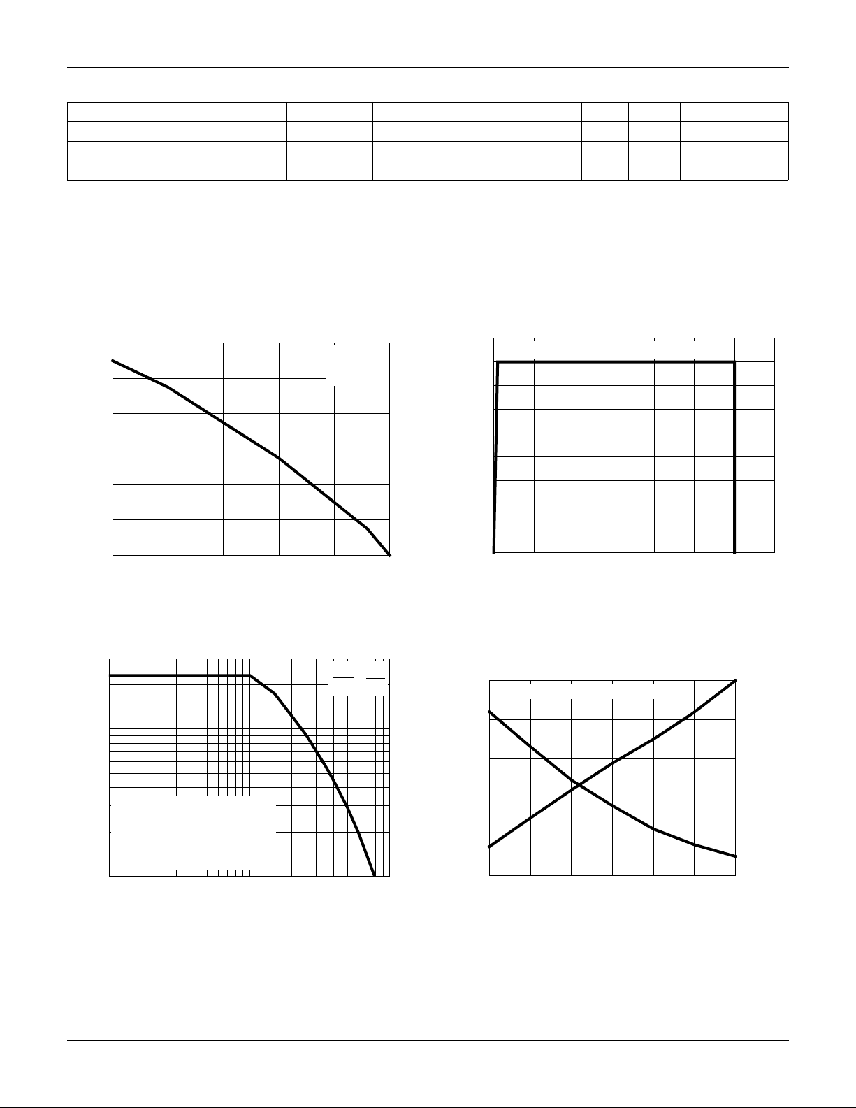
VCE, COLLECTOR TO EMITTER VOLTAGE (V)
700
100
0
I
CE
, COLLECTOR TO EMITTER CURRENT (A)
25
50
300 400200100 500 600
0
125
150
75
175
200
225
TJ = 150oC, RG = 2.2Ω, V
GE
= 15V, L = 100µH
VGE, GATE TO EMITTER VOLTAGE (V)
I
SC
, PEAK SHORT CIRCUIT CURRENT (A)
t
SC
, SHORT CIRCUIT WITHSTAND TIME (ms)
10 11 12 15
2
10
200
1200
t
SC
I
SC
12
1000
13 14
4
6
8
400
600
800
16
VCE = 390V, RG = 2.2Ω, TJ = 125oC
HGT1N40N60A4D
θ
Electrical Specifications T
= 25oC, Unless Otherwise Specified (Continued)
J
PARAMETER SYMBOL TEST CONDITIONS MIN TYP MAX UNITS
Diode Reverse Recovery Time t
Thermal Resistance Junction To Case R
rr
JC
I
= 40A, dI
EC
/dt = 200A/ µ s - 48 55 ns
EC
IGBT - - 0.42
Diode - - 1.8
NOTES:
2. Turn-Off Energy Loss (E
at the point where the collector current equals zero (I
of Power Device Turn-Off Switching Loss. This test method produces the true total Turn-Off Energy Loss.
3. Values for two Turn-On loss conditions are shown for the convenience of the circuit designer. E
turn-on loss when a typical diode is used in the test circuit and the diode is at the same T
) is defined as the integral of the instantaneous power loss starting at the trailing edge of the input pulse and ending
OFF
= 0A). All devices were tested per JEDEC Standard No. 24-1 Method for Measurement
CE
ON1
as the IGBT. The diode type is specified in Figure 20.
J
Typical Performance Curves (Unless Otherwise Specified)
120
100
80
60
40
V
= 15V
GE
TJ = 150oC
is the turn-on loss of the IGBT only. E
ON2
o
C/W
o
C/W
is the
, DC COLLECTOR CURRENT (A)
20
CE
I
0
25 75 100 125 150
50
TC, CASE TEMPERATURE (oC)
FIGURE 1. DC COLLECTOR CURRENT vs CASE
TEMPERATURE
300
100
f
= 0.05 / (t
MAX1
f
= (PD - PC) / (E
MAX2
, OPERATING FREQUENCY (kHz)
MAX
f
FIGURE 3. OPERATING FREQUENCY vs COLLECTOR TO
©2001 Fairchild Semiconductor Corporation HGT1N40N60A4D Rev. B
= CONDUCTION DISSIPATION
P
C
(DUTY FACTOR = 50%)
= 0.42oC/W, SEE NOTES
R
ØJC
10
1 10 20 100
I
EMITTER CURRENT
d(OFF)I
, COLLECTOR TO EMITTER CURRENT (A)
CE
+ t
ON2
+ E
d(ON)I
OFF
FIGURE 2. MINIMUM SWITCHING SAFE OPERATING AREA
V
T
GE
C
15V
75oC
)
)
FIGURE 4. SHORT CIRCUIT WITHSTAND TIME
 Loading...