

Fairchild Semiconductor FDS3590 Datasheet
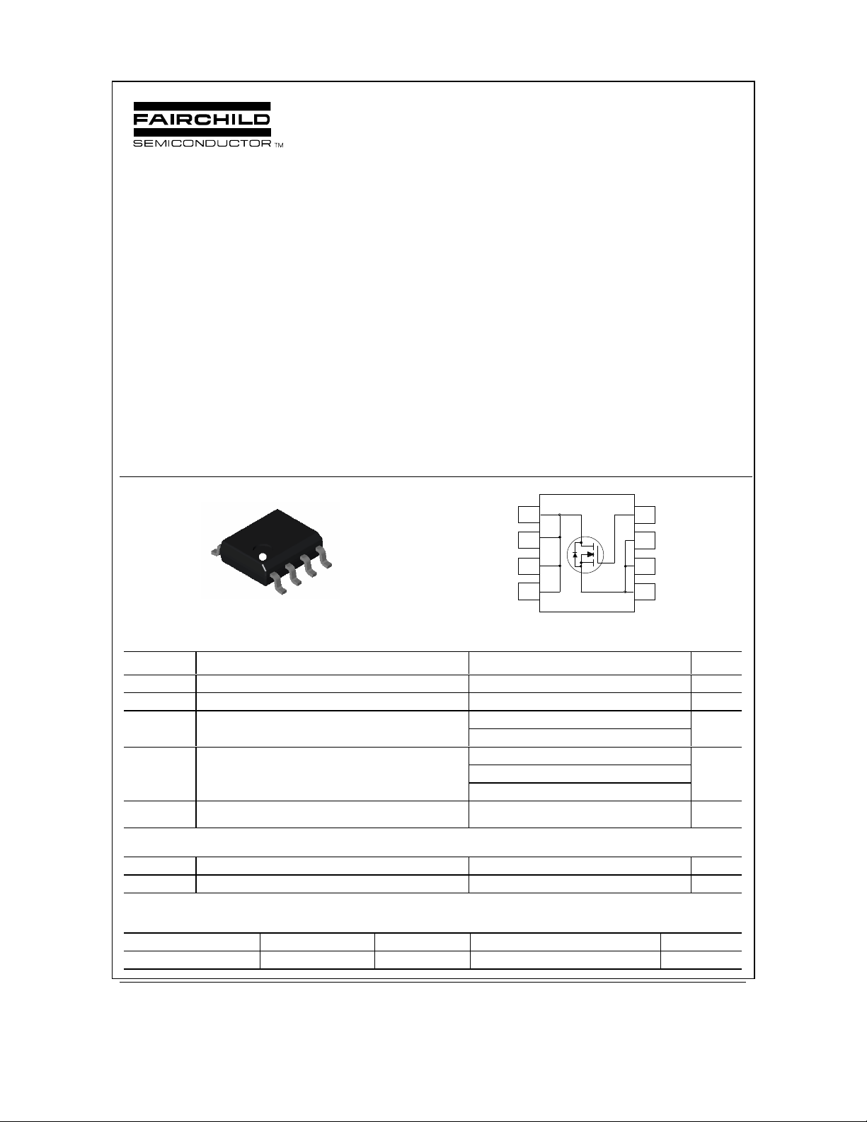
FDS3590
80V N-Channel PowerTrench® MOSFET
FDS3590
January 2000
PRELIMINARY
General Description
This N-Channel MOSFET has been designed
specifically to improve the overall efficiency of DC/ DC
converters using either synchronous or conventional
switching PWM controller s .
Features
6.5 A, 80 V R
•
Low gate charge
•
= 0.037 Ω @ VGS = 10 V
DS(ON)
R
= 0.043 Ω @ VGS = 6 V
DS(ON)
These MOSFETs feature faster switching and lower
gate charge than other MOSFETs with comparable
specifications.
R
DS(ON)
The result is a MOSFET that is easy and safer to drive
(even at very high frequencies), and DC/DC power
supply designs with higher overall efficiency.
D
D
Fast switching speed
•
High performance trench technology for extremely
•
low R
DS(ON)
High power and current handling capability
•
5
4
D
D
G
S
SO-8
S
S
Absolute Maximum Ratings
TA=25oC unless otherwise noted
6
7
8
3
2
1
Symbol Parameter Ratings Units
V
DSS
V
GSS
I
D
P
D
TJ, T
STG
Drain-Source Voltage 80 V
Gate-Source Voltage
Drain Current – Continuous
(Note 1a)
20
±
6.5 A
– Pulsed 50
Power Dissipation for Single Operation
Operating and Storage Junction Temperature
(Note 1a)
(Note 1b)
(Note 1c)
2.5
1.2
1.0
-55 to +150
Range
V
W
°
C
Thermal Characteristics
R
JA
θ
R
JC
θ
Thermal Resistance, Junction-to-Ambient
Thermal Resistance, Junction-to-Case
(Note 1a)
(Note 1)
50
25
Package Marking and Ordering Information
Device Marking Device Reel Size Tape width Quantity
FDS3590 FDS3590 13’’ 12mm 2500 units
1999 Fairchild Semiconductor Corpor ation
C/W
°
C/W
°
FDS3590 Rev B. (W)
FDS3590
Electrical Characteristics
TA = 25°C unless otherwise noted
Symbol Parameter Test Conditions Min Typ Max Units
Off Characteristics
BV
DSS
BV
∆
T
∆
I
DSS
I
GSSF
I
GSSR
On Characteristics
V
GS(th)n
GS(th)
V
∆
T
∆
R
DS(on)
I
D(on)
G
FS
Drain–Source Breakdown Voltage
Breakdown Voltage Temperature
DSS
Coefficient
J
V
= 0 V, ID = 250 µA
GS
I
= 250 µA,Referenced to 25°C
D
80 V
88
Zero Gate Voltage Drain Current VDS = 64 V, VGS = 0 V 1
Gate–Body Leakage, Forward VGS = 20 V, VDS = 0 V 100 nA
Gate–Body Leakage, Reverse VGS = –20 V, VDS = 0 V –100 nA
(Note 2)
Gate Threshold Voltage
Gate Threshold Voltage
Temperature Coefficient
J
Static Drain–Source
On–Resistance
V
= VGS,ID = 250 µA
DS
I
= 250 µA,Referenced to 25°C
D
VGS = 10 V, ID = 6.5 A
= 10 V, ID = 6.5 A, TJ = 125°C
V
GS
= 6 V, ID = 4.5 A
V
GS
24V
–6.0
0.032
0.061
0.034
On–State Drain Current VGS = 10 V, VDS = 5 V 25 A
Forward Transconductance VGS = 10 V, ID = 6.5 A 25 S
0.037
0.086
0.043
mV/°C
A
µ
mV/°C
Ω
Dynamic Characteristics
C
iss
C
oss
C
rss
Switching Characteristics
t
d(on)
t
r
t
d(off)
t
f
Q
g
Q
gs
Q
gd
Input Capacitance 1180 pF
Output Capacitance 171 pF
Reverse Transfer Capacitance
(Note 2)
Turn–On Delay Time 11 20 ns
Turn–On Rise Time 8 16 ns
= 40 V, V
V
DS
f = 1.0 MHz
V
= 40 V, ID = 1 A,
DD
= 10 V, R
V
GS
GS
GEN
= 0 V,
= 6
50 pF
Ω
Turn–Off Delay Time 26 50 ns
Turn–Off Fall Time
Total Gate Charge 25 35 nC
Gate–Source Charge 4.5 nC
V
= 40 V, ID = 6.5 A,
DS
V
= 10 V
GS
Gate–Drain Charge
12 25 ns
5.8 nC
Drain–Source Diode Characteristics and Maximum Ratings
I
S
V
SD
Notes:
R
1.
JA
θ
the drain pins. R
Scale 1 : 1 on letter size paper
Pulse Test: Pulse Width < 300µs, Duty Cycle < 2.0%
2.
Maximum Continuous Drain–Source Diode Forward Current 2.1 A
Drain–Source Diode Forward
VGS = 0 V, IS = 2.1 A
(Note 2)
0.74 1.2 V
Voltage
is the sum of the junction-to-case and case-to-ambient thermal resistance where the case thermal reference is defined as the solder mounting surface of
is guaranteed by design while R
JC
θ
a) 50°/W when
mounted on a 1in
pad of 2 oz copper
is determined by the user's board design.
CA
θ
2
b) 105°/W when
mounted on a 0.04
in2 pad of 2 oz
copper
c) 125°/W when mounted on a
minimum pad.
FDS3590 Rev B. (W)
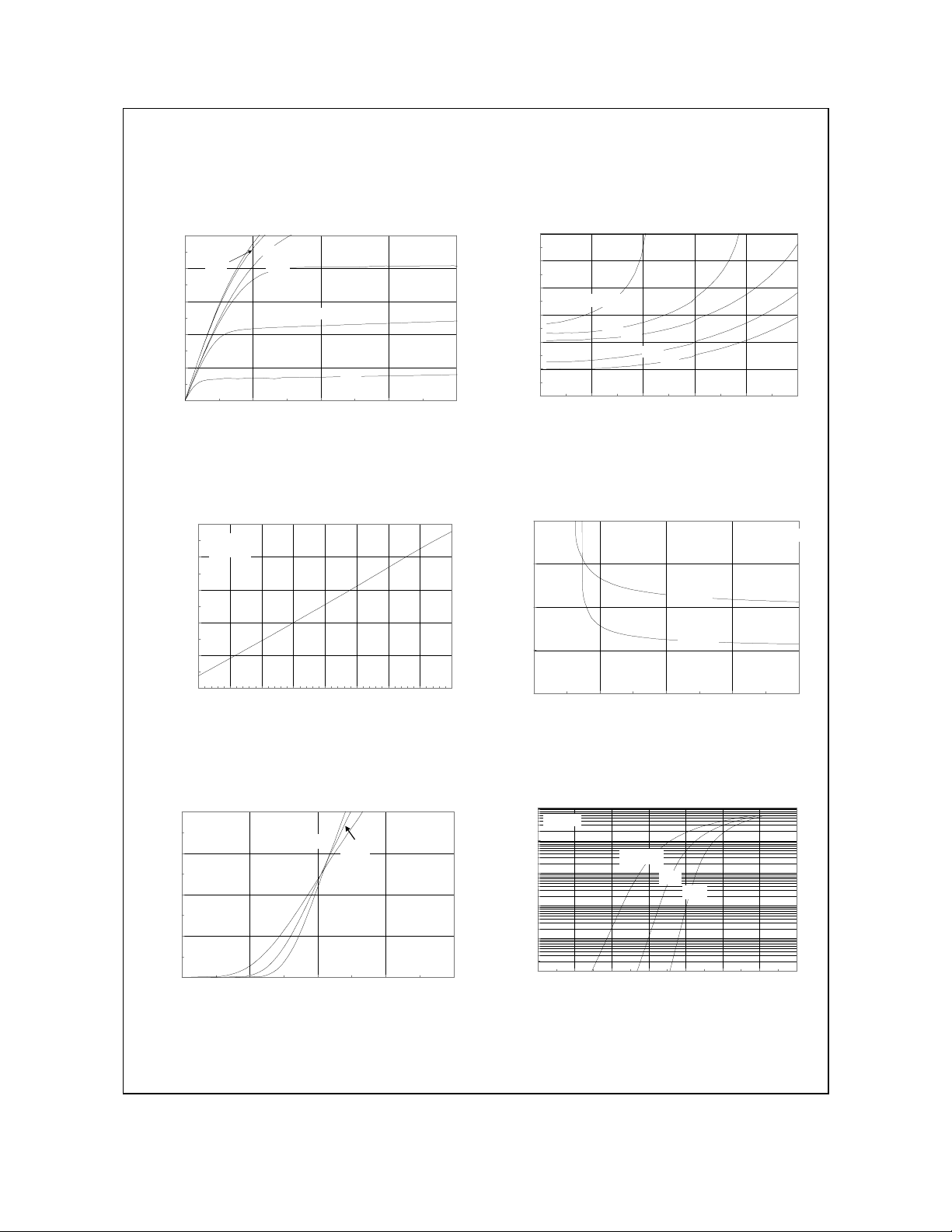
Typical Characteristics
FDS3590
50
VGS = 10V
6.0V
40
30
20
, DRAIN CURRENT (A)
D
I
10
0
02468
5.0V
4.5V
4.0V
3.5V
, DRAIN-SOURCE VOLTAGE (V)
V
DS
2
1.8
1.6
1.4
, NORMALIZED
1.2
DS(ON)
R
1
DRAIN-SOURCE ON-RESISTANCE
0.8
VGS = 4.0V
4.5V
5.0V
6.0V
10V
0 1020304050
, DRAIN CURRENT (A)
I
D
Figure 1. On-Region Characteristics. Figure 2. On-Resistance Variation with
Drain Current and Gate Voltage.
2.2
ID = 6.5A
VGS = 10V
1.8
1.4
, NORMALIZED
1
DS(ON)
R
0.6
DRAIN-SOURCE ON-RESISTANCE
0.2
-50 -25 0 25 50 75 100 125 150
, JUNCTION TEMPERATURE (oC)
T
J
0.1
0.075
T
0.05
, ON-RESISTANCE (OHM)
0.025
DS(ON)
R
0
246810
VGS, GATE TO SOURCE VOLTAGE (V)
= 125oC
TA = 25oC
ID = 3.5 A
Figure 3. On-Resistance Variation with
Temperature.
40
VDS = 5V
30
20
, DRAIN CURRENT (A)
10
D
I
0
23456
TA = -55oC 25oC
, GATE TO SOURCE VOLTAGE (V)
V
GS
125oC
Figure 4. On-Resistance Variation with
Gate-to-Source Voltage.
100
VGS = 0V
10
1
0.1
0.01
, REVERSE DRAIN CURRENT (A)
S
I
0.001
0 0.2 0.4 0.6 0.8 1 1.2 1.4
TA = 125oC
25oC
-55oC
V
, BODY DIODE FORWARD VOLTAGE (V)
SD
Figure 5. Transfer Characteristics. Figure 6. Body Diode Forward Voltage Variation
with Source Current and Temperature.
FDS3590 Rev B. (W)
 Loading...