Fairchild Semiconductor FDR8521L Datasheet

FDR8521L
(
)
y
)
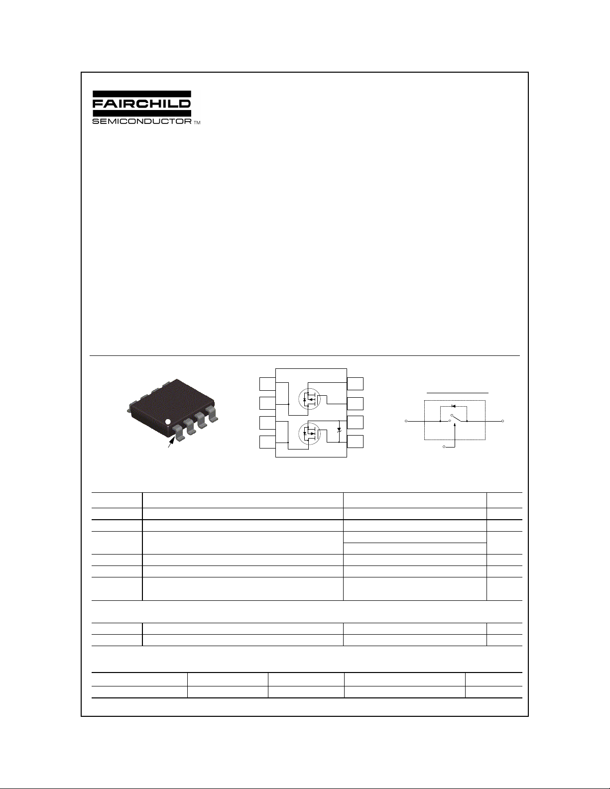
P-Channel MOSFET With Gate Driver For Load Switch Application
FDR8521L
August 2000
General Description
This device is designed for configuration as a load switch
and is particularly suited for power management in portable battery powered electronic equipment. Designed to
operate from 3V to 20V input and supply up to 2.9A, the
device features a small N-Channel MOSFET (Q1) together
with a large P-Channel Power MOSFET (Q2) in a single
SO-8 package.
Applications
• Power management
• Load switch
V
OU T,C1,CO
5
V
OUT ,C1,CO
6
7
2
R
R
2
8
SuperSOT -8
TM
1
pin
Features
• V
= 0.07 V @ VIN= 12 V, IL= 1 A.R
DROP
V
= 0.115 V @ VIN= 5 V, IL= 1 A.R
DROP
• V
= 0.2 V @ VIN= 12 V, IL=2.9 A.R
DROP
V
= 0.2 V @ VIN= 5 V,IL= 1.8 A.R
DROP
(ON)
(ON)
(ON)
(ON)
• Control MOSFET (Q1) includes Zener protection for
ESD ruggedness (>6kV Human Body Model).
• High density cell design for extremely low on-resistance.
VIN,R1,C
i
Q2
Q1
Se e App li cat i o n Ci r c ui t
4
R1,R2,C
1
3
IN
C1,C
O
2
V
ON/OFF
1
EQUIVALENT CIRCUIT
V
DR OP
+
ON/OFF
= 0.07 Ω
= 0.115 Ω.
= 0.07 Ω
= 0.115 Ω.
-
OUT
T
=25oC unless otherwise noted
Absolute Maximum Ratings
A
Symbol Parameter Ratings Units
V
IN
V
ON/OFF
I
D
Input Voltage Range
On/Off Voltage Range 2.5 - 8 V
Load Current - Continuous
- Puls e d 8
P
D
TJ, T
stg
Max im um Powe r D iss ipatio n
Operating and Storage Temperature Range -55 to +150
ESD Electros tatic D isc ha rge Rating MIL-STD-883D
Human-Bod
-Model (100pf/1500 Ohm
(Note 1)
Note 2
(Note 2)
3 - 20 V
2.9 A
0.8 W
6kV
Thermal Characteristics
R
JA
θ
R
JC
θ
Thermal Resistance, Junction-to-Ambient
Thermal Resistance, Junction-to-Case
(Note 2)
(Note 2)
156
40
Package Marking and Ordering Information
Device Marking Device Reel Size Tape width
8521L FDR8521L 13’’ 12mm 3000 units
2000 Fairchild Semiconductor International
C
°
C/W
°
C/W
°
Qua n tity
FDR8521L Rev. C

FDR8521L
Electrical Characteristics
TA=25oC unless otherwise noted
Symbol Parameter Test Conditions Min Typ Max Units
OFF Characteristics
I
FL
ON Characteristics
V
DROP
R
(ON)
I
L
Notes:
1. Range of VIN can be up to 25V, but R1 and R2 must be scaled such that VGS of Q2 does not exceed -20V.
2. R
mounting surface of the drain pins. R
3. Pulse Test: Pulse Width < 300µs, Duty Cycle < 2.0%.
Forward Leakage Current VIN = 20 V, V
(Note 3)
V
Conduction Voltage
IN
V
IN
V
IN
V
IN
= 12 V, V
= 5 V, V
= 12 V, V
= 5 V, V
Q2 - Static On-Resistance VGS = -12 V, ID = 2.9 A
V
= -5 V, ID = 1.8 A
Load Current V
is the sum of the junction-to-case and case-to-ambient thermal resistance where the case thermal reference is defined as the solder
θJA
GS
= 0.2 V, VIN = 12 V, V
DROP
V
= 0.2 V, VIN = 5 V, V
DROP
is guaranteed by design while R
θJC
= 250 µA1
ON/OFF
= 3.3 V, IL = 1 A
ON/OFF
= 3.3 V, IL = 1 A
ON/OFF
= 3.3 V, IL = 2.9 A 0.200
ON/OFF
= 3.3 V, IL = 1.8 A 0.200
ON/OFF
0.053
0.085
0.054
0.090
= 3.3 V
ON/OFF
= 3.3 V
ON/OFF
is determined by the user’s board design.
θJA
2.9
1.8
0.070
0.115
0.070
0.115
µ
V
Ω
A
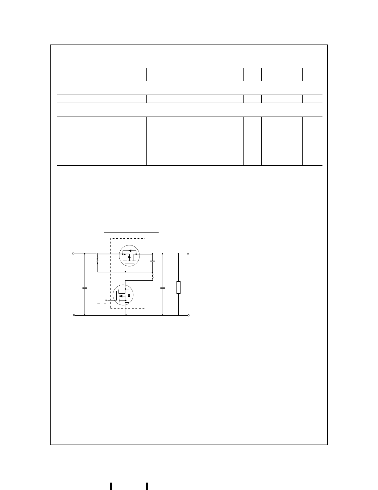
FDR8521L Load Switch Application
APP LICA TI ON CIRCUIT
A
Q2
IN OUT
R1
Ci
ON/OFF
C1
R2
Co
Q1
External Component Recommendation:
For applications where Co ≤ 1µF.
For slew rate control, select R2 in the range of 470 - 10kΩ .
For additional in-rush current control,C1 ≤ 1000pF can be added.
Select R1 so that the R1/R2 ratio ranges from 10 - 100. R1 is required to turn Q2 off.
LOAD
FDR8521L Rev. C

T ypical Characteristics (continued)
µ
FDR8521L
0.7
VIN = 12V
= 1.5 - 8V
V
0.6
ON/OFF
S, D < 2%
PW = 300
0.5
0.4
(V)
DROP
0.3
V
0.2
0.1
0
012345678
TA = 125oC
TA = 25oC
(A)
I
L
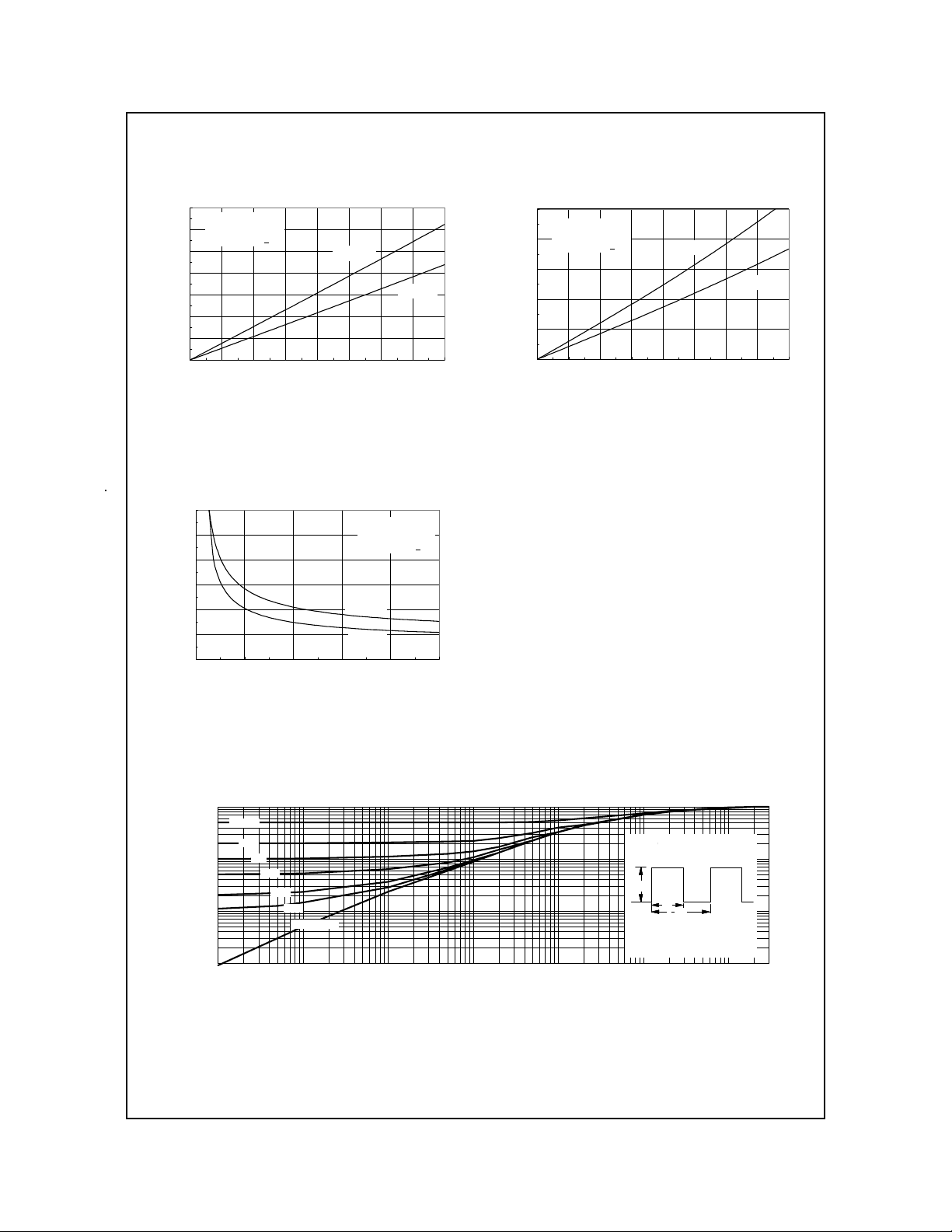
Figure 1. Conduction V oltage Drop
Variation with Load Current.
0.3
0.25
0.2
(V)
0.15
DROP
V
0.1
0.05
0
2 4 6 8 10 12
, INPUT VOLTAGE (V)
V
IN
IL = 1A
V
ON/OFF
PW = 300µS, D <
TA = 125oC
TA = 25oC
= 1.5V -8V
1
VIN = 5V
V
= 1.5 - 8V
ON/OFF
0.8
PW = 300µS, D <
0.6
(V)
DROP
V
0.4
0.2
0
012345678
2%
TA = 125oC
I
(A)
L
TA = 25oC
Figure 2. Conduction V oltage Drop
Variation with Load Current.
2%
Figure 3. On-Resistance V ariation
with Input Volt age.
1
D = 0.5
0.5
R (t) = r(t) * R
JA
0.2
0.2
0.1
0.05
0.02
0.01
0.005
r(t), NORMALIZED EFFECTIVE
0.002
TRANSIENT THERMAL RESISTANCE
0.001
0.1
0.05
0.02
0.01
Single Pulse
0.0001 0.001 0.01 0.1 1 10 100 300
t , TIME (sec)
1
JA
θ
θ
R =
JA
θ
P(pk)
P(pk)
t
t
1
1
t
t
2
2
T - T = P * R (t)
J
J
A
A
Duty Cycle, D = t / t
156
Figure 4.Transient Thermal Response Curve.
Thermal characterization performed using the conditions described in Note 2.
Transient themal response will change depending on the circuit board design.
°C/W
JA
θ
1
JA
θ
2
2
FDR8521L Rev. C
 Loading...