

Fairchild Semiconductor FDR842P Datasheet
December 2001
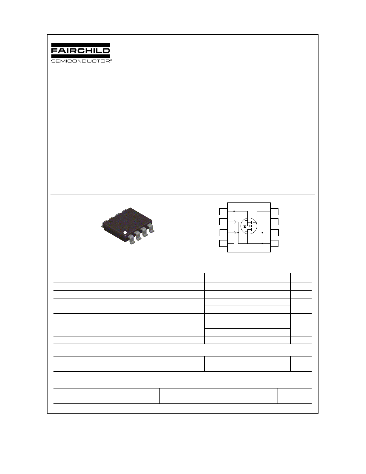
FDR842P
P-Channel 1.8V Specified PowerTrench
MOSFET
FDR842P
General Description
This P-Channel –1.8V specified MOSFET uses
Fairchild’s advanced low voltage PowerTrench process.
It has been optimized for battery power management
applications.
Applications
• Power management
• Load switch
• Battery protection
Features
• –11 A, –12 V R
R
R
• Fast switching speed
• High performance trench technology for extremely
DS(ON)
low R
• High power and current handling capability
= 9 mΩ @ VGS = –4.5 V
DS(ON)
= 12 mΩ @ VGS = –2.5 V
DS(ON)
= 16 mΩ @ VGS = –1.8 V
DS(ON)
S
D
D
S
G
SuperSOT -8
TM
D
D
D
Absolute Maximum Ratings T
o
=25
C unless otherwise noted
A
45
36
27
18
Symbol Parameter Ratings Units
V
Drain-Source Voltage –12 V
DSS
V
Gate-Source Voltage
GSS
ID Drain Current – Continuous (Note 1a) –11 A
– Pulsed –50
PD
TJ, T
STG
Power Dissipation for Single Operation (Note 1a) 1.8
(Note 1b)
Operating and Storage Junction Temperature Range –55 to +150
(Note 1c)
± 8
1.0
0.9
V
W
°C
Thermal Characteristics
R
θJA
R
θJC
Thermal Resistance, Junction-to-Ambient
Thermal Resistance, Junction-to-Case
(Note 1a) 70
(Note 1) 20
Package Marking and Ordering Information
Device Marking Device Reel Size Tape width Quantity
2001 Fairchild Sem iconductor Corporation
FDR842P FDR842P 13’’ 12mm 2500 units
°C/W
°C/W
FDR842P Rev D (W )
FDR842P
Electrical Characteristics T
= 25°C unless otherwise noted
A
Symbol Parameter Test Conditions Min Typ Max Units
Off Characteristics
BV
Drain–Source Breakdown Voltage
DSS
∆BVDSS
∆T
I
Zero Gate Voltage Drain Current VDS = –10 V, VGS = 0 V –1
DSS
I
GSSF
I
GSSR
Breakdown Voltage Temperature
Coefficient
J
Gate–Body Leakage, Forward VGS = 8 V, VDS = 0 V 100 nA
Gate–Body Leakage, Reverse VGS = –8 V, VDS = 0 V –100 nA
= 0 V, ID = –250 µA
V
GS
I
= –250 µA, Referenced to 25°C
D
–12 V
–4.4
mV/°C
µA
On Characteristics (Note 2)
V
Gate Threshold Voltage
GS(th)
∆VGS(th)
∆TJ
R
DS(on)
Gate Threshold Voltage
Temperature Coefficient
Static Drain–Source
On–Resistance
I
On–State Drain Current VGS = –4.5 V, VDS = –5 V –50 A
D(on)
= VGS, ID = –250 µA
V
DS
= –250 µA, Referenced to 25°C
I
D
VGS = –4.5 V, ID = –11 A
= –2.5 V, ID = –9.5 A
V
GS
= –1.8 V, ID = –7.5 A
V
GS
V
= – 4.5 V, ID = –11 A, TJ=125°C
GS
gFS Forward Transconductance VDS = –5 V, ID = –11 A 56 S
–0.4 –0.5 –1.5 V
2.7
7
9
12
9
9
12
16
12
mV/°C
mΩ
Dynamic Characteristics
C
Input Capacitance 5350 pF
iss
C
Output Capacitance 2135 pF
oss
C
Reverse Transfer Capacitance
rss
= –6 V, V
V
DS
f = 1.0 MHz
= 0 V,
GS
1386 pF
Switching Characteristics (Note 2)
t
Turn–On Delay Time 17 30 ns
d(on)
tr Turn–On Rise Time 20 35 ns
t
Turn–Off Delay Time 201 322 ns
d(off)
tf Turn–Off Fall Time
Qg Total Gate Charge 57 80 nC
Qgs Gate–Source Charge 7 nC
Qgd Gate–Drain Charge
= –6 V, ID = –1 A,
V
DD
= –4.5 V, R
V
GS
= –6 V, ID = –11 A,
V
DS
V
= –4.5 V
GS
GEN
= 6 Ω
161 258 ns
16 nC
Drain–Source Diode Characteristics and Maximum Ratings
IS Maximum Continuous Drain–Source Diode Forward Current –1.5 A
VSD
Notes:
1. R
is the sum of the junction-to-case and case-to-ambient thermal resistance where the case thermal reference is defined as the solder mounting surface of
θJA
the drain pins. R
Scale 1 : 1 on letter size paper
2. Pulse Test: Pulse Width < 300µs, Duty Cycle < 2.0%
Drain–Source Diode Forward
Voltage
is guaranteed by design while R
θJC
a) 70°/W when
mounted on a 1in2
pad of 2 oz copper
θCA
VGS = 0 V, IS = –1.5 A (Note 2) –0.6 –1.2 V
is determined by the user's board design.
b) 125°/W when
mounted on a .04 in
pad of 2 oz copper
2
c) 135°/W when mounted on a
mini mum pa d.
FDR842P Rev D (W )
 Loading...