

Fairchild Semiconductor FDR836P Datasheet

FDR836P
P-Channel 2.5V Specified MOSFET
FDR836P
April 1999
General Description
SuperSOT
field effect transistors are produced using Fairchild’s
proprietary, high cell density, DMOS technology. This
very high density process is especially tailored to minimize on-state resistance and provide superior switching performance. These devices are particularly suited
for low voltage applications such as battery powered
circuits or portable electronics where low in-line power
loss, fast switching and resistance to transients are
needed.
Absolute Maximum Ratings
TM
-8 P-Channel enhancement mode power
S
D
D
S
G
SuperSOT -8
TM
D
D
D
TA = 25°C unless otherwise noted
Features
• -6.1 A, -20 V. R
R
• High density cell design for extremely low R
= 0.030 W @ VGS = -4.5 V
DS(ON)
= 0.040 W @ VGS = -2.5 V
ON)
DS(
DS(ON)
.
• Small footprint (38% smaller than a standard SO-8); low
profile package (1 mm thick); power handling capability
similar to SO-8.
5
6
7
8
4
3
2
1
Symbol Parameter Ratings Units
V
DSS
V
GSS
I
D
P
D
TJ, T
stg
Drain-Source Voltage -20 V
Gate-Source Voltage
Drain Current - Continuous
(Note 1a)
8V
±
-6.1 A
- Pulsed -18
Power Dissipation for Single Operation
(Note 1a)
(Note 1b)
(Note 1c)
1.8 W
1.0
0.9
Operating and Storage Junction Temperature Range -55 to +150
Thermal Characteristics
R
JA
θ
R
JC
θ
Thermal Resistance, Junction-t o-Amb i ent
Thermal Resistance, Junction-t o-Case
(Note 1a)
(Note 1)
70
20
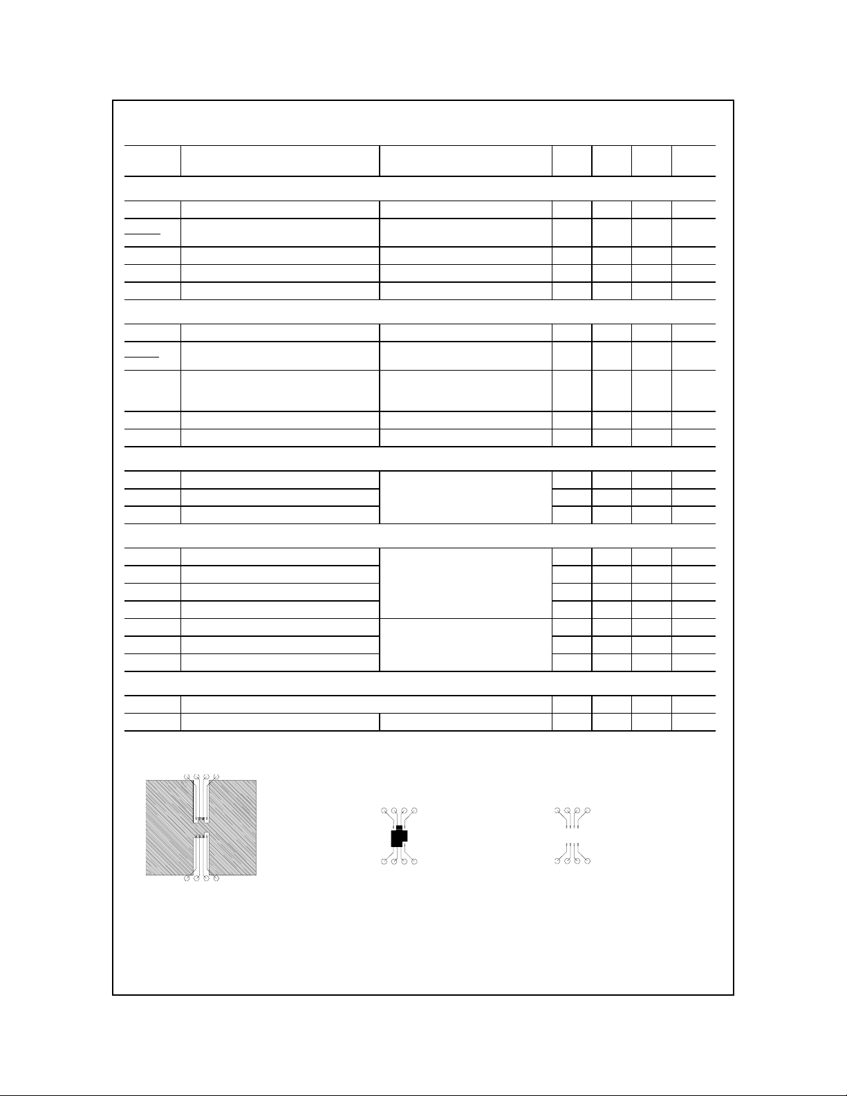
Package Outlines and Ordering Information
Device Marking Device Reel Size Tape Width Quantity
836P
.
ã1999 Fairchild Semiconductor Corporation
FDR836P 13’’ 12mm 3000 units
C
°
C/W
°
C/W
°
FDR836P, Rev. C
FDR836P
yp
)
Electrical Characteristics
TA = 25°C unless otherwise noted
Symbol Parameter Test Conditions Min T
Off Characteristics
BV
DSS
BV
∆
T
∆
I
DSS
I
GSSF
I
GSSR
On Characteristics
V
GS(th)
GS(th)
V
∆
T
∆
R
DS(on)
I
D(on)
g
FS
Drain-Source Breakdown Voltage VGS = 0 V, ID = -250 µA-20 V
DSS
Breakdown Voltage Temperature
Coefficient
J
ID= -250 µA, Referenced to 25°C-24mV/
Zero Gate Voltage Drain Current VDS = -16 V, VGS = 0 V -1
Gate-Body Leakage Current, Forward VGS = 8 V, VDS = 0 V 100 nA
Gate-Body Leakage Current, Reverse VGS = -8 V, VDS = 0 V -100 nA
(Note 2)
Gate Threshold Voltage VDS = VGS, ID = -250 µA-0.4-0.6-1V
Gate Threshold Voltage
Temperature Coefficient
J
Static Drain-Source
On-Resistance
ID = -250 µA, Referenced to 25°C3mV/
VGS = -4.5 V, ID = -6.1 A
V
= -4.5V, ID =-6.1 A,TJ=125°C
GS
V
= -2.5 V, ID = -5 A
GS
On-State Drain Current VGS = -4.5 V, VDS = -5 V -9 A
Forward Transconductance VDS = -5 V, ID = -6.1A 22 S
Dynamic Characteristics
C
iss
C
oss
C
rss
Input Capacitance 2200 pF
Output Capacitance 570 pF
= -25 V, VGS = 0 V,
V
DS
f = 1.0 MHz
Reverse Transfer Capacitance
Max Units
0.030
0.022
0.048
0.031
0.040
0.029
140 pF
C
°
A
µ
C
°
Ω
(Note 2)
Switching Characteristics
t
d(on)
t
r
t
d(off)
t
f
Q
Q
Q
g
gs
gd
Turn-On Delay Time 10 18 ns
Turn-On Rise Time 14 25 ns
Turn-Off Delay Time 225 360 ns
Turn-Off Fall Time
Total Gate Charge 32 44 nC
Gate-Source Charge 3.2 nC
Gate-Drain Charge
V
= -10 V, ID = -1 A,
DD
V
= -4.5 V, R
GS
= -10 V, ID = -6.1 A,
V
DS
V
= - 4.5 V
GS
GEN
= 6
Drain-Source Diode Characteristics and Maximum Ratings
I
S
V
SD
Notes:
1. R
surface of the drain Pins. R
Maximum Continuous Drain-Source Diode Forward Current -1.5 A
Drain-Source Diode Forward Voltage V
is the sum of the junction-to-case and case-to-ambient thermal resistance where the case thermal reference is defined as the solder mounting
qJA
is guaranteed by design while R
qJC
a) 70°C/W when mounted on a
1.0 in2 pad of 2 oz. copper.
qCA
= 0 V, I
is determined by the user's board design.
= -1.5 A
b) 125°C/W when mounted on a
0.026 in2 pad of 2oz. copper.
Scale 1 : 1 on letter size paper
2. Pulse Test: Pulse Width £ 300 ms, Duty Cycle £ 2.0%
Ω
(Note 2
85 135 ns
8.1 nC
-0.65 -1.2 V
c) 135°C/W when mounted on a
minimum pad.
FDR836P, Rev. C

T ypical Characteristics
FDR836P
20
VGS = -4.5V
16
-3.0V
12
8
4
, DRAIN-SOURCE CURRENT (A)
D
-I
0
00.511.522.53
-2.5V
-
-1.5V
, DRAIN-SOURCE VOLTAGE (V)
-V
DS
Figure 1. On-Region Characteristics.
1.6
ID = -6.1A
= -4.5V
V
GS
1.4
1.2
, NORMALIZED
1
DS(ON)
R
0.8
DRAIN-SOURCE ON-RESISTANCE
0.6
-50 -25 0 25 50 75 100 125 150
, JUNCTION TEMPERATURE (oC)
T
J
2
1.8
1.6
VGS = -2.0V
1.4
, NORMALIZED
1.2
DS(ON)
R
1
DRAIN-SOURCE ON-RESISTANCE
0.8
048121620
-2.5V
-3.0V
, DIRAIN CURRENT (A)
-I
D
-3.5V
-4.0V
-4.5V
Figure 2. On-Resistance Variation
with Drain Current and Gate V oltage.
0.1
0.08
0.06
0.04
, ON-RESISTANCE (OHM)
0.02
DS(ON)
R
0
12345
, GATE TO SOURCE VOLTAGE (V)
-V
GS
TA = 125oC
TA = 25oC
ID = -3 A
Figure 3. On-Resistance Variation
with Temperature.
20
VDS = -5V
16
12
8
, DRAIN CURRENT (A)
D
-I
4
0
00.511.522.5
-V
, GATE TO SOURCE VOLTAGE (V)
GS
TA = -55oC
25oC
125oC
Figure 4. On-Resistance Variation
with Gate-to-Source Voltage.
100
VGS = 0V
10
1
TA = 125oC
0 0.2 0.4 0.6 0.8 1 1.2
-V
SD,
25oC
-55oC
BODY DIODE FORWARD VOLTAGE (V)
, REVERSE DRAIN CURRENT (A)
S
-I
0.1
0.01
0.001
0.0001
Figure 5. Transfer Characteristics. Figure 6. Body Diode Forward V oltage
Variation with Source Current
and Temperature.
FDR836P, Rev. C
 Loading...