

Fairchild Semiconductor FDR4420A Datasheet
June 1998
FDR4420A
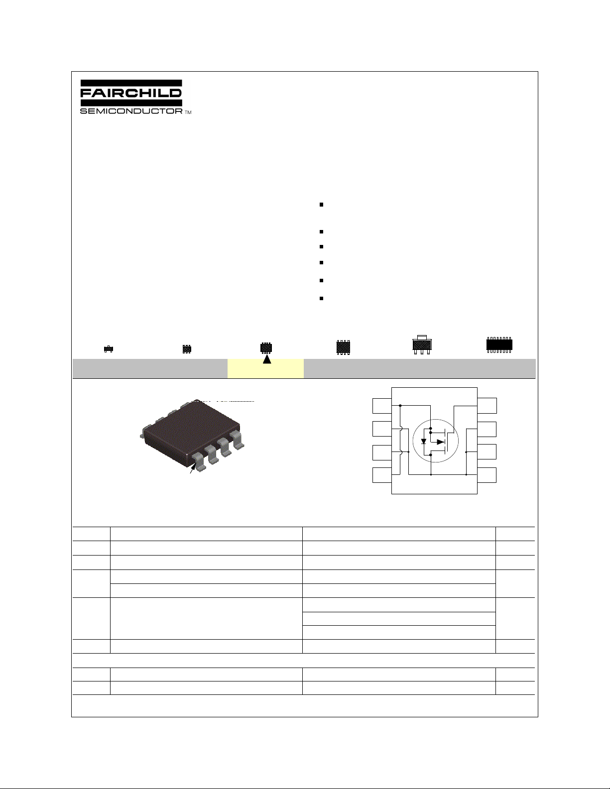
Single N-Channel, Logic Level, PowerTrenchTM MOSFET
General Description Features
The SuperSOT-8 family of N-Channel Logic Level MOSFETs
have been designed to provide a low profile, small footprint
alternative to industry standard SO-8 little foot type product.
These MOSFETs are produced using Fairchild Semiconductor's
advanced PowerTrench process that has been tailored to
minimize the on-state resistance and yet maintain superior
switching performance.
These devices are well suited for low voltage and battery
powered applications where small package size is required
without compromising power handling and fast switching.
SOT-23
SuperSOTTM-6
S
SuperSOTTM-8
D
D
S
4420A
G
D
D
1
pin
SuperSOT -8
TM
D
11 A, 30 V. R
R
= 0.009 Ω @ VGS = 10 V,
DS(ON)
= 0.013 Ω @ VGS = 4.5 V.
DS(ON)
Fast switching speed.
Low gate charge.
Small footprint 38% smaller than a standard SO-8.
Low profile package(1mm thick).
Power handling capability similar to SO-8.
SO-8
SOT-223
5
6
7
8
SOIC-16
4
3
2
1
Absolute Maximum Ratings T
= 25oC unless otherwise noted
A
Symbol Parameter FDR4420A Units
V
DSS
V
GSS
I
D
Drain-Source Voltage 30 V
Gate-Source Voltage ±20 V
Draint Current - Continuous (Note 1a) 11 A
- Pulsed 40
P
D
TJ,T
Maximum Power Dissipation (Note 1a) 1.8
(Note 1b)
(Note 1c)
Operating and Storage Temperature Range -55 to 150 °C
STG
1
0.9
W
THERMAL CHARACTERISTICS
R
θJA
R
θJC
© 1998 Fairchild Semiconductor Corporation
Thermal Resistance, Junction-to-Ambient (Note 1a) 70 °C/W
Thermal Resistance, Junction-to-Case (Note 1) 20 °C/W
FDR4420 Rev.D
Electrical Characteristics (T
= 25OC unless otherwise noted )
A
Symbol Parameter Conditions Min Typ Max Units
OFF CHARACTERISTICS
BV
∆BV
I
DSS
I
GSS
I
GSS
DSS
DSS
Drain-Source Breakdown Voltage VGS = 0 V, ID = 250 µA 30 V
Breakdown Voltage Temp. Coefficient
/∆T
J
Zero Gate Voltage Drain Current
ID = 250 µA, Referenced to 25 o C
VDS = 24 V, V
GS
Gate - Body Leakage Current VGS = 20 V, VDS= 0 V 100 nA
Gate - Body Leakage, Reverse
VGS = -20 V, VDS= 0 V
ON CHARACTERISTICS (Note 2)
∆V
V
R
GS(th)
GS(th)
DS(ON)
Gate Threshold Voltage Temp.Coefficient ID = 250 µA, Referenced to 25 o C -6 mV /oC
/∆T
J
Gate Threshold Voltage VDS = VGS, ID = 250 µA 1 1.4 3 V
Static Drain-Source On-Resistance
VGS = 10 V, ID = 11A
VGS = 4.5 V, ID = 9 A
I
g
D(ON)
FS
On-State Drain Current VGS = 10 V, VDS = 5 V 30 A
Forward Transconductance
VDS = 10 V, ID= 11 A
DYNAMIC CHARACTERISTICS
C
iss
C
oss
C
rss
Input Capacitance VDS = 15 V, VGS = 0 V,
Output Capacitance 560 pF
f = 1.0 MHz
Reverse Transfer Capacitance 280 pF
SWITCHING CHARACTERISTICS (Note 2)
t
t
t
t
Q
Q
Q
D(on)
r
D(off)
f
g
gs
gd
Turn - On Delay Time
Turn - On Rise Time 15 27 ns
VDD = 10 V, ID = 1 A,
VGS = 10V, R
GEN
Turn - Off Delay Time 25 40 ns
Turn - Off Fall Time 21 34 ns
Total Gate Charge
Gate-Source Charge 7 nC
VDS = 15 V, ID = 9.3 A,
VGS = 5 V
Gate-Drain Charge 11 nC
DRAIN-SOURCE DIODE CHARACTERISTICS AND MAXIMUM RATINGS
= 0 V
= 1 Ω
20
1 µA
TJ = 55°C
10 µA
-100 nA
0.0075 0.009
TJ =125°C 0.0125 0.016
0.01 0.013
25 S
2560 pF
11 20 ns
23 33 nC
mV /oC
Ω
I
S
V
SD
Notes:
1. R
is the sum of the junction-to-case and case-to-ambient thermal resistance where the case thermal reference is defined as the solder mounting surface of the drain pins. R
JA
θ
while R
Scale 1 : 1 on letter size paper
2. Pulse Test: Pulse Width < 300µs, Duty Cycle < 2.0%.
Maximum Continuous Drain-Source Diode Forward Current 1.5 A
Drain-Source Diode Forward Voltage
is determined by the user's board design. R
CA
θ
a. 70OC/W on a 1 in2 pad of 2oz
copper.
shown below for single device operation on FR-4 board in still air.
JA
θ
VGS = 0 V, IS = 1.5 A (Note 2)
b. 125OC/W on a 0.026 in2 of pad
of 2oz copper.
c. 135OC/W on a 0.005 in2 of pad
of 2oz copper.
0.7 1.2 V
is guaranteed by design
JC
θ
FDR4420 Rev.D
 Loading...