

Fairchild Semiconductor FDP8030L Datasheet
November 1999
1999 Fairchild Semiconductor Corporation
FDP8030L Rev C(W)
FDP8030L/FDB8030L
N-Channel Logic Level PowerTrench MOSFET
General Description
This N-Channel Logic level MOSFET has been
designed specifically to improve the overall effici ency of
DC/DC converters using either synchronous or
conventional switching PWM controllers.
These MOSFETS feature faster switching and lower
gate charge than other MOSFETS with comparable
R
DS(on)
specifications.
The result is a MOSFET that is easy and safer to drive
(even at very high frequencies), and DC/DC power
supply designs with higher overall efficiency.
Features
•
80 A, 30 V. R
DS(ON)
= 0.0035 Ω @ VGS = 10 V
R
DS(ON)
= 0.0045 Ω @ VGS = 4.5 V
•
Critical DC electrical parameters specified at
elevated temperature
•
Rugged internal source-drain diode can eliminate the
need for an external Zener diode transient
suppressor
•
High performance trench technology for extremely
low R
DS(ON)
•
175°C maximum junction temperature rating
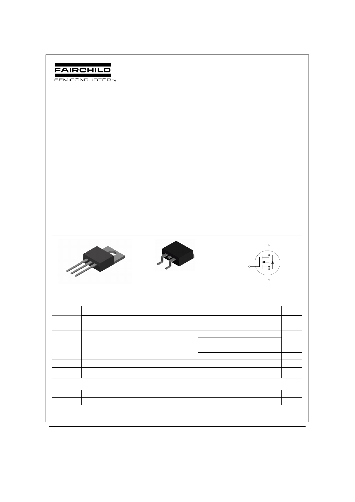
S
G
D
TO-220
FDP Series
D
G
S
TO-263AB
FDB Series
S
D
G
Absolute Maximum Ratings
TA=25oC unless otherwise noted
Symbol Parameter Ratings Units
V
DSS
Drain-Source Voltage 30 V
V
GSS
Gate-Source Voltage
±
20
V
I
D
Drain Current – Continuous
(Note 1)
80 A
– Pulsed
(Note 1)
300
P
D
Total Power Dissipation @# TC = 25°C
187 W
Derate above 25°C
1.25
W°C
TJ, T
STG
Operating and Storage Junction Temperature Range -65 to +175
°
C
T
L
Maximum lead temperature for soldering purposes,
1/8” from case for 5 seconds
275
°
C
Thermal Characteristics
R
θ
JC
Thermal Resistance, Junction-to-Case 0.8
°
C/W
R
θ
JA
Thermal Resistance, Junction-to-Ambient 62.5
°
C/W
FDP8030L/FDB8030L
FDP8030L Rev C(W)
Electrical Characteristics
TA = 25°C unless otherwise noted
Symbol Parameter Test Conditions Min Typ Max Units
Drain-Source Avalanche Ratings
(Note 1)
W
DSS
Single Pulse Drain-Source
Avalanche Energy
VDD = 20 V, ID = 80 A 1500 mJ
I
AR
Maximum Drain-Source Avalanche
Current
80 A
Off Characteristics
BV
DSS
Drain–Source Breakdown Voltage
V
GS
= 0 V, ID = 250 µA
30 V
∆
BV
DSS
∆
T
J
Breakdown Voltage Temperature
Coefficient
I
D
= 250 µA, Referenced to 25°C
23
mV/°C
I
DSS
Zero Gate Voltage Drain Current
V
DS
= 24 V, VGS = 0 V 10
µ
A
I
GSSF
Gate–Body Leakage, Forward
V
GS
= 20 V, VDS = 0 V 100 nA
I
GSSR
Gate–Body Leakage, Reverse
V
GS
= –20 V VDS = 0 V –100 nA
On Characteristics
(Note 2)
V
GS(th)
Gate Threshold Voltage
V
DS
= VGS, ID = 250 µA
11.52 V
∆
V
GS(th)
∆
T
J
Gate Threshold Voltage
Temperature Coefficient
I
D
= 250 µA, Referenced to 25°C
–5
mV/°C
VGS = 10 V, ID = 80 A
T
J
=125°C
3.1
4.0
3.5
5.6
m
Ω
R
DS(on)
Static Drain–Source
On–Resistance
V
GS
= 4.5 V, ID = 70 A 3.6 4.5
I
D(on)
On–State Drain Current
V
GS
= 10 V, VDS = 10 V 60 A
g
FS
Forward Transconductance
V
DS
= 10 V, ID = 80 A 170 S
Dynamic Characteristics
C
iss
Input Capacitance
10500 pF
C
oss
Output Capacitance
2700 pF
C
rss
Reverse Transfer Capacitance
V
DS
= 15 V, V
GS
= 0 V,
f = 1.0 MHz
1650 pF
Switching Characteristics
(Note 2)
t
D(on)
Turn–On Delay Time 20 35 ns
t
r
Turn–On Rise Time 185 225 ns
t
D (off)
Turn–Off Delay Time 160 200 ns
t
f
Turn–Off Fall Time
V
DD
= 15 V, ID = 50 A,
V
GS
= 4.5 V, R
GEN
= 10
Ω
R
GS
= 10
Ω
200 240 ns
Q
g
Total Gate Charge 120 170 nC
Q
gs
Gate–Source Charge 27 nC
Q
gd
Gate–Drain Charge
V
DS
= 15 V,
I
D
= 80 A, VGS = 5 V
48 nC
Drain–Source Diode Characteristics and Maximum Ratings
I
S
Maximum Continuous Drain–Source Diode Forward Current
(Note 1)
80 A
I
SM
Maximum Pulsed Drain-Source Diode Forward Current
(Note 1)
300 A
V
SD
Drain–Source Diode Forward Voltage VGS = 0 V, IS = 80 A
(Note 1)
11.3 V
Notes:
1.
Pulse Test: Pulse Width < 300µs, Duty Cycle < 2.0%
FDP8030L Rev C(W)
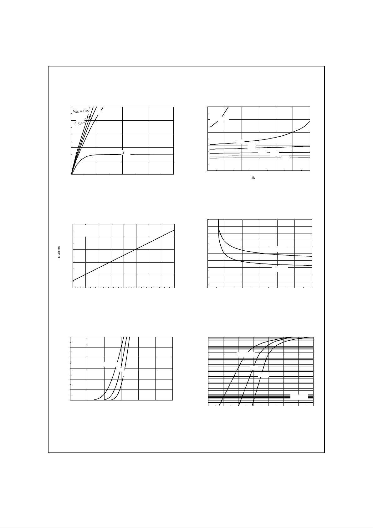
Typical Characteristics
0 0.5 1 1.5 2
0
20
40
60
80
100
V , DRAIN-SOURCE VOLTAGE (V)
I , DRAIN-SOURCE CURRENT (A)
3.5V
2.5V
4.5V
DS
D
3.0V
0 20406080100120
0.5
1
1.5
2
2.5
3
I , DRAIN CURRENT (A)
DRAIN-SOURCE ON-RESISTANCE
V = 2.5V
GS
10V
3.5V
4.5V
D
6.0V
3.0V
R , NORMALIZED
DS(ON)
Figure 1. On-Region Characteristics. Figure 2. On-Resistance Variation with
Drain Current and Gate Voltage.
-50 -25 0 25 50 75 100 125 150
0.6
0.8
1
1.2
1.4
1.6
T , JUNCTION TEMPERATURE (°C)
DRAIN-SOURCE ON-RESISTANCE
J
R , NORMALIZED
DS(ON)
V = 10V
GS
I = 80A
D
0
0.001
0.002
0.003
0.004
0.005
0.006
0.007
0.008
0.009
0.01
2345678
V
GS
, GATE TO SOURCE VOLT AGE ( V )
R
DS(ON)
, ON-RESISTANCE (OHM)
ID = 40A
TA = 125oC
TA = 25oC
Figure 3. On-Resistance Variation with
Temperature.
Figure 4. On-Resistance Variation with
Gate-to-Source Voltage.
1234
0
10
20
30
40
50
60
V , GATE T O SOURCE VOLT AGE (V)
I , DRAIN CURRENT (A)
GS
25°C
125°C
V = 10V
DS
D
T = -55°C
A
0 0.2 0.4 0.6 0.8 1 1.2 1.4
0.0001
0.001
0.01
0.1
1
10
60
V , BODY DIODE FORWARD VOLTAGE (V)
I , REVERSE DRAIN CURRENT (A)
T = 125°C
A
25°C
-55°C
V = 0V
GS
SD
S
Figure 5. Transfer Characteristics. Figure 6. Body Diode Forward Voltage Variation
with Source Current and Temperature.
FDP8030L/FDB8030L
 Loading...