Fairchild Semiconductor FAN1084 Datasheet

www.fairchildsemi.com
FAN1084
4.5A Adjustable/Fixed Low Dropout Linear Regulator
Features
• Fast transient response
• Low dropout voltage at up to 4.5A
• Load regulation: 0.5% typical
• On-chip thermal limiting
• Standard TO-220, TO-263 center cut, and TO-252
packages
Applications
• Desktop PCs, RISC and embedded processors’ supply
• GTL, SSTL logic Reference bus supply
• Low voltage VCC logic supply
• Battery-powered circuitry
• Post regulator for switching supply
• Cable and ADSL modems’ DSP core supply
• Set Top Boxes and Web Boxes modules’ supply
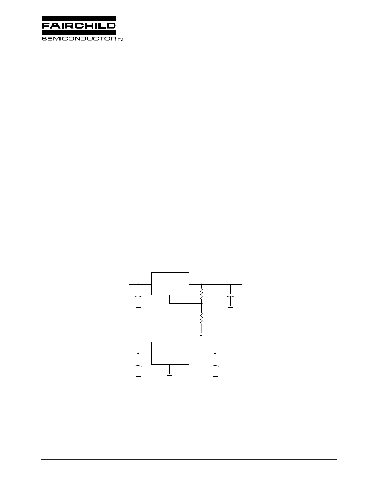
Application Diagrams
FAN1084
= 5V
V
IN
10µF
V
IN
+
ADJ
V
Description
The FAN1084, FAN1084-1.5, and FAN1084-3.3 are low
dropout three-terminal regulators with 4.5A output current
capability. These devices have been optimized for low voltage
applications including V
response and minimum input voltage are critical. The
FAN1084 is ideal for low voltage microprocessor applications requiring a regulated output from 1.5V to 3.6A with an
input supply of 5V or less. The FAN1084-1.5 offers fixed
1.5V with 4.5A current capabilities for GTL+ bus V
termination. The FAN1084-3.3 offers a fixed 3.3V output
at 4.5A.
On-chip thermal limiting provides protection against any
combination of overload and ambient temperature that
would create excessive junction temperatures.
The FAN1084 series regulators are available in the industrystandard TO-220, TO-263 center cut, and TO-252 (DPAK)
power packages.
OUT
124Ω
+
22µF
bus termination, where transient
TT
2.5V at 4.5A
TT
V
= 3.3V
IN
10µF
+
FAN1084-1.5
V
IN
GND
V
OUT
124Ω
+
22µF
1.5V at 4.5A
REV. 1.0.6 11/18/02

FAN1084 PRODUCT SPECIFICATION
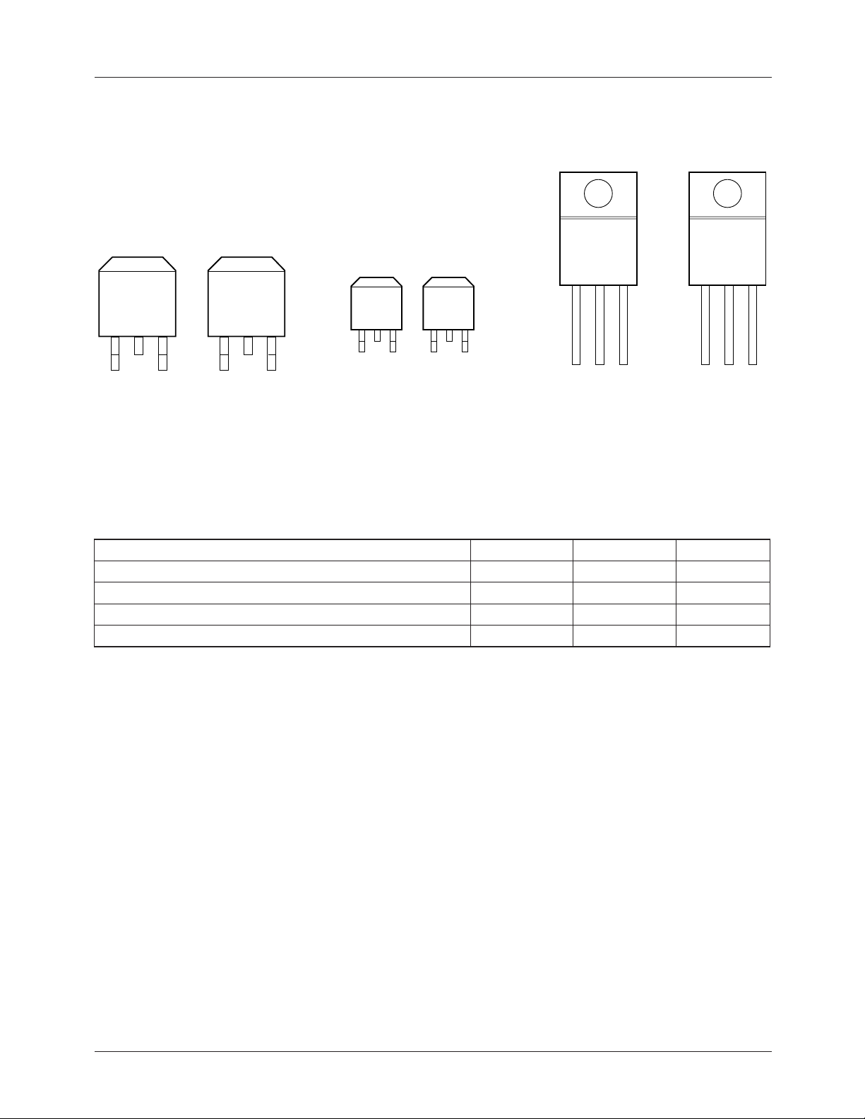
Pin Assignments
FAN1084T
FRONT VIEW
FAN1084M-3.3
FAN1084M-1.5
FRONT VIEW
12 3
GND
*With package soldered to 0.5 square inch copper area over backside ground plane or internal power plane, Θ
30°C/W to more than 40°C/W. Other mounting techniques may provide better power dissipation than 30°C/W.
†
FAN1084M-3.3 also available with uncut center lead.
†
FAN1084M
FRONT VIEW
12 3
IN
3-Lead Plastic TO-263
Θ
JC
ADJ
=3°C/W*
IN
Tab is out.
FAN1084D-3.3
FAN1084D-1.5
FRONT VIEW
123
GND
3-Lead Plastic TO-252
FRONT VIEW
IN
ΘJC=3°C/W*
FAN1084D
123
ADJ
IN
Tab is out.
12 3
ADJ OUT
Absolute Maximum Ratings
IN
3-Lead Plastic TO-220
Θ
=3°C/W*
JC
can vary from
JA
FAN1084T-3.3
FAN1084T-1.5
FRONT VIEW
12 3
GND OUT
IN
Parameter Min. Max. Unit
V
IN
7V
Operating Junction Temperature Range 0 125 °C
Storage Temperature Range –65 150 °C
Lead Temperature (Soldering, 10 seconds) 300 °C
2 REV. 1.0.6 11/18/02

PRODUCT SPECIFICATION FAN1084
Electrical Characteristics
Operating Conditions: 4.75 ≤ VIN < 5.25V, Tj = 25°C unless otherwise specified.
Parameter Conditions Min. Typ. Max Units
Reference Voltage
Output Voltage
Output Voltage
Line Regulation
Load Regulation
5
6
1, 2
1, 2
3
Adj connected to ground, I
I
= 10mA 1.475 1.5 1.525 V
OUT
I
= 10mA 3.234 3.3 3.366 V
OUT
I
= 10mA 0.5 2 %
OUT
10mA ≤ I
≤ 4.5A 0.5 2.5 %
OUT
= 10mA 1.23 1.250 1.27 V
OUT
Dropout Voltage ∆V
Current Limit (V
Adjust Pin Current
Mimimum Load Current
Quiescent Current
Thermal Resistance,
Junction to Case
Thermal Shutdown
Notes:
1. See thermal regulation specifications for changes in output voltage due to heating effects. Load and line regulation are
measured at a constant junction temperature by low duty cycle pulse testing.
2. Line and load regulation are guaranteed up to the maximum power dissipation. Power dissipation is determined by input/
output differential and the output currrent. Guaranteed maximum output power will not be available over the full input/output
voltage range.
3. FAN1084 only.
4. Guaranteed by design.
5. FAN1084-1.5 only.
6. FAN1084-3.3 only.
3
4
1.5V ≤ (VIN – V
4
VIN = 5V 4 mA
TO-220 3 °C/W
TO-263 Center Cut, TO-252 3 °C/W
4
REF%
– V
IN
= 2%, I
) = 2V 5.5 A
OUT
= 4.5A 1.5 V
OUT
35 100 µΑ
) ≤ 5.75V 10 mA
OUT
150 °C
Typical Performance Characteristics
20
15
10
5
POWER (W)
0
25 45 65 85 105 125
CASE TEMPERATURE
Figure 1. Maximum Power Dissipation
REV. 1.0.6 11/18/02 3

FAN1084 PRODUCT SPECIFICATION
Applications Information
General
The FAN1084, FAN1084-1.5, and FAN1084-3.3 are threeterminal regulators optimized for GTL+ VTT termination
and logic applications. These devices are short-circuit protected, and offer thermal shutdown to turn off the regulator
when the junction temperature exceeds about 150°C. The
FAN1084 series provides low dropout voltage and fast
transient response. Frequency compensation uses capacitors
with low ESR while still maintaining stability. This is critical
in addressing the needs of low voltage high speed microprocessor buses like GTL+.
Stability
The FAN1084 series requires an output capacitor as a part of
the frequency compensation. It is recommended to use a 22µF
solid tantalum or a 100µF aluminum electrolytic on the output
to ensure stability. The frequency compensation of these devices
optimizes the frequency response with low ESR capacitors.
In general, it is suggested to use capacitors with an ESR of
<0.2Ω. It is also recommended to use bypass capacitors such
as a 22µF tantalum or a 100µF aluminum on the adjust pin of
the FAN1084 for low ripple and fast transient response.
When these bypassing capacitors are not used at the adjust pin,
smaller values of output capacitors provide equally good
results.
The adjust pin can be driven on a transient basis ±7V with
respect to the ouput, without any device degradation. As with
any IC regulator, exceeding the maximum input-to-output
voltage differential causes the internal transistors to break
down and none of the protection circuitry is then functional.
D1
1N4002
(OPTIONAL)
FAN1084
V
IN
+
V
IN
+
C1
10µF
C1
10µF
IN OUT
ADJ
+
C
ADJ
D1
1N4002
(OPTIONAL)
FAN1084-1.5
IN OUT
GND
R1
R2
+
C2
22µF
V
C2
22µF
V
OUT
OUT
+
Protection Diodes
In normal operation, the FAN1084 series does not require
any protection diodes. For the FAN1084, internal resistors
limit internal current paths on the adjust pin. Therefore, even
with bypass capacitors on the adjust pin, no protection diode
is needed to ensure device safety under short-circuit conditions.
A protection diode between the input and output pins is
usually not needed. An internal diode between the input and
the output pins on the FAN1084 series can handle microsecond surge currents of 50A to 100A. Even with large value
output capacitors it is difficult to obtain those values of surge
currents in normal operation. Only with large values of
output capacitance, such as 1000µF to 5000µF, and with the
input pin instantaneously shorted to ground can damage
occur. A crowbar circuit at the input can generate those
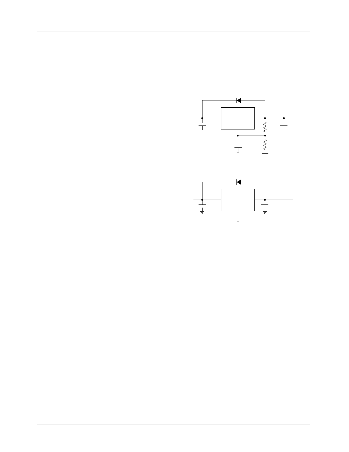
levels of current; a diode from output to input is then recommended, as shown in Figure 2. Usually, normal power supply
cycling or system “hot plugging and unplugging” will not
generate current large enough to do any damage.
Figure 2. Optional Protection
Ripple Rejection
In applications that require improved ripple rejection, a bypass
capacitor from the adjust pin of the FAN1084 to ground
reduces the output ripple by the ratio of V
/1.25V. The
OUT
impedance of the adjust pin capacitor at the ripple frequency
should be less than the value of R1 (typically in the range of
100Ω to 120Ω) in the feedback divider network in Figure 2.
Therefore, the value of the required adjust pin capacitor is a
function of the input ripple frequency. For example, if R1
equals 100Ω and the ripple frequency equals 120Hz, the
adjust pin capacitor should be 22µF. At 10kHz, only 0.22µF is
needed.
Output Voltage
The FAN1084 regulator develops a 1.25V reference voltage
between the ouput pin and the adjust pin (see Figure 3). Placing
a resistor R1 between these two terminals causes a constant
current to flow through R1 and down through R2 to set the
overall output voltage. Normally, this current is the specified
minimum load current of 10mA.
4 REV. 1.0.6 11/18/02
 Loading...