

Fairchild Semiconductor DM96LS02N, DM96LS02MX, DM96LS02M Datasheet

© 2000 Fairchild Semiconductor Corporation DS009816 www.fairchildsemi.com
October 1988
Revised March 2000
DM96LS02 Dual Retriggerable Resettable Monostable Multivibrato r
DM96LS02
Dual Retriggerable Resettable Monostable Multivibrator
General Description
The DM96LS02 is a dual retriggerable and resettable
monostable multivibrator. The one-shot provides exceptionally wide delay range, pulse width stability, predictable
accuracy and immunity to noise . The puls e width is set by
an external resistor and capacitor. Resistor values up to 1.0
MΩ reduce required capacitor values. Hysteresis is provided on both trigger inputs of the DM96LS02 for increased
noise immunity.
Features
■ Required timing capaci t ance r edu ced by factors of 10 to
100 over conventional designs
■ Broad timing resistor range—1.0 kΩ to 2.0 MΩ
■ Output Pulse Width is variable over a 2000:1 range b y
resistor control
■ Propagation delay of 35 ns
■ 0.3V hysteresis on trigger inputs
■ Output pulse width independent of duty cycle
■ 35 ns to ∞ output pulse width range
Ordering Code:
Devices also availab le in Tape and Reel. Specify by appending th e s uffix let t er “X” to the ordering code.
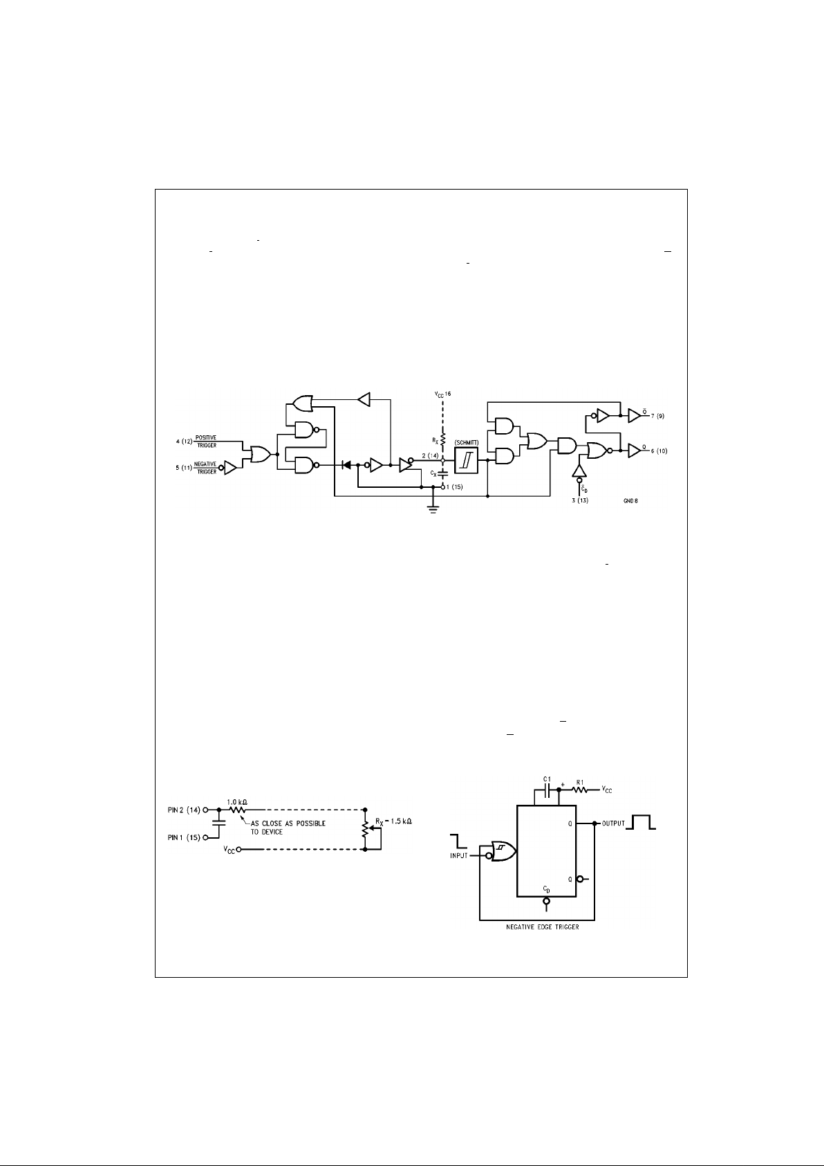
Logic Symbol
VCC = Pin 16
GND = Pin 8
Pin Descriptions
Connection Diagram
Order Number Package Number Package Description
DM96LS02M M16A 16-Lead Small Outline Integrated Circuit (SOIC), JEDEC MS-012, 0.150 Narrow
DM96LS02N N16E 16-Lead Plastic Dual-In-Line Package (PDIP), JEDEC MS-001, 0.300 Wide
Pin
Names
Description
I
0 Trigger Input (Active Falling Edge)
I
0 Schmitt Trigger Input (Active Falling Edge)
I1 Schmitt Trigger Input (Active Rising Edge)
C
D
Direct Clear Input (Active LOW)
Q True Pulse Output
Q
Complementary Pulse Output
www.fairchildsemi.com 2
DM96LS02
Functional Description
The DM96LS02 dua l retriggerable resettable m onostable
multivibrator has two DC coupled trigger inputs p er function, one active L OW (I
0) and one active HIGH (I1). The I1
input and I
0 input of the DM96LS02 utilize an internal
Schmitt trigger with hysteresis of 0.3V to provide increased
noise immunity. The use of active HIGH an d LOW inputs
allows either ris ing or falling edge trigge ring and optional
non-retriggerable operation. The inputs are DC coupled
making triggering independent of input transition times.
When input conditions fo r triggering are met, the Q outp ut
goes HIGH and the external capacitor is rapidly discharged
and then allowed to recharge. An input trigger which occurs
during the timing cycle will retrigger the circuit and re sult in
Q remaining HIG H . T he out pu t pu ls e ma y be ter mi n at e d ( Q
to the LOW state) at any time by settin g the Direct Clear
input LOW. Retriggering may be inhibited by tying the Q
output to I0 or the Q output to I1. Differentia l sensing te chniques are used to obtain excellent stability over temperature and power supply variations and a feedback
Darlington capacitor discharge circuit minimizes pulse
width variation from unit to unit. Schottky TTL output stages
provide high switching speeds and output compatibility with
all TTL logic families.
Logic Diagram
Operation Notes
TIMING
1. An external resistor (R
X
) and an external capacitor (CX)
are required as shown in the Logic Diagram. The value of
R
X
may vary from 1.0 kΩ to 1.0 MΩ.
2. The value of C
X
may vary from 0 to any necessary value
available. If, however, the capacitor has significant leakage
relative to V
CC/RX
the timing equations may n ot represent
the pulse width obtained.
3. The output pulse width t
W
for RX ≥ 10 kΩ an d CX ≥
1000 pF is determined as follows:
t
W
= 0.43 RXC
X
Where RX is in kΩ, CX is in pF, t is in ns or RX is in kΩ, C
X
is in µF, t is in ms.
4. The output pulse widt h for R
X
< 10 kΩ or CX < 1000 pF
should be determ ined from pulse width versus C
X
or R
X
graphs.
5. To obtain variable pulse width by remote trimming, the
following circuit is recommended:
6. Under any operating condition, C
X
and RX (Min) must be
kept as close to the circuit as possible to minimize stray
capacitance and reduce noise pickup.
7. V
CC
and ground wiring should conform to good high fre-
quency standards so that switching transi ents on V
CC
and
ground leads do not cause interaction between one shots.
Use of a 0.01 µF to 0.1 µF bypass capacitor between V
CC
and ground located near the circuit is recommended.
TRIGGERING
1. The minimum ne gative p ulse width into I
0 is 8.0 ns; the
minimum positive pulse width into I1 is 12 ns.
2. Input signals to the DM96LS 02 exhibiting slow or noisy
transitions can use either trigger as both are Schmitt triggers.
3. When non-retrigger able operat ion is re quir ed, i.e., when
input triggers are to be ignored during qu asi-stable state,
input latching is used to inhibit retriggering.
4. An overriding active LOW leve l direct clear is provided
on each multivibrator. By applyin g a LO W to the cle ar, any
timing cycle can be terminated or any new cycle inhibited
until the LOW reset input is removed. Trigger inputs will not
produce spikes in the output when the reset is held LOW. A
LOW-to-HIGH transition on C
D
will not trigger the
DM96LS02. If the C
D
input goes HIGH coincident with a
trigger transition, the circuit will respond to the trigger.
3 www.fairchildsemi.com
DM96LS02
Operation Notes (continued)
Triggering Truth Table
H = HIGH Voltage Level ≥ V
IH
L = LOW Voltage Level ≤ V
IL
X = Immaterial (either H or L)
H→L = HIGH-to-LOW Voltage Level Transit ion
L→H = LOW-to-HIGH Voltage Level Tran si ti on
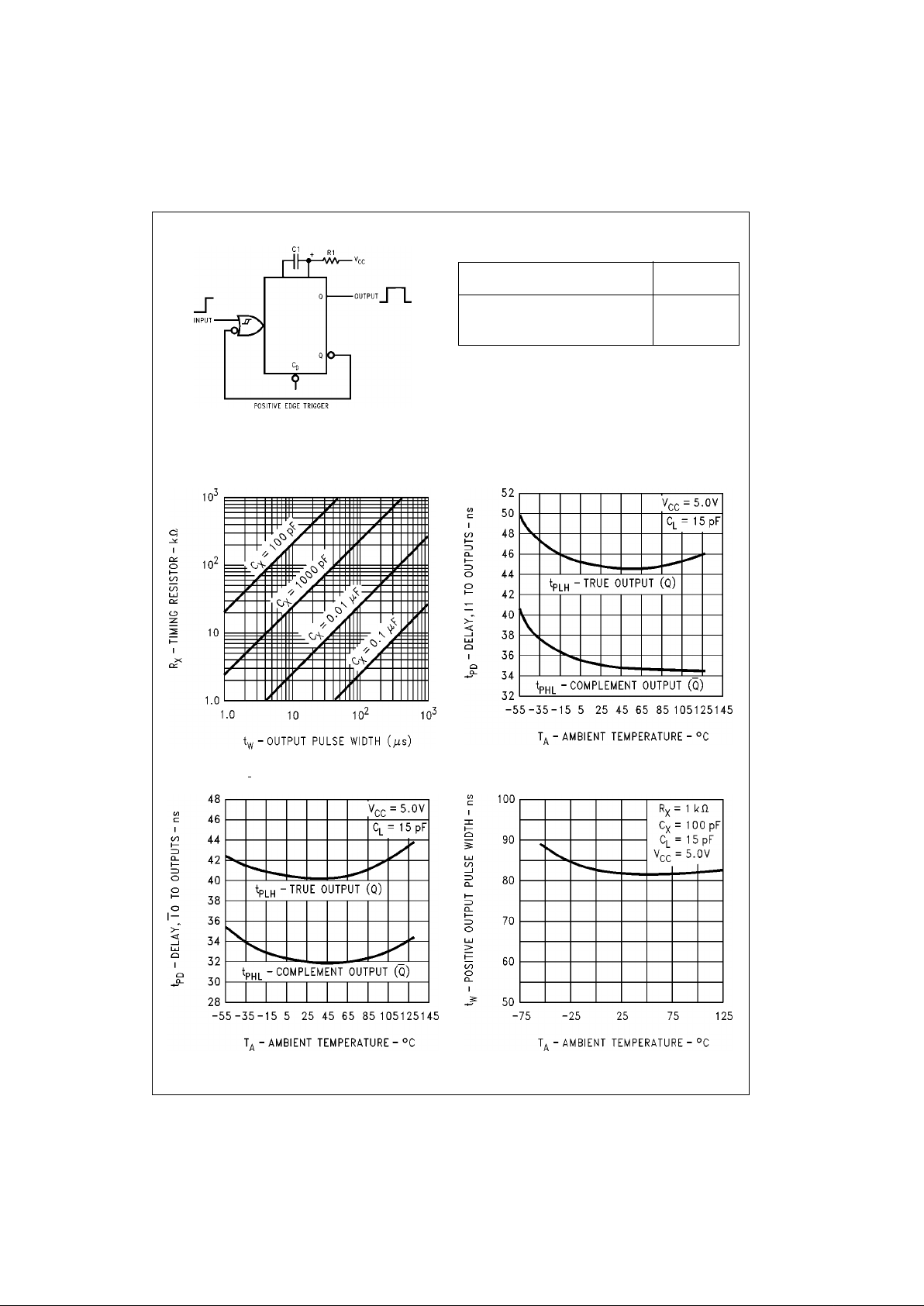
Typical Performance Characteristics
Output tW vs. RX and C
X
I1 Delay Time vs. T
A
I0 Delay Time vs. T
A
Output tW vs. T
A
Pin Numbers
Operation
5(11) 4(12) 3(13)
H→L L H Trigger
HL→HHTrigger
X X L Reset
 Loading...