

Fairchild Semiconductor DM74S257N, DM74S257CW Datasheet
© 2000 Fairchild Semiconductor Corporation DS006482 www.fairchildsemi.com
August 1986
Revised May 2000
DM74S257 3-STATE Quad 1-of-2 Data Selector/Multiplexer
DM74S257
3-STATE Quad 1-of-2 Data Selector/Multiplexer
General Description
These Schottky-clamped high-performance multiplexers
feature 3-STATE outputs that can interface directly with
data lines of bus-organized systems. With all but one of the
common outputs disabl ed (a t a h igh imp edance state) , the
low impedance of the single enabled output will drive the
bus line to a HIGH or LOW logic level. To minimize the possibility that two outputs will attempt to take a common bus
to opposite logic levels, the output enable circuitry is
designed such that the output disable times are shorter
than the output enable times.
This 3-STATE output feature means that n-bi t (paralleled)
data selectors with up to 258 sou rces can be impl ement ed
for data buses. It also permits the use of standard TTL registers for data retention throughout the system.
Features
■ 3-STATE versions S157, S158, with same pin-outs
■ Schottky-clamped for significant improvement in
A-C performance
■ Provides bus interface from multiple sources in high-performance systems
■ Average propagation delay from da ta input 4.8 ns
■ Typical power dissipation 320 mW
Ordering Code:
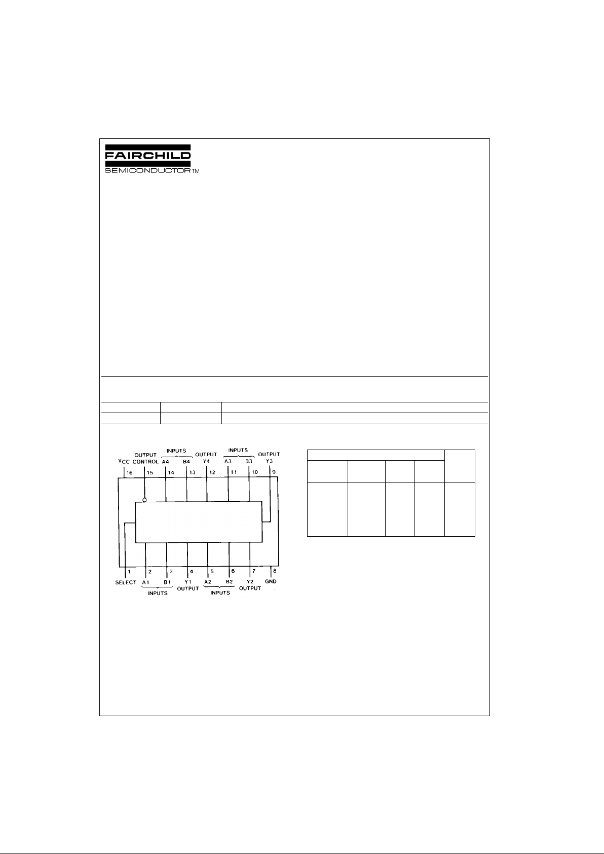
Connection Diagram Function Table
H = HIGH Level
L = LOW Level
X = Don’t Care
Z = High Impedance (OFF)
Order Number Package Number Package Description
DM74S257N N16E 16-Lead Plastic Dual-In-Line Package (PDIP), JEDEC MS-001, 0.300 Wide
Inputs Output
Output Select A B Y
Control
HXXXZ
LLLXL
LLHXH
LHXLL
LHXHH
www.fairchildsemi.com 2
DM74S257
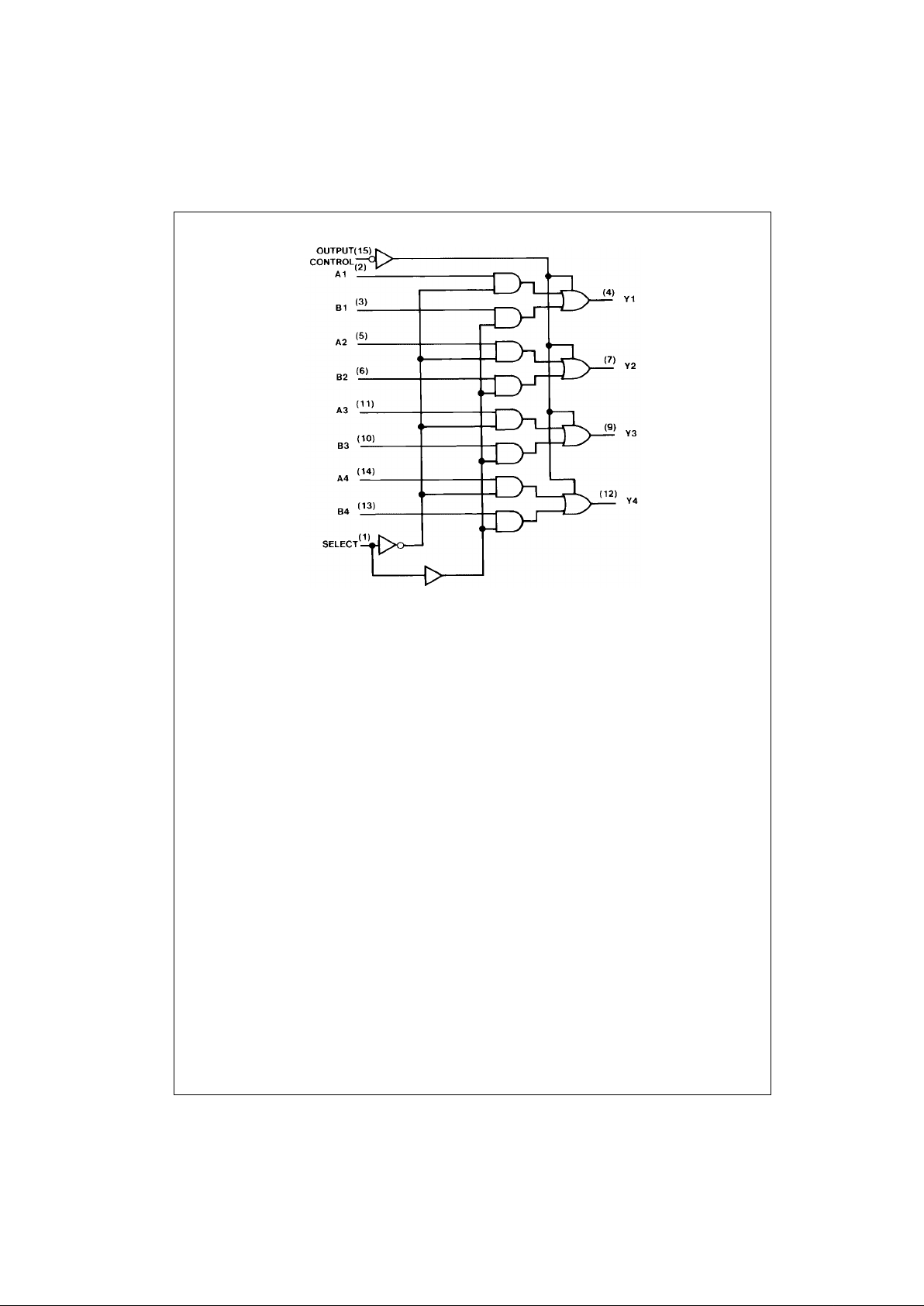
Logic Diagram
 Loading...