

Fairchild Semiconductor DM74S253N Datasheet
August 1986
Revised May 2000
DM74S253
Dual 3-STATE 1-of-4 Line Data Selector/Multiplexer
DM74S253 Dual 3-STATE 1-of-4 Line Data Selector/Multiplexer
General Description
Each of these Schottky-clamped data sele ctors/multiplexers contains inverter s and drivers to supply fu lly complementary, on-chip, binary decoding data selection to the
AND-OR gates. Separate output control inputs are provided for each of the two four-line sections.
The 3-STATE output s can interface dire ctly with data lines
of bus-organized syste ms. With a ll but one of the co mmon
outputs disabled (at a high impedance state), the low
impedance of the single enable output will drive the bus
line to a HIGH or LOW logic level.
Features
■ 3-STATE version of S153 with same pin-out
■ Schottky-diode-clamp ed tra nsistors
■ Permits multiplexing from N lines to 1 line
■ Performs parallel-T-serial conversion
■ Strobe/output control
■ High fan-out totem-pole outputs
■ Typical propagation delay
From data to output 6 ns
From select to output 12 ns
■ Typical power dissipation 275 mW
Ordering Code:
Order Number Package Number Package Description
DM74S253N N16E 16-Lead Plastic Dual-In-Line Package (PDIP), JEDEC MS-001, 0.300 Wide
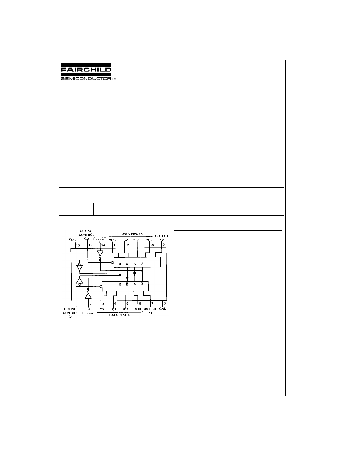
Connection Diagram Function Table
Select Data Inputs Output Output
Inputs Control
B A C0 C1 C2 C3 G Y
XXXXXX H Z
LLLXXX L L
LLHXXX L H
LHXLXX L L
LHXHXX L H
HLXXLX L L
HLXXHX L H
HHXXXL L L
HHXXXH L H
Address inputs A and B are common to bot h s ec t ions.
H = HIGH Level
L = LOW Level
X = Don’t Care
Z = High Impedance
© 2000 Fairchild Semiconductor Corporation DS006481 www.fairchildsemi.com
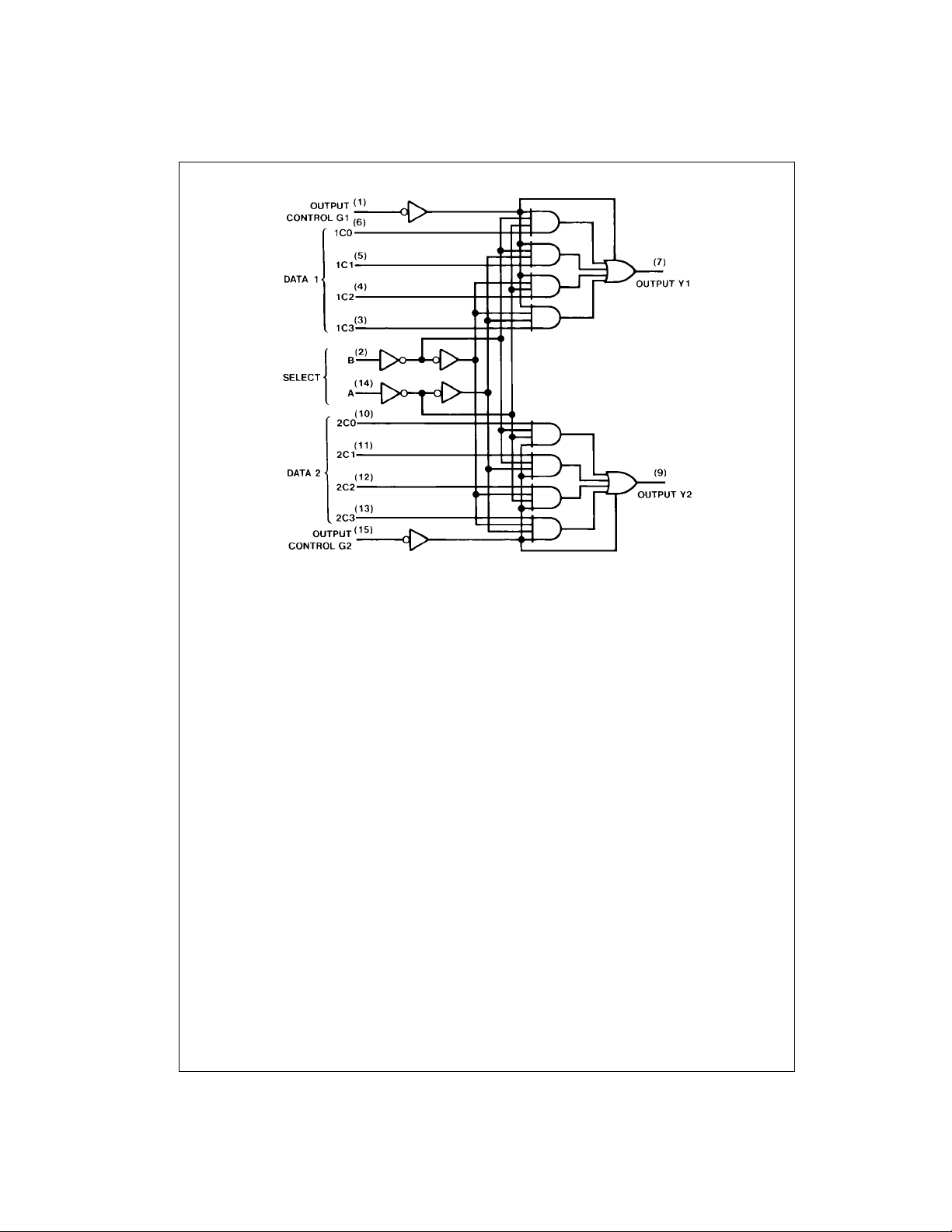
Logic Diagram
DM74S253
www.fairchildsemi.com 2
 Loading...