

Fairchild Semiconductor DM74S244N, DM74S244CW Datasheet
© 2000 Fairchild Semiconductor Corporation DS006478 www.fairchildsemi.com
August 1986
Revised May 2000
DM74S240 • DM74S241 • DM74S244 Octal 3-STATE Buffer/Line Driver/Line Receiver
DM74S240 • DM74S241 • DM74S244
Octal 3-STATE Buffer/Line Driver/Line Receiver
General Description
These buffers/line drivers are designed to improve both the
performance and PC board density of 3-STATE buffers/
drivers employed as memor y-address drivers, clock drivers, and bus-oriented transmitters/receivers. Featuring 400
mV of hysteresis at each low cu rrent PNP data lin e input,
they provide improve d noi se re jection and high fanout outputs, and can be used t o drive terminated lines down to
133Ω.
Features
■ 3-STATE outputs drive bus lines directly
■ PNP inputs reduce DC loading on bus lines
■ Hysteresis at data inputs improves noise margins
■ Typical I
OL
(sink current) 64 mA
■ Typical I
OH
(source current) −15 mA
■ Typical propagation delay times
Inverting 4.5 ns
Noninverting 6 ns
■ Typical enable/disable times 9 ns
■ Typical power dissipation (enabled)
Inverting 450 mW
Noninverting 538 mW
Ordering Code:
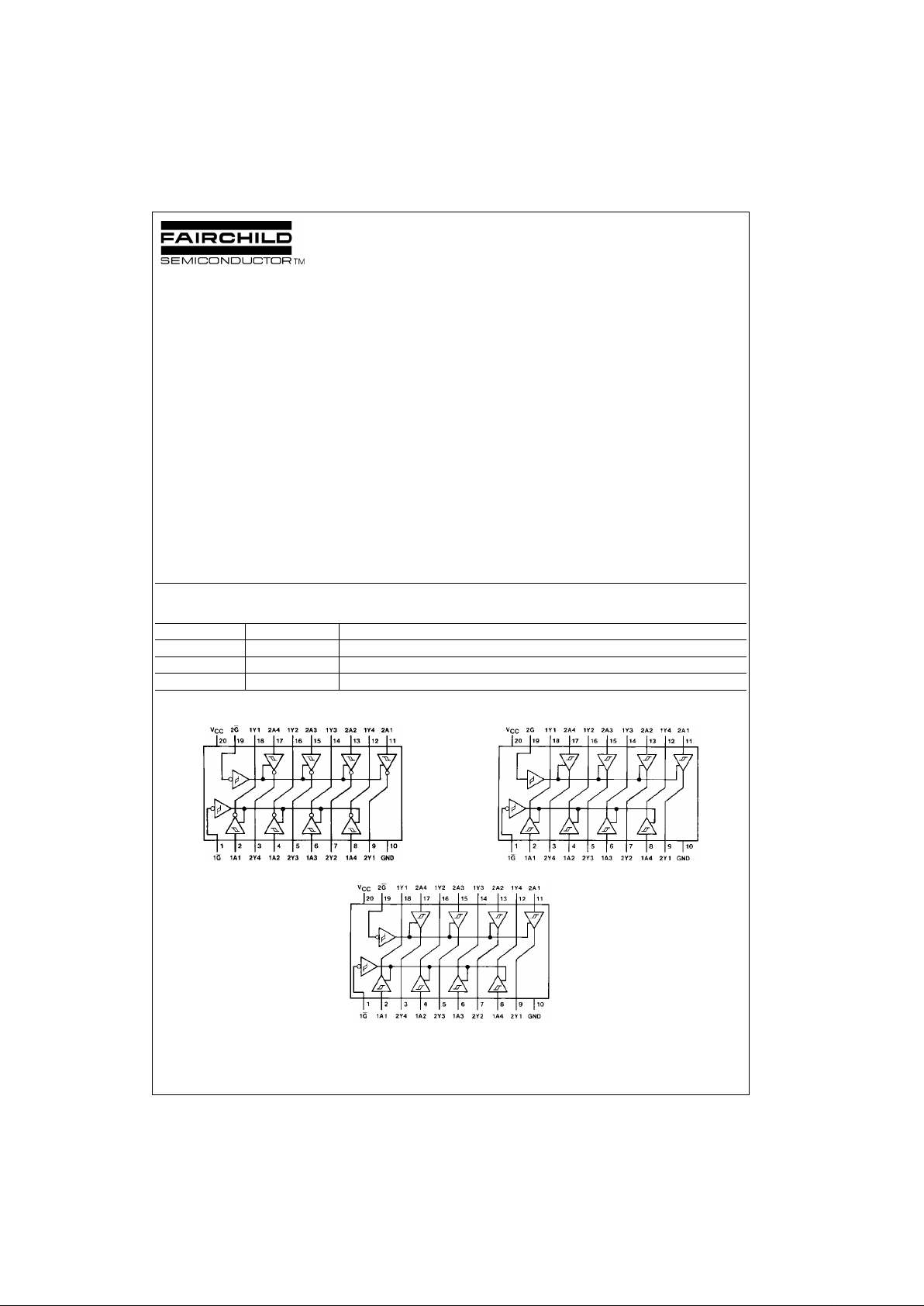
Connection Diagrams
DM74S240N
DM74S241N
DM74S244N
Order Number Package Number Package Description
DM74S240N N20A 20-Lead Plastic Dual-In-Line Package (PDIP), JEDEC MS-001, 0.300 Wide
DM74S241N N20A 20-Lead Plastic Dual-In-Line Package (PDIP), JEDEC MS-001, 0.300 Wide
DM74S244N N20A 20-Lead Plastic Dual-In-Line Package (PDIP), JEDEC MS-001, 0.300 Wide
www.fairchildsemi.com 2
DM74S240 • DM74S241 • DM74S244
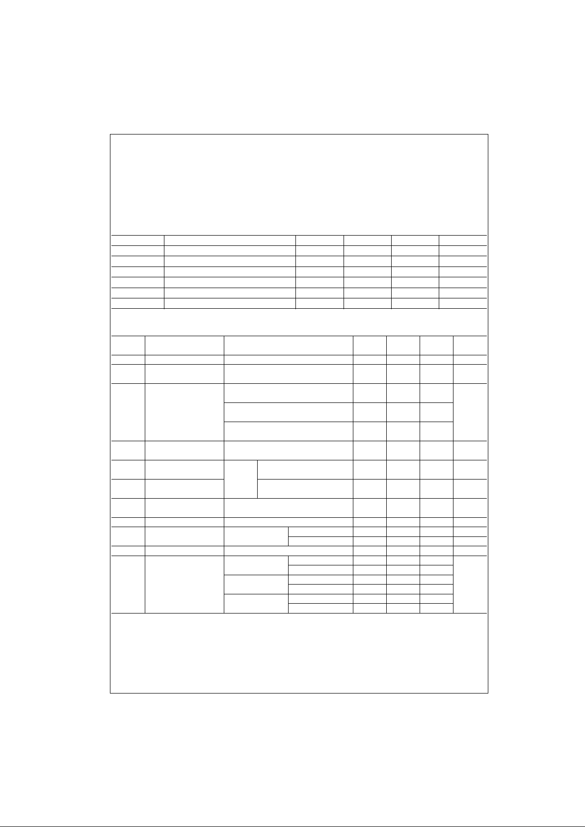
Absolute Maximum Ratings(Note 1)
Note 1: The “Absolute Maxim um Ratin gs” are those valu es beyon d which
the safety of the dev ice cannot be guaranteed. T he device sh ould not be
operated at these limit s. The parametric values defin ed in the Electrical
Characteristics tables are not guaranteed at the absolute maximum ratings.
The “Recommend ed O peratin g Cond itions” t able w ill defin e the co ndition s
for actual device operation.
Recommended Operating Conditions
Electrical Characteristics
over recommended operating free-air temperature range (unless otherwise noted)
Note 2: All typical values are at VCC = 5V, TA = 25°C.
Note 3: Not more than one output should be shorted at a t im e and duration should no t e x ce ed one second.
Supply Voltage 7V
Input Voltage 5.5V
Operating Free Air Temperature Range 0°C to +70°C
Storage Temperature Range −65°C to +150°C
Symbol Parameter Min Typ Max Units
V
CC
Supply Voltage 4.75 5 5.25 V
V
IH
HIGH Level Input Voltage 2 V
V
IL
LOW Level Input Voltage 0.8 V
I
OH
HIGH Level Output Current −15 mA
I
OL
LOW Level Output Current 64 mA
T
A
Free Air Operating Temperature 0 70 °C
Symbol Parameter Conditions Min
Typ
Max Units
(Note 2)
V
I
Input Clamp Voltage VCC = Min, II = −18 mA −1.2 V
H
ys
Hysteresis (VT+ − VT−)VCC = Min 0.2 0.4 V
(Data Inputs Only)
V
OH
HIGH Level VCC = 4.75V, VIH = 2V
2.7
V
Output Voltage VIL = 0.8V, IOH = −1 mA
V
CC
= Min, VIH = 2V
2.4 3.4
V
IL
= 0.8V, IOH = −3 mA
VCC = Min, VIH = 2V
2
V
IL
= 0.5V, IOH = Max
V
OL
LOW Level VCC = Min IOL = Max
0.55 V
Output Voltage VIL = 0.8V, VIH = 2V
I
OZH
Off-State Output Current, VCC = Max VO = 2.4V
50 µA
HIGH Level Voltage Applied V
IL
= 0.8V
I
OZL
Off-State Output Current, VIH = 2V VO = 0.5V
−50 µA
LOW Level Voltage Applied
I
I
Input Current at Maximum VCC = Max VI = 5.5V 1 m A
Input Voltage
I
IH
HIGH Level Input Current VCC = Max VI = 2.7V 50 µA
I
IL
LOW Level Input Current VCC = Max VI = 0.5V Any A −400 µA
Any G −2mA
I
OS
Short Circuit Output Current VCC = Max (Note 3) −50 −225 mA
I
CC
Supply Outputs HIGH DM74S240 80 135
mA
Current DM74S241, DM74244 95 160
Outputs LOW DM74S240 100 150
DM74S241, DM74244 120 180
Outputs Disabled DM74S240 100 150
DM74S241, DM74S244 120 180
 Loading...