

Fairchild Semiconductor DM74S139N Datasheet
DM74S138 • DM74S139
Decoder/Demultiplexer
DM74S138 • DM74S139 Decoder/Demultiplexer
August 1986
Revised April 2000
General Description
These Schottky-clamped circuits are designed to be used
in high-performance memory-decoding or data-routing
applications, requiring very short propagatio n delay times.
In high-performance memory syste ms these decoder s can
be used to minimize the effects of system decodi ng. When
used with high-speed memories, the dela y times of these
decoders are usually le ss than the typical access time of
the memory. This means that the effective system delay
introduced by the dec oder is negligible.
The DM74S138 decodes one-of-eight lines, based upon
the conditions at the three binary select inputs and the
three enable inputs. Two active-LOW and one active-HIGH
enable inputs reduce the ne ed for externa l gates or inverters when expanding. A 24-line decoder can be implemented with no exte rnal inverters, and a 32-line decoder
requires only one inverte r. An enable input can be used as
a data input for demultiplexing applications.
The DM74S139 compri ses two separate two-line-to-fourline decoders in a single package . The acti ve-L OW enable
input can be us ed a s a d ata li ne in dem ultip lexing a pp lications.
All of these decoders/dem ultiplexers feature fu lly buffered
inputs, presenting only one normalized lo ad to its driving
circuit. All inputs are clamped with high-performance
Schottky diodes to suppress lin e-ringing and simplify system design.
Features
■ Designed specifically for high speed:
Memory decoders
Data transmission systems
■ DM74S138 3-to-8-lin e decoders incorporates 3 enable
inputs to simplify cascading and/or data reception
■ DM74S139 contains two fully independent 2-to-4-line
decoders/demultiplexers
■ Schottky clamped for high performance
■ Typical propagation delay time (3 levels of logic)
DM74S138 8 ns
DM74S139 7.5 ns
■ Typical power dissipation
DM74S138 245 mW
DM74S139 300 mW
Ordering Code:
Order Number Package Number Package Description
DM74S138N N16E 16-Lead Plastic Dual-In-Line Package (PDIP), JEDEC MS-001, 0.300 Wide
DM74S139N N16E 16-Lead Plastic Dual-In-Line Package (PDIP), JEDEC MS-001, 0.300 Wide
© 2000 Fairchild Semiconductor Corporation DS006466 www.fairchildsemi.com
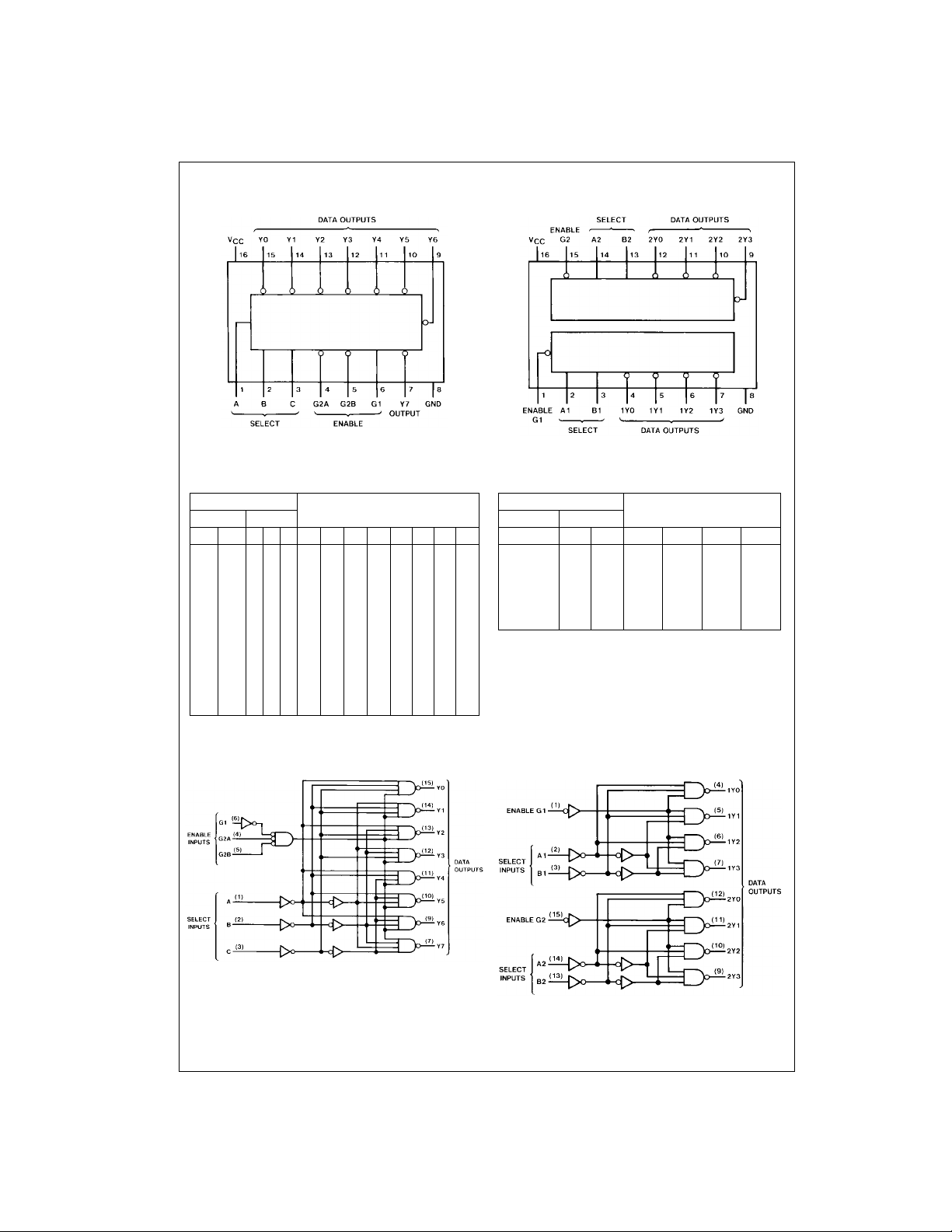
Connection Diagrams
DM74S138 DM74S139
DM74S138 • DM74S139
Function Tables
DM74S138 DM74S139
Inputs
Enable Select
G1 G2* C B A Y0 Y1 Y2 Y3 Y4 Y5 Y6 Y7
X HXXXHHHHHHHH
L XXXXHHHHHHHH
H L LLL L H H H H HH H
HLLLHHLHHHHHH
HLLHLHHLHHHHH
H LLHHHHHLHHHH
H LHLLHHHHLHHH
H LHLHHHHHHLHH
H LHHLHHHHHHLH
H LHHHHHHHHHHL
Outputs
Inputs
Enable Select
G BAY0Y1Y2Y3
H XXHHHH
L LLLHHH
LLHHLHH
LHLHHLH
L HHHHHL
* G2 = G2A + G2B
H = HIGH level
L = LOW level
X = don’t care (either LOW or H I GH logic level)
Outputs
Logic Diagrams
DM74S138 DM74S139
www.fairchildsemi.com 2
 Loading...