

Fairchild Semiconductor DM74S02N, DM74S02CW Datasheet
© 2000 Fairchild Semiconductor Corporation DS006490 www.fairchildsemi.com
August 1986
Revised May 2000
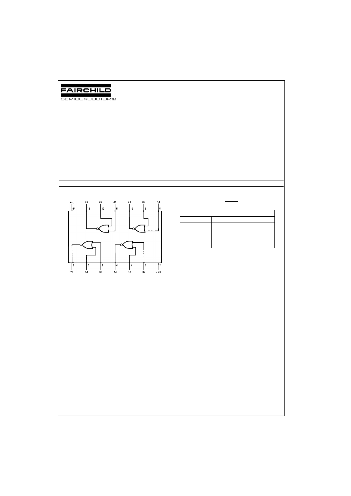
DM74S02 Quad 2-Input NOR Gate
DM74S02
Quad 2-Input NOR Gate
General Description
This device contains four in dep en den t ga tes ea ch of w hich
performs the logic NOR function.
Ordering Code:
Connection Diagram Function Table
H = HIGH Logic Level
L = LOW Logic Level
Order Number Package Number Package Description
DM74S02N N14A 14-Lead Plastic Dual-In-Line Package (PDIP), JEDEC MS-001, 0.300 Wide
Y = A + B
Inputs Output
ABY
LLH
LHL
HLL
HHL
www.fairchildsemi.com 2
DM74S02
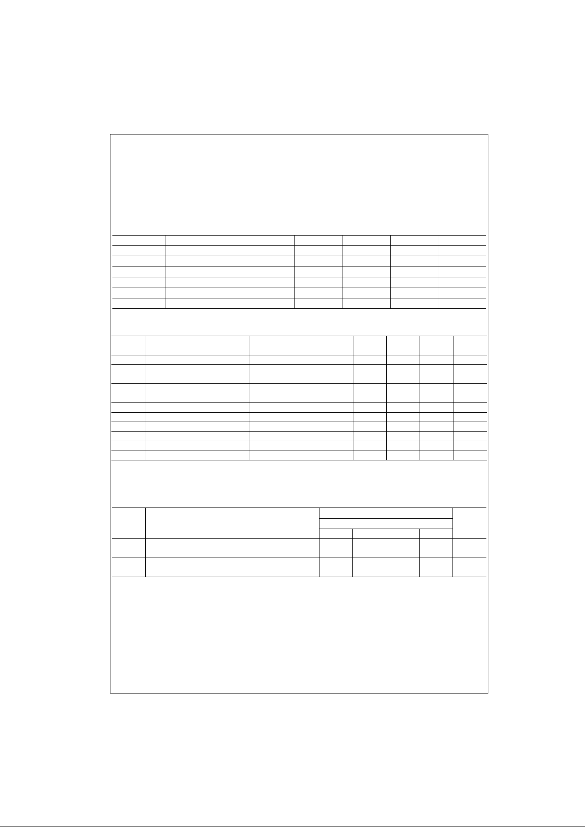
Absolute Maximum Ratings(Note 1)
Note 1: The “Absolute Maximum Ratings” are those values beyond which
the safety of the dev ice cannot be guaranteed. T he device sh ould not be
operated at these limit s. The parametric values defin ed in the Electrical
Characteristics tables are not guaranteed at the absolute maximum ratings.
The “Recommend ed O peratin g Cond itions” t able w ill defin e the co ndition s
for actual device operation.
Recommended Operating Conditions
Electrical Characteristics
over recommended operating free air temperature (unless otherwise noted)
Note 2: All typicals are at VCC = 5V, TA = 25°C.
Note 3: Not more than one output should be shorted at a t im e, and the duration should not exceed one second.
Switching Characteristics
at V
CC
= 5V and T
A
= 25°C
Supply Voltage 7V
Input Voltage 5.5V
Operating Free Air Temperature Range 0°C to +70°C
Storage Temperature Range −65°C to +150°C
Symbol Parameter Min Nom Max Units
V
CC
Supply Voltage 4.75 5 5.25 V
V
IH
HIGH Level Input Voltage 2 V
V
IL
LOW Level Input Voltage 0.8 V
I
OH
HIGH Level Output Current −1mA
I
OL
LOW Level Output Current 20 mA
T
A
Free Air Operating Temperature 0 70 °C
Symbol Parameter Conditions Min
Typ
Max Units
(Note 2)
V
I
Input Clamp Voltage VCC = Min, II = −18 mA −1.2 V
V
OH
HIGH Level VCC = Min, IOH = Max 2.7 3.4
V
Output Voltage VIL = Max
V
OL
LOW Level VCC = Min, IOL = Max
0.5 V
Output Voltage VIH = Min
I
I
Input Current @ Max Input Voltage VCC = Max, VI = 5.5V 1 mA
I
IH
HIGH Level Input Current VCC = Max, VI = 2.7V 50 µA
I
IL
LOW Level Input Current VCC = Max, VI = 0.5V −2mA
I
OS
Short Circuit Output Current VCC = Max (Note 3) −40 −100 mA
I
CCH
Supply Current with Outputs HIGH VCC = Max 17 29 mA
I
CCL
Supply Current with Outputs LOW VCC = Max 26 45 mA
RL = 280Ω
Symbol Parameter CL = 15 pF CL = 50 pF Units
Min Max Min Max
t
PLH
Propagation Delay Time
1.5 5.5 2 7.5 ns
LOW-to-HIGH Level Output
t
PHL
Propagation Delay Time
1.5 5.5 2 7.5 ns
HIGH-to-LOW Level Output
 Loading...