

Fairchild Semiconductor DM74LS123SJX, DM74LS123SJ, DM74LS123N, DM74LS123MX, DM74LS123M Datasheet
...
© 2000 Fairchild Semiconductor Corporation DS006386 www.fairchildsemi.com
August 1986
Revised April 2000
DM74LS123 Dual Retriggerable One-Shot with Clear and Complementary Outputs
DM74LS123
Dual Retriggerable One-Shot
with Clear and Complementary Outputs
General Description
The DM74LS123 is a dual retriggerabl e monostable mu ltivibrator capable of gen erating output pulses from a few
nano-seconds to ex tremely lo ng dura tion up t o 100 % duty
cycle. Each device has three inputs permitting the choice of
either leading edge or trail ing edge trigg erin g. Pin (A) is an
active-LOW transition t rigg er in pu t and pin (B) is an activeHIGH transition trigger inpu t. The clear (CLR) inp ut terminates the output pulse at a predetermined time independent of the timing comp one nts. The clear input also ser ves
as a trigger input when it is pulsed with a low level pulse
transition (
). To obtain the best trouble free ope ration
from this device please read th e oper ating ru les as well as
the Fairchild Semiconductor one-shot application notes
carefully and observe recommendations.
Features
■ DC triggered from active- HIGH tra nsition or active-LO W
transition inputs
■ Retriggerable to 100% duty cycle
■ Compensated for V
CC
and temperature variations
■ Triggerable from CLEAR input
■ DTL, TTL compatible
■ Input clamp diodes
Ordering Code:
Devices also availab le in Tape and Reel. Specify by appending th e s uffix let t er “X” to the ordering code.
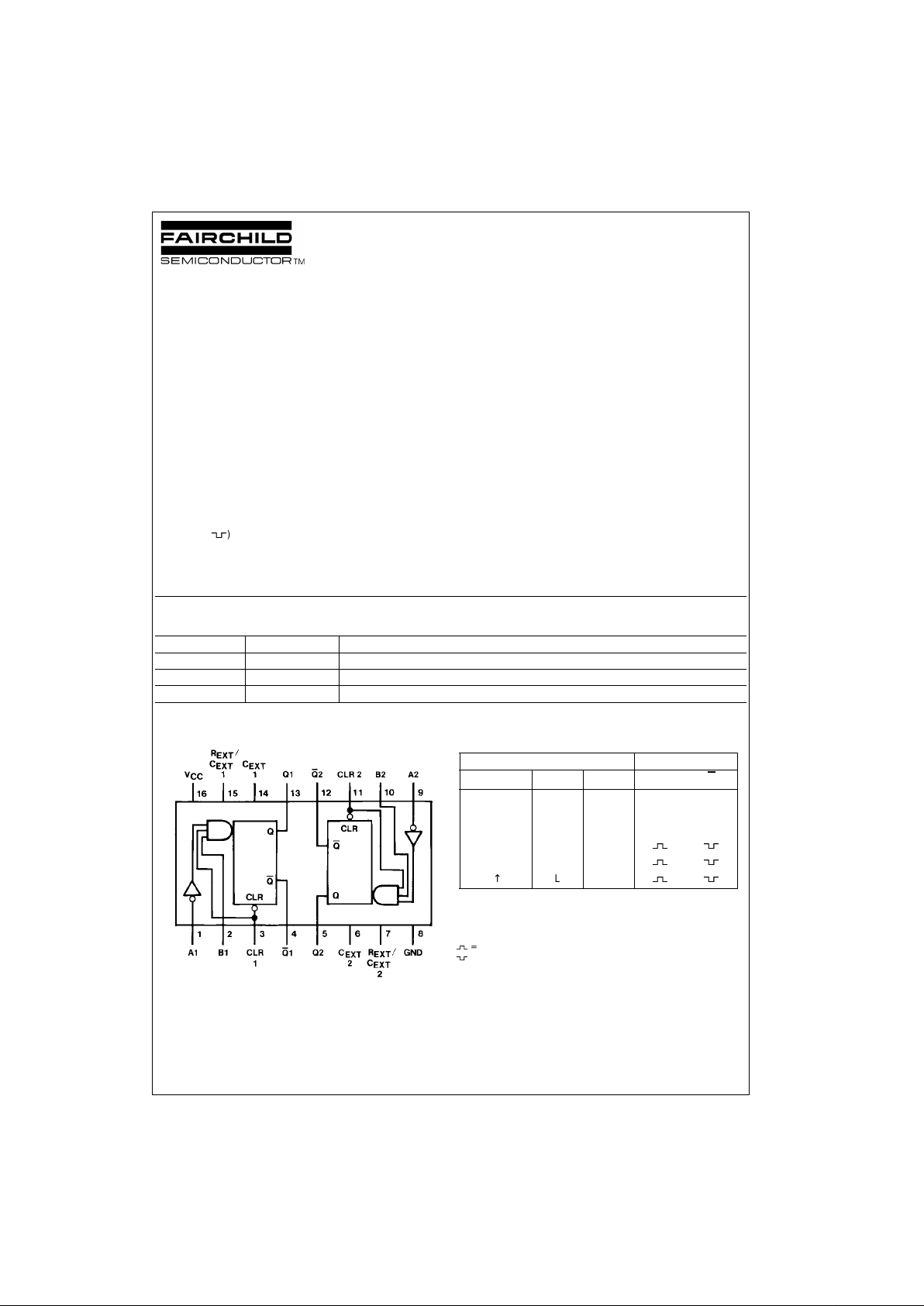
Connection Diagram Function Table
H = HIGH Logic Level
L = LOW Logic Level
X = Can Be Either LOW or HIGH
↑ = Positive Going Transition
↓ = Negative Going Trans it ion
= A Positive Pulse
= A Negative Pulse
Order Number Package Number Package Description
DM74LS123M M16A 16-Lead Small Outline Integrated Circuit (SOIC), JEDEC MS-012, 0.150 Narrow
DM74LS123SJ M16D 16-Lead Small Outline Package (SOP), EIAJ TYPE II, 5.3mm Wide
DM74LS123N N16E 16-Lead Plastic Dual-In-Line Package (PDIP), JEDEC MS-001, 0.300 Wide
Inputs Outputs
CLEAR A B Q Q
LXXLH
XHXLH
XXLLH
HL↑
H ↓ H
↑ LH

www.fairchildsemi.com 2
DM74LS123
Functional Description
The basic output pulse width is determined by selection of
an external resistor (R
X
) and capacitor (CX). Once trig-
gered, the basic pulse width may be extended by retriggering the gated active-LOW transition or active-HIGH
transition inputs or be reduced by use of the active-LOW or
CLEAR input. Retrigger ing to 100% duty cycle i s possible
by application of an input pulse train whose c ycle time is
shorter than the output cycle time suc h that a continu ous
“HIGH” logic state is maintained at the “Q” output.
Operating Rules
1. An external res isto r (RX) and an external capacitor (CX)
are required for pr op er o per ation. The value of C
X
may
vary from 0 to any necessary value. For small time constants high-grade mica, glass, polypr opylene, polycar bonate, or polystyrene material capacitors may be
used. For large time constants use tantalum or special
aluminum capacitors. If the timing capacitors have
leakages approach ing 100 nA or if stray capacitan ce
from either terminal to groun d i s grea ter than 50 pF the
timing equations may no t represent the pulse width th e
device generates.
2. When an ele ctrol ytic capa citor i s use d for C
X
a switch-
ing diode is often requir ed for standard TTL one-shots
to prevent high inverse leakage current . Thi s switchin g
diode is not need ed for the DM7 4LS123 one- shot and
should not be used. I n ge ner al th e u se of the sw itchi n g
diode is not recommended with retriggerable operation.
Furthermore, if a polarized timing capacitor is used on
the DM74LS123 the nega tive terminal of th e capacitor
should be connected to the “C
EXT
” pin of the device
(Figure 1).
FIGURE 1.
3. For C
X
>> 1000 pF the output pulse width (tW) is
defined as follows:
t
W
= KRX C
X
where [RX is in kΩ]
[C
X
is in pF]
[t
W
is in ns]
K ≈ 0.37
4. The multiplicative factor K is plotted as a function of C
X
below for design considerations:
FIGURE 2.
5. For C
X
< 1000 pF see Figure 3 for tW vs. CX family
curves with R
X
as a parameter:
FIGURE 3.
6. To obtain variable pulse widths by remote trimming, the
following circuit is recommended:
FIGURE 4.
“R
remote
” should be as close to the device pin as possible.
7. The retrigger able pulse width is calculated as shown
below:
T = t
W
+ t
PLH
= K × RX × CX + t
PLH
The retriggered pulse width is equ al to the pulse width
plus a delay time period (Figure 5).
FIGURE 5.
3 www.fairchildsemi.com
DM74LS123
Operating Rules (Continued)
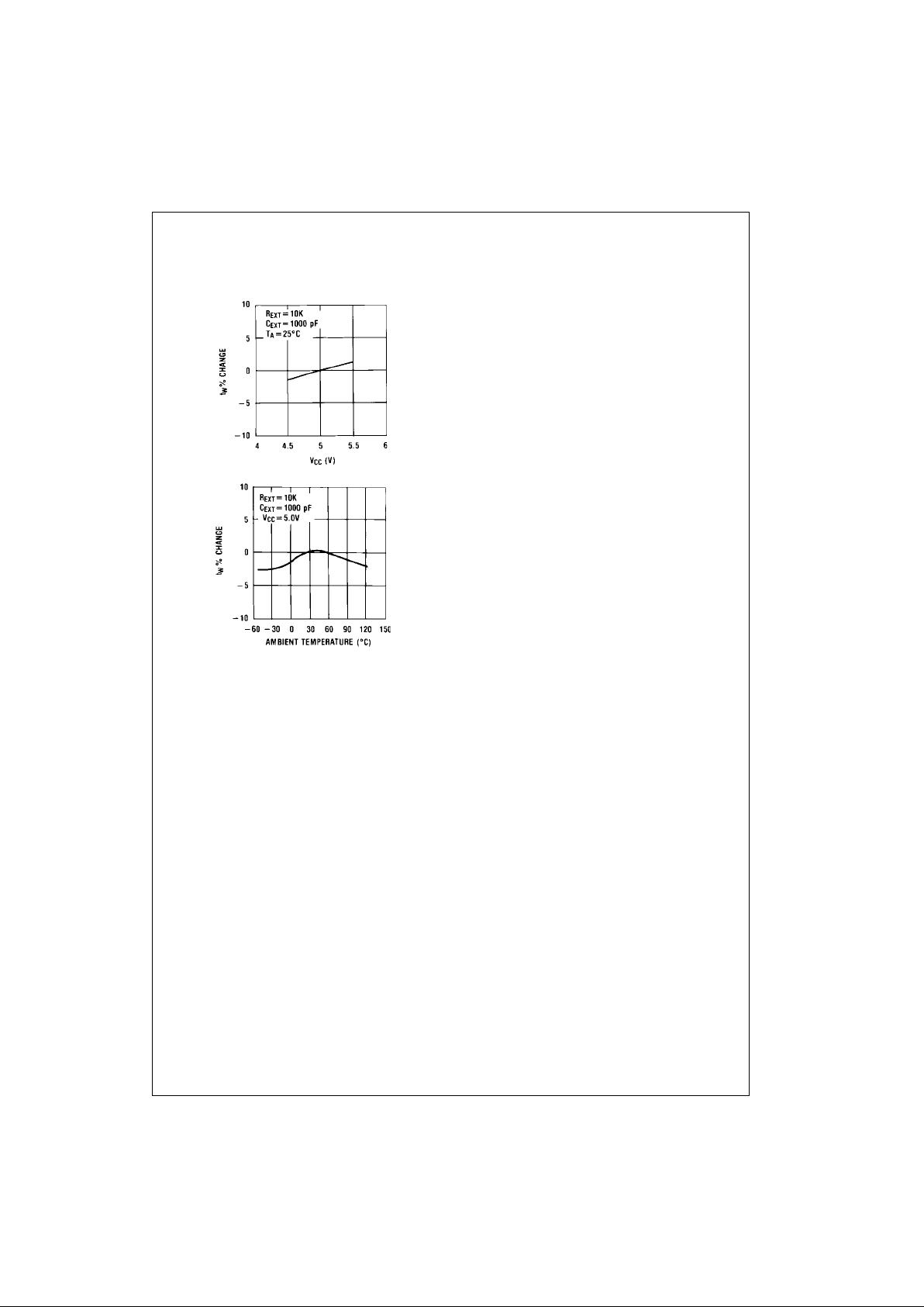
8. Output pulse wid th variation versus V
CC
and tempera-
tures: Figure 6 depicts the relationship between pulse
width variation versus V
CC
, and Figure 7 depicts pulse
width variation versus temperatures.
FIGURE 6.
FIGURE 7.
9. Under any operating condition C
X
and RX must be kept
as close to the one-shot device pins as possible to minimize stray capacitance, to reduce noise pick-up, and
to reduce I-R and Ldi/ dt voltage devel oped along t heir
connecting paths. If the lead len gth from C
X
to pins (6)
and (7) or pins (14) a nd (15) is great er than 3 cm, for
example, the output pulse width might be quite different
from values predicte d from the appropriat e equations.
A non-inductive and low capacitive path is necessary to
ensure complete discharge o f C
X
in each cycle of its
operation so that the output pulse width will be a ccurate.
10. The C
EXT
pins of this device are internally connected to
the internal ground. F or optimum system pe rformance
they should be hard wired to the system’s return
ground plane.
11. V
CC
and ground wiring shoul d conform to good high-
frequency standards and practices so that switching
transients on the V
CC
and ground return lea ds do not
cause inter act ion be tw een on e-sh ots . A 0.0 1 µF to 0.10
µF bypass capacitor (disk cera mic or monolithic type)
from V
CC
to ground is necessary o n each device. Fur-
thermore, the bypass capacitor sho uld be located as
close to the V
CC
-pin as space permits.
Note: For further detailed device characteristics and output performance please refer to the Fairchild Semiconductor one-shot
application note AN-372.
 Loading...