


Fairchild Semiconductor DM74LS112AN, DM74LS112AMX, DM74LS112AM, DM74LS112ACW Datasheet
© 2000 Fairchild Semiconductor Corporation DS006382 www.fairchildsemi.com
August 1986
Revised March 2000
DM74LS112 A Dual Negative-Edge-Triggered Master-Slave J-K Flip-Flop with Preset, Clear, and Complementary
Outputs
DM74LS112A
Dual Negative-Edge-T riggered Master-Slave J-K Flip-Flop
with Preset, Clear, and Complementary Outputs
General Description
This device contains two indepe ndent negative-edge-triggered J-K flip-flops with complementary outputs. The J and
K data is processed by the flip-flop on the falling edge of
the clock pulse. The clock triggering occurs at a volta ge
level and is not directly re lated to the transition time of the
falling edge of the clock pulse. Data on the J and K inputs
may be changed w hile the clock is HIGH or LOW without
affecting the outputs as lo ng as the setup and hold times
are not violated. A low logic lev el on the preset or clear
inputs will set or reset the outputs regardless of the logic
levels of the other inputs.
Ordering Code:
Devices also availab le in Tape and Reel. Specify by appending th e s uffix let t er “X” to the ordering code.
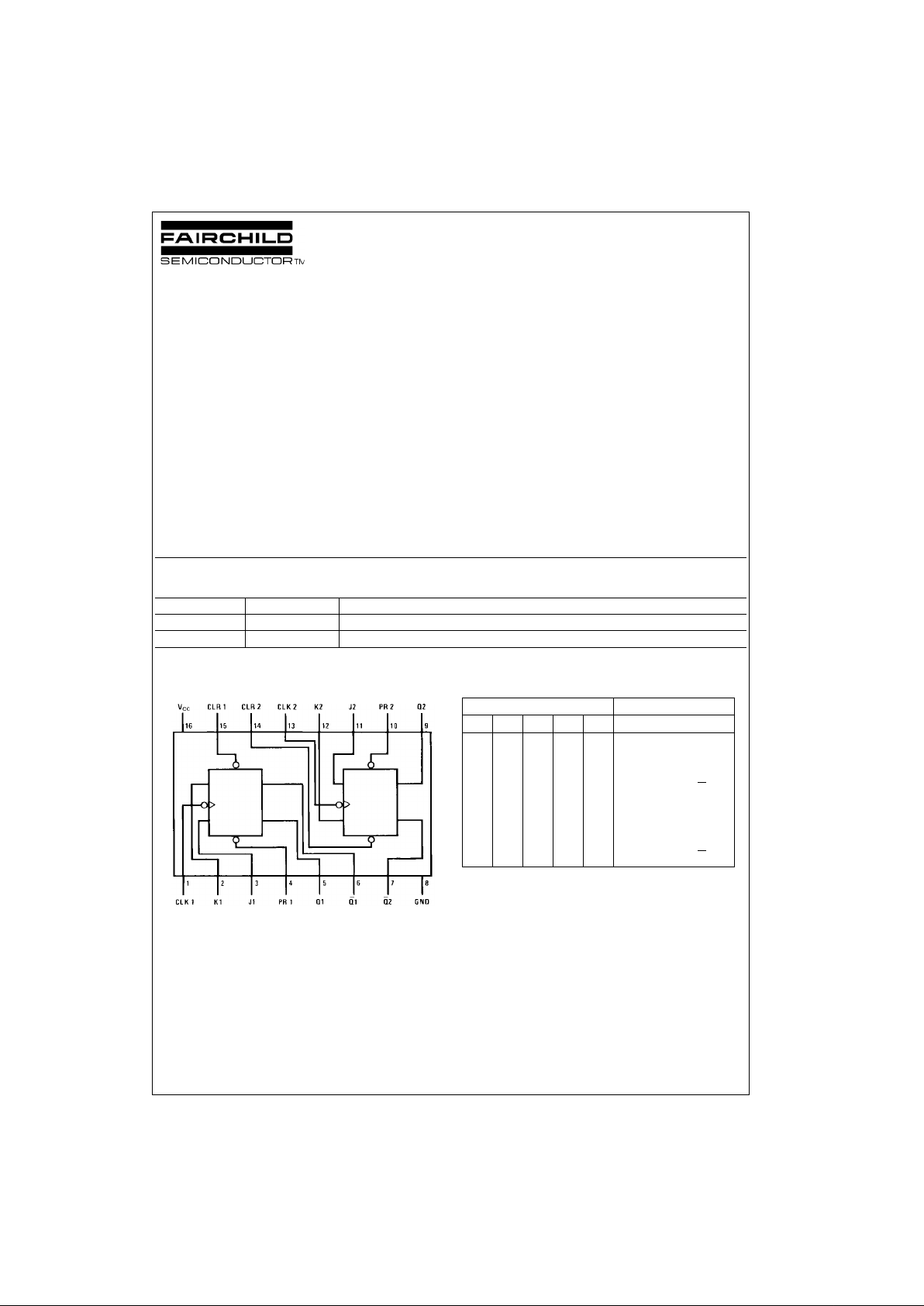
Connection Diagram Function Table
H = HIGH Logic Level
L = LOW Logic Level
X = Either LOW or HIGH Logic Level
↓ = Negative Going Edge of Pulse
Q
0
= Th e output logic level before the indicated input conditions were
established.
Toggle = Each output changes to the complement of its previous level on
each falling edge of th e c loc k pulse.
Note 1: This configuration is nonstable; that is, it will no t persist when
preset and/or clear inputs return to their inact iv e (H I GH) level.
Order Number Package Number Package Description
DM74KS112AM M16A 16-Lead Small Outline Integrated Circuit (SOIC), JEDEC MS-012, 0.150 Narrow
DM74LS112AN N16E 16-Lead Plastic Dual-In-Line Package (PDIP), JEDEC MS-001, 0.300 Wide
Inputs Outputs
PR CLR CLK J K Q Q
LHXXX H L
HLXXX L H
L L X X X H (Note 1) H (Note 1)
HH↓ LL Q
0
Q
0
HH↓ HL H L
HH↓ LH L H
HH↓ HH Toggle
HHHXX Q
0
Q
0
www.fairchildsemi.com 2
DM74LS112A
Absolute Maximum Ratings(Note 2)
Note 2: The “Absolute Maximum Ratin gs” are those v alues beyon d which
the safety of the dev ice cannot be guaranteed. T he device sh ould not be
operated at these limits. The parametric values defined in the Electrical
Characteristics tables are not guaranteed at the absolute maximum ratings.
The “Recommend ed O peratin g Cond itions” t able w ill defin e the co ndition s
for actual device operation.
Recommended Operating Conditions
Note 3: CL = 15 pF, RL = 2 kΩ, TA = 25°C and VCC = 5V.
Note 4: The symbol (↓) indicates the falling edge of the clock puls e is used for reference.
Note 5: C
L
= 50 pF, RL = 2 kΩ, TA = 25°C and VCC = 5V.
Supply Voltage 7V
Input Voltage 7V
Operating Free Air Temperature Range 0°C to +70°C
Storage Temperature Range −65°C to +150°C
Symbol Parameter Min Nom Max Units
V
CC
Supply Voltage 4.75 5 5.25 V
V
IH
HIGH Level Input Voltage 2 V
V
IL
LOW Level Input Voltage 0.8 V
I
OH
HIGH Level Output Current −0.4 mA
I
OL
LOW Level Output Current 8 mA
f
CLK
Clock Frequency (Note 3) 0 30 MHz
f
CLK
Clock Frequency (Note 5) 0 25 MHz
t
W
Pulse Width Clock HIGH 20
(Note 3) Preset LOW 25 ns
Clear LOW 25
t
W
Pulse Width Clock HIGH 25
(Note 5) Preset LOW 30 ns
Clear LOW 30
t
SU
Setup Time (Note 3)(Note 4) 20↓ ns
t
SU
Setup Time (Note 4)(Note 5) 25↓ ns
t
H
Hold Time (Note 3)(Note 4) 0↓ ns
t
H
Hold Time (Note 4)(Note 5) 5↓ ns
T
A
Free Air Operating Temperature 0 70 °C