


Fairchild Semiconductor DM74AS240WM, DM74AS240N, DM74AS240WMX Datasheet
© 2000 Fairchild Semiconductor Corporation DS006298 www.fairchildsemi.com
October 1986
Revised March 2000
DM74AS240 • DM74AS244 3-STATE Bus Driver/Receiver
DM74AS240 • DM74AS244
3-STATE Bus Driver/Receiver
General Description
This family of Advance Sc hottky 3-STATE Bus circuits are
designed to provide either bidirectional or unidirectional
buffer interface in Memory, Microprocessor, and Communication Systems. The out put characteristics of the circui ts
have low impedance suffi cient to drive terminated transmission lines down to 133Ω. The input characteristics of
the circuits likewise have a high impedance s o it will not
significantly load the transmission line. The package contains eight 3-STATE buffers organized with four buffers
having a common 3-STATE enable gate. The DM74AS240
and DM74AS244 are eight w ide in a 20 pin package, and
may be used as a 4 wide bid irectional or eight wide un idirectional. The buffer sel ection includes invert ing and noninverting, with enable or disable 3-STATE control.
Features
■ Advanced oxide-isolated, ion-implanted Schottky TTL
process
■ Improved switching per formance with less power dissipation compared with Schottky counterpart
■ Functional and pin compa tible with 74LS and Schottky
counterpart
■ Switching response specified into 500Ω and 50 pF
■ Specified to interface with CMOS at V
OH
= VCC − 2V
Ordering Code:
Devices also availab le in Tape and Reel. Specify by appending th e s uffix let t er “X” to the ordering code.
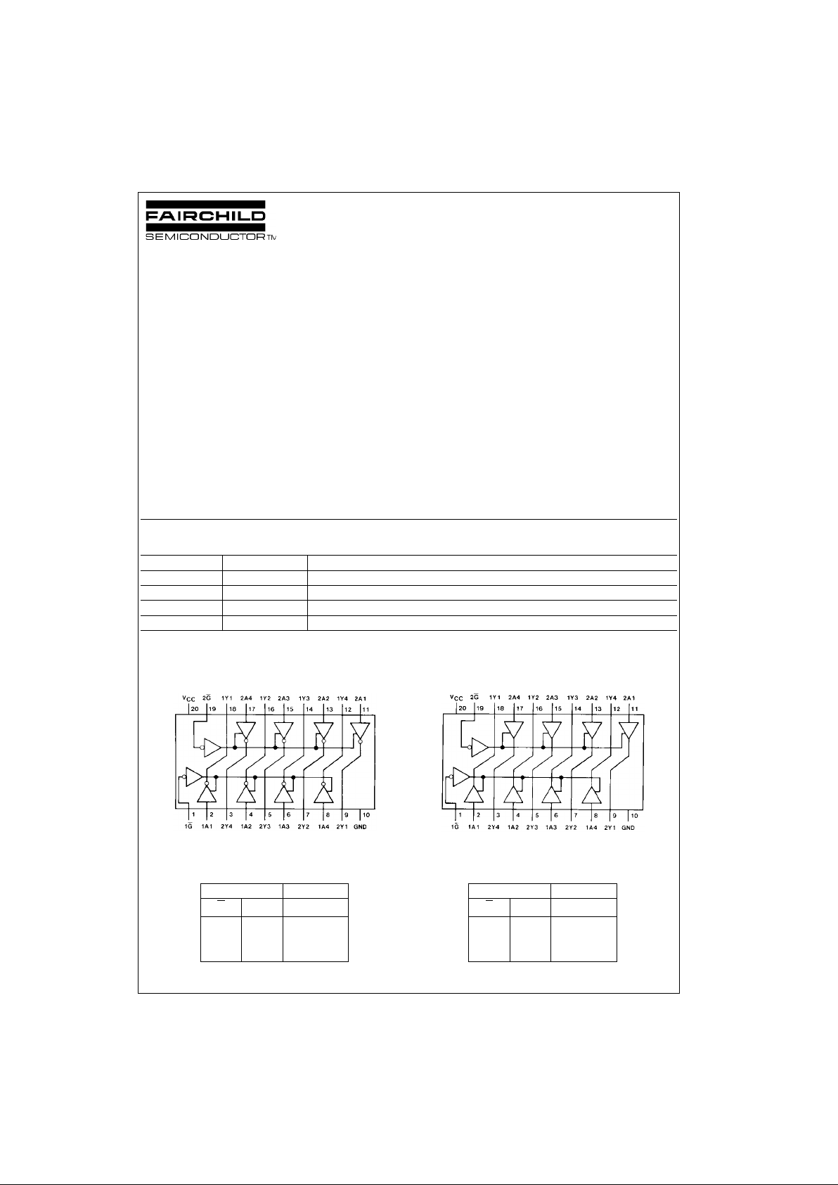
Connection Diagrams
DM74AS240 DM74AS244
Function Tables
DM74AS240 DM74AS244
L = LOW Logic Level H = HIGH Logic Level X = Either LOW or HIGH Lo gic Level Z = High Imp edance
Order Number Package Number Package Description
DM74AS240WM M20B 20-Lead Small Outline Integrated Circuit (SOIC), JEDEC MS-013, 0.300 Wide
DM74AS240N N20A 20-Lead Plastic Dual-In-Line Package (PDIP), JEDEC MS-001, 0.300 Wide
DM74AS244WM M20B 20-Lead Small Outline Integrated Circuit (SOIC), JEDEC MS-013, 0.300 Wide
DM74AS244N N20A 20-Lead Plastic Dual-In-Line Package (PDIP), JEDEC MS-001, 0.300 Wide
Inputs Output
G
AY
LL H
LH L
HX Z
Inputs Output
G
AY
LL L
LH H
HX Z
www.fairchildsemi.com 2
DM74AS240 • DM74AS244
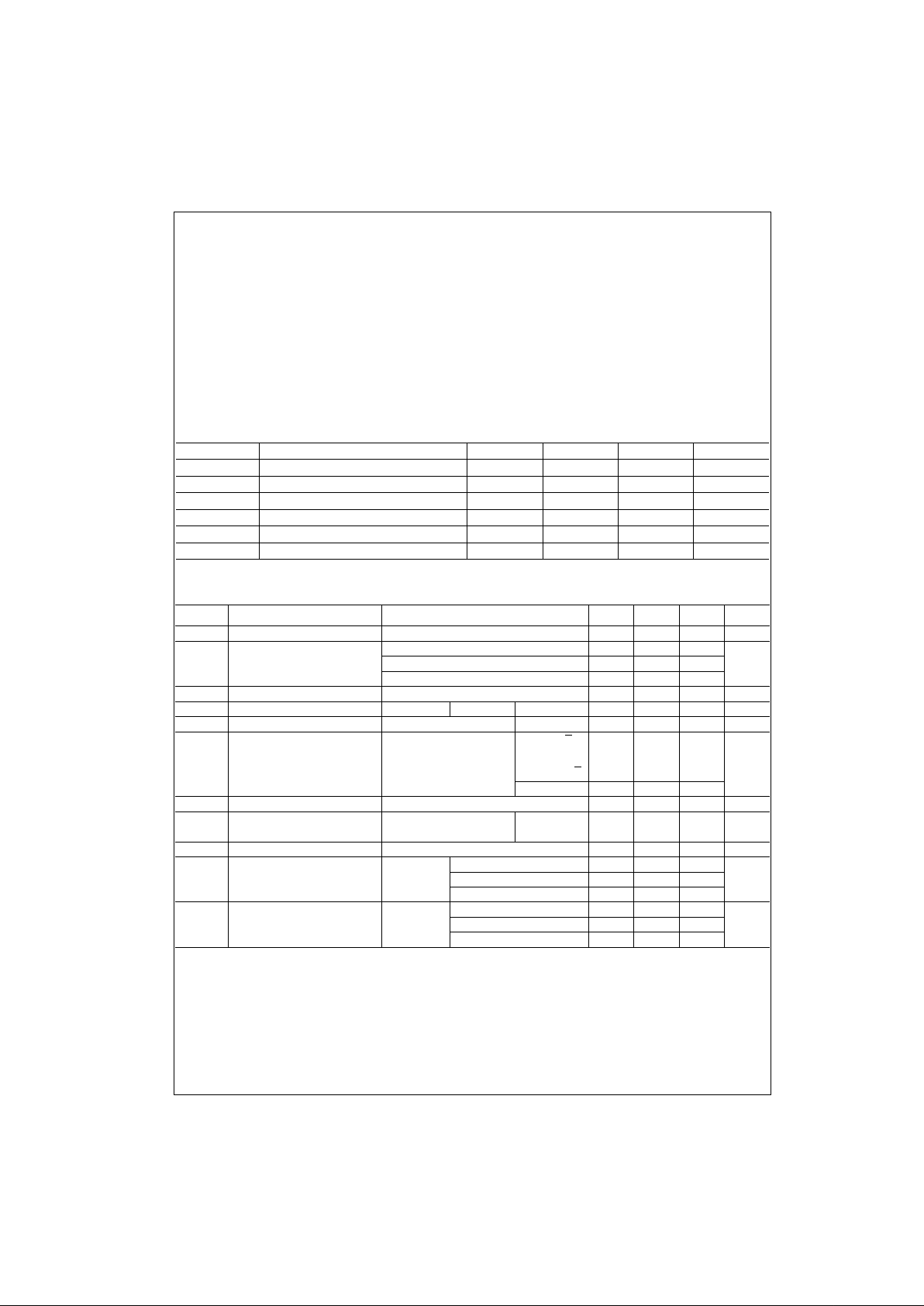
Absolute Maximum Ratings(Note 1)
Note 1: The “Absolute Maximum Ratin gs” are those v alues beyon d which
the safety of the dev ice cannot be guaranteed. T he device sh ould not be
operated at these limits. The parametric values defined in the Electrical
Characteristics tables are not guaranteed at the absolute maximum ratings.
The “Recommend ed O peratin g Cond itions” t able w ill defin e the co ndition s
for actual device operation.
Recommended Operating Conditions
Electrical Characteristics
over recommended operating free air temperature range. All typical values are measured at VCC = 5V, TA = 25°C.
Note 2: The output c onditions have been ch os en to produce a current that closely approximat es one half the true shor t- c irc uit output current, IOS.
Supply Voltage, V
CC
7V
Input Voltage 7V
Voltage Applied to Disabled Output 5.5V
Operating Free Air Temperature Range 0°C to +70°C
Storage Temper ature Range −65°C to +150°C
Typical θ
JA
N Package 57.0°C/W
M Package 76.0°C/W
Symbol Parameter Min Nom Max Units
V
CC
Supply Voltage 4.5 5 5.5 V
V
IH
HIGH Level Input Voltage 2 V
V
IL
LOW Level Input Voltage 0.8 V
I
OH
HIGH Level Output Current −15 mA
I
OL
LOW Level Output Current 64 mA
T
A
Free Air Operating Temperature 0 70 °C
Symbol Parameter Conditions Min Typ Max Units
V
IK
Input Clamp Voltage VCC = 4.5V, IIN = −18 mA −1.2 V
V
OH
HIGH Level VCC = 4.5V, IOH = −3 mA 2.4 3.2
VOutput Voltage VCC = 4.5V, IOH = Max 2.4
IOH = −2 mA, VCC = 4.5V to 5.5V VCC−2
V
OL
LOW Level Output Voltage VCC = 4.5V, IOL = Max 0.35 0.55 V
I
I
Input Current at Max Input Voltage VCC = 5.5V VIN = 7V Others 100 µA
I
IH
HIGH Level Input Current VCC = 5.5V, VIN = 2.7V Others 20 µA
I
IL
LOW Level Input Current VCC = 5.5V, VIN = 0.4V AS240, (G, G),
µA
(Control Inputs), −500
DM74AS244 (G)
DM74AS244 (A) −1000
I
OZH
HIGH Level 3-STATE Output Current VCC = 5.5V, V= 2.7V 50 µA
I
OZL
LOW Level 3-STATE
VCC = 5.5V, V = 0.4V
DM74AS240,
−50 µA
Output Current DM74AS244
IO (Note 2) Output Drive Current VCC = 5.5V, V
OUT
= 2.25V −50 −115 −150 mA
I
CC
DM74AS240 VCC = 5.5V Outputs HIGH 11 17
Supply Current Outputs LOW 51 75 mA
3-STATE 24 38
I
CC
DM74AS244 VCC = 5.5V Outputs HIGH 22 34
Supply Current Outputs LOW 60 90 mA
3-STATE 34 54