

Fairchild Semiconductor DM74AS1804WMX, DM74AS1804WM, DM74AS1804N Datasheet
© 2000 Fairchild Semiconductor Corporation DS008619 www.fairchildsemi.com
July 1985
Revised March 2000
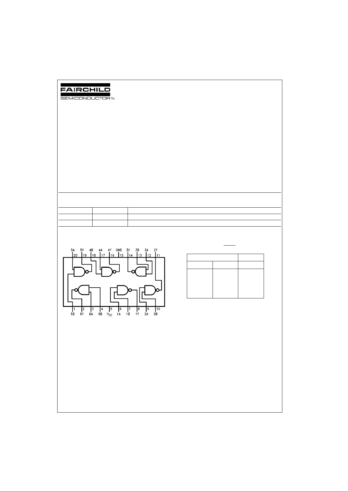
DM74AS1804 Hex 2-Input NAND Driver
DM74AS1804
Hex 2-Input NAND Driver
General Description
These devices contain six independent 2-Input drivers
each of which performs the logic NAND function. The
DM74AS1804 is e quivalent to the DM74AS804B but the
supply voltage and ground p ins are centered in the package. This positioning of the supply voltage and ground pins
reduce the lead inducta nce of t hese pin s . T his r edu ction of
lead inductance will minimize noise generated onto either
the supply voltage or ground bus which is significant in high
current switching applications.
Features
■ Switching specifications at 50 pF
■ Switching specifications guaranteed over full tempera-
ture and V
CC
range
■ Advanced oxide-isolated, ion-implanted Schottky TTL
process
■ Centered V
CC
and GND configuration provides minimum
lead inductance for high current switching applications
■ High capacitive drive capability
Ordering Code:
Devices also availab le in Tape and Reel. Specify by appending th e s uffix let t er “X” to the ordering code.
Connection Diagram Function Table
H = HIGH Logic Level
L = LOW Logic Level
Order Number Package Number Package Description
DM74AS1804WM M20B 20-Lead Small Outline Integrated Circuit (SOIC), JEDEC MS-013, 0.300 Wide
DM74AS1804N N20A 20-Lead Plastic Dual-In-Line Package (PDIP), JEDEC MS-001, 0.300 Wide
Y = A * B
INPUTS OUTPUT
ABY
LLH
LHH
HLH
HHL
www.fairchildsemi.com 2
DM74AS1804
Absolute Maximum Ratings(Note 1)
Note 1: The “Absolute Maximum Ratin gs” are those v alues beyon d which
the safety of the device can not be guaranteed. The device should not be
operated at these limits. The parametric values defined in the Electrical
Characteristics tables are not guaranteed at the absolute maximum ratings.
The “Recommend ed O peratin g Cond itions” t able w ill defin e the co ndition s
for actual device operation.
Recommended Operating Conditions
Electrical Characteristics
over recommended operating free air temperature range
Switching Characteristics
over recommended operating free air temperature range
Supply Voltage 7V
Input Voltage 7V
Operating Free Air Temperature 0°C to +70°C
Storage Temperature Range −65°C to +150°C
Typical θ
JA
N Package 58.3°C/W
M Package 154.0°C/W
Symbol Parameter Min Nom Max Units
V
CC
Supply Voltage 4.5 5 5.5 V
V
IH
HIGH Level Input Voltage 2 V
V
IL
LOW Level Input Voltage 0.8 V
I
OH
HIGH Level Output Current −48 mA
I
OL
LOW Level Output Current 48 mA
T
A
Operating Free Air Temperature Range 0 70 °C
Symbol Parameter Conditions Min Typ Max Units
V
IK
Input Clamp Voltage VCC = 4.5V, II = −18 mA −1.2 V
V
OH
HIGH Level IOH = −2 mA, VCC = 4.5V to 5.5V VCC −2
Output Voltage IOH = −3 mA, VCC = 4.5V 2.4 3.2 V
IOH = Max, VCC = 4.5V 2
V
OL
LOW Level Output Voltage VCC = 4.5V, IOL = Max, VIH = 2V 0.5 V
I
I
Input Current at Maximum Input Voltage VCC = 5.5V, VI = 7V 100 µA
I
IH
HIGH Level Input Current VCC = 5.5V, VI = 2.7V 20 µA
I
IL
LOW Level Input Current VCC = 5.5V, VI = 0.4V −500 µA
I
O
Output Drive Current VCC = 5.5V, VO = 2.25V −50 −135 −200 mA
I
CCH
Supply Current with Outputs HIGH VCC = 5.5V 3.5 5 mA
I
CCL
Supply Current with Outputs LOW VCC = 5.5V 16 27 mA
Symbol Parameter Conditions Min Max Units
t
PLH
Propagation Delay Time VCC = 4.5V to 5.5V
14ns
LOW-to-HIGH Level Output RL = 500Ω
t
PHL
Propagation Delay Time CL = 50 pF
14ns
HIGH-to-LOW Level Output
 Loading...