

Fairchild Semiconductor DM74AS10N, DM74AS10MX, DM74AS10M Datasheet
© 2000 Fairchild Semiconductor Corporation DS006274 www.fairchildsemi.com
April 1984
Revised March 2000
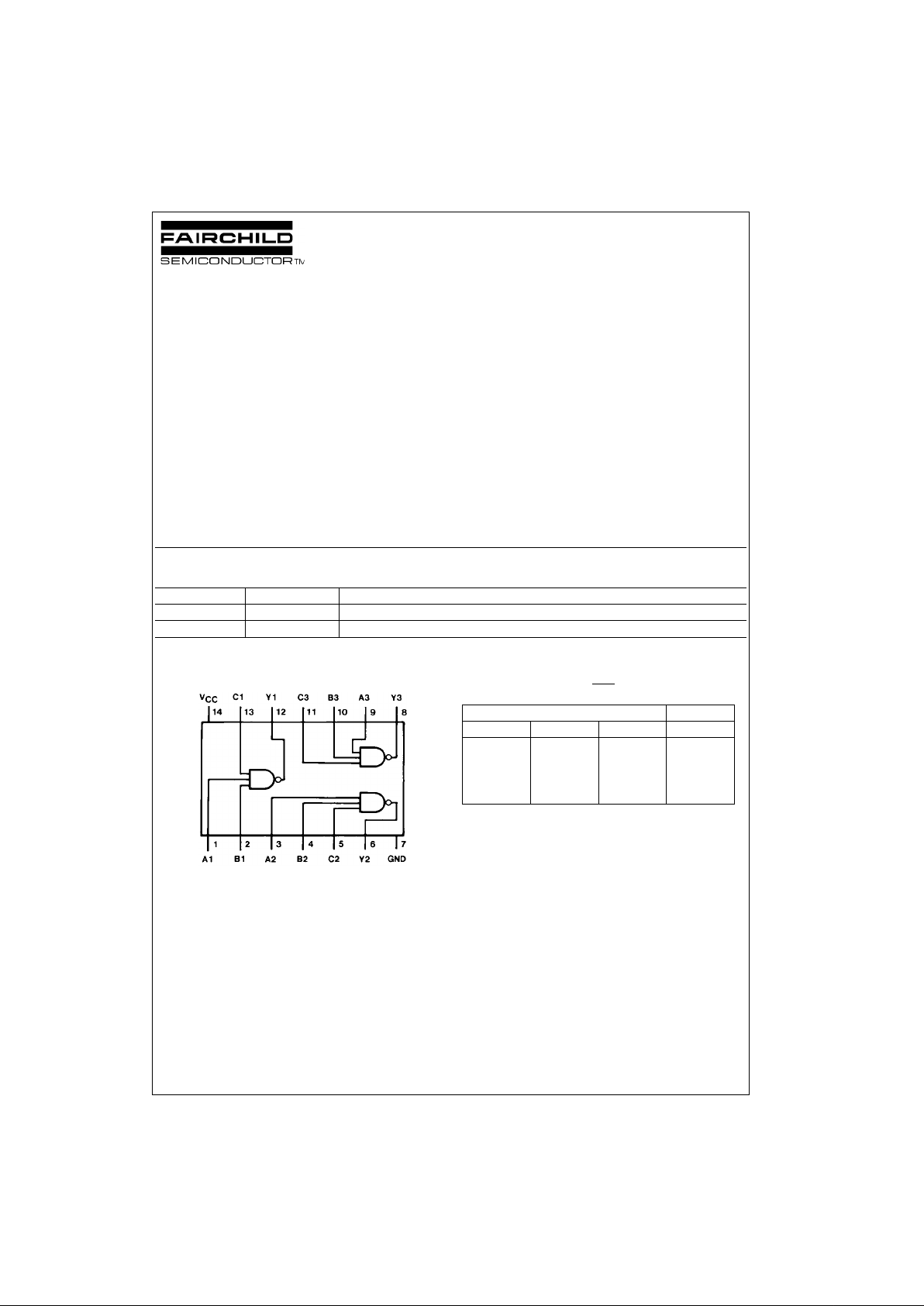
DM74AS10 Triple 3-Input NAND Gate
DM74AS10
Triple 3-Input NAND Gate
General Description
This device contains three independent gates, each of
which performs the logic NAND function.
Features
■ Switching specifications at 50 pF
■ Switching specifications guaranteed over full
temperat ure and V
CC
range
■ Advanced oxide-isolated, ion-implanted Schottky
TTL process
■ Functionally and pin for pin compatible with Schottky,
low power Schottky, and advanced low power Schottky
TTL counterpart
■ Improved AC performance over Schottky, low power
Schottky, and advanced low power Schottky counterparts
Ordering Code:
Devices also availab le in Tape and Reel. Specify by appending th e s uffix let t er “X” to the ordering code.
Connection Diagram Function Table
Y = ABC
H = HIGH Logic Level
L = LOW Logic Level
X = Either LOW or HIGH Logic Level
Order Number Package Number Package Description
DM74AS10M M14A 14-Lead Small Outline Integrated Circuit (SOIC), JEDEC MS-012, 0.150 Narrow
DM74AS10N N14A 14-Lead Plastic Dual-In-Line Package (PDIP), JEDEC MS-001, 0.300 Wide
Inputs Output
ABCY
XXLH
XLXH
LXXH
HHHL
www.fairchildsemi.com 2
DM74AS10
Absolute Maximum Ratings(Note 1)
Note 1: Note: The “Absol ute Maxim um Rati ngs” are th ose valu es beyond
which the safety of the device cannot be guaranteed. The device should not
be operated at the se lim its. Th e para met ric valu es d efine d in t he El ect rical
Characteristics tables are not guaranteed at the absolute maximum ratings.
The “Recommend ed O peratin g Cond itions” t able w ill defin e the co ndition s
for actual device operation.
Recommended Operating Conditions
Electrical Characteristics
over recommended operating free air temperature range. All typical values are measured at VCC = 5V, TA = 25°C.
Switching Characteristics
over recommended operating free air temperature range
Supply Voltage 7V
Input Voltage 7V
Operating Free Air Temperature Range 0°C to +70°C
Storage Temperature Range −65°C to +150°C
Typical θ
JA
N Package 84.0°C/W
M Package 114.0°C/W
Symbol Parameter Min Nom Max Units
V
CC
Supply Voltage 4.5 5 5.5 V
V
IH
HIGH Level Input Voltage 2 V
V
IL
LOW Level Input Voltage 0.8 V
I
OH
HIGH Level Output Current −2mA
I
OL
LOW Level Output Current 20 mA
T
A
Free Air Operating Temperature 0 70 °C
Symbol Parameter Conditions Min Typ Max Units
V
IK
Input Clamp Voltage VCC = 4.5V, II = −18 mA −1.2 V
V
OH
HIGH Level IOH = −2 mA
VCC − 2V
Output Voltage VCC = 4.5V to 5.5V
V
OL
LOW Level VCC = 4.5V
0.35 0.5 V
Output Voltage IOL = 20 mA
I
I
Input Current @ Max Input Voltag e VCC = 5.5V, VIH = 7V 0.1 mA
I
IH
HIGH Level Input Current VCC = 5.5V, VIH = 2.7V 20 µA
I
IL
LOW Level Input Current VCC = 5.5V, VIL = 0.4V −0.5 mA
I
O
Output Drive Current VCC = 5.5V, VO = 2.25V −30 −112 mA
I
CC
Supply Current VCC = 5.5V Outputs HIGH 1.5 2.4 mA
Outputs LOW 8.1 13 mA
Symbol Parameter Conditions Min Max Units
t
PLH
Propagation Delay Time VCC = 4.5V to 5.5V
14.5ns
LOW-to-HIGH Level Output RL = 500Ω
t
PHL
Propagation Delay Time CL = 50 pF
14.5ns
HIGH-to-LOW Level Output
 Loading...